Table of Contents
Advertisement
Quick Links
Advertisement
Table of Contents

Related Manuals for Aaeon PICO-APL4


Summary of Contents for Aaeon PICO-APL4
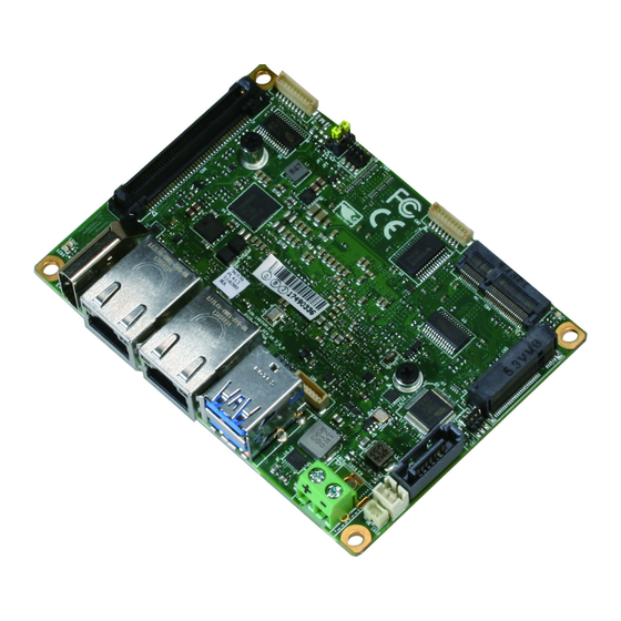
- Page 1 PICO-APL4 PICO-ITX Board User’s Manual 1 Last Updated: May 16, 2018...
- Page 2 AAEON assumes no liabilities resulting from errors or omissions in this document, or from the use of the information contained herein. AAEON reserves the right to make changes in the product design without notice to its users.
- Page 3 Acknowledgement All other products’ name or trademarks are properties of their respective owners. Microsoft Windows is a registered trademark of Microsoft Corp. ® ITE is a trademark of Integrated Technology Express, Inc. IBM, PC/AT, PS/2, and VGA are trademarks of International Business Machines ...
- Page 4 Packing List Before setting up your product, please make sure the following items have been shipped: Item Quantity PICO-APL4 Product DVD with drivers If any of these items are missing or damaged, please contact your distributor or sales representative immediately.
- Page 5 (if any), its specifications, dimensions, jumper/connector settings/definitions, and driver installation instructions (if any), to facilitate users in setting up their product. Users may refer to the AAEON.com for the latest version of this document. Preface...
- Page 6 Safety Precautions Please read the following safety instructions carefully. It is advised that you keep this manual for future references All cautions and warnings on the device should be noted. Make sure the power source matches the power rating of the device. Position the power cord so that people cannot step on it.
- Page 7 If any of the following situations arises, please the contact our service personnel: Damaged power cord or plug Liquid intrusion to the device iii. Exposure to moisture Device is not working as expected or in a manner as described in this manual The device is dropped or damaged Any obvious signs of damage displayed on the device...
- Page 8 FCC Statement This device complies with Part 15 FCC Rules. Operation is subject to the following two conditions: (1) this device may not cause harmful interference, and (2) this device must accept any interference received including interference that may cause undesired operation.
- Page 9 China RoHS Requirements (CN) 产品中有毒有害物质或元素名称及含量 AAEON Main Board/ Daughter Board/ Backplane 有毒有害物质或元素 部件名称 铅 汞 镉 六价铬 多溴联苯 多溴二苯醚 (Pb) (Hg) (Cd) (Cr(VI)) (PBB) (PBDE) 印刷电路板 ○ ○ ○ ○ ○ ○ 及其电子组件 外部信号 ○ ○ ○ ○ ○ ○...
- Page 10 China RoHS Requirement (EN) Poisonous or Hazardous Substances or Elements in Products AAEON Main Board/ Daughter Board/ Backplane Poisonous or Hazardous Substances or Elements Hexavalent Polybrominated Polybrominated Component Lead Mercury Cadmium Chromium Biphenyls Diphenyl Ethers (Pb) (Hg) (Cd) (Cr(VI)) (PBB) (PBDE) PCB &...
-
Page 11: Table Of Contents
Table of Contents Chapter 1 - Product Specifications..................1 Specifications ......................2 Chapter 2 – Hardware Information ..................4 Dimensions ....................... 5 Jumpers and Connectors ..................8 List of Jumpers ......................10 2.3.1 Auto Power Button Enable/Disable Selection (JP1) ......11 2.3.2 Clear CMOS Jumper (JP2) .............. - Page 12 LPC Port (CN22) ..................38 Electrical Specifications for I/O Ports ..............40 Function Block ......................41 Assembly Options ....................42 2.7.1 PICO-APL4-HSK01 ..................42 2.7.2 PICO-APL4-HSP01................... 43 Chapter 3 - AMI BIOS Setup ....................44 System Test and Initialization ................45 AMI BIOS Setup .....................
- Page 13 Setup submenu: Exit ..................... 65 Chapter 4 – Drivers Installation .................... 66 Product CD/DVD ....................67 Appendix A - Watchdog Timer Programming ..............69 Watchdog Timer Registers .................. 70 Watchdog Sample Program ................. 71 Appendix B - I/O Information ....................74 I/O Address Map ....................
-
Page 14: Chapter 1 - Product Specifications
Chapter 1 Chapter 1 - Product Specifications... -
Page 15: Specifications
Specifications System PICO-ITX Form Factor Intel® Atom™ Processor SoC Up to 2.4GHz CPU Frequency Intel® Atom™ Processor SoC Chipset Onboard DDR3L 2G (Optional to 4G) Memory Type Up to 4GB Max. Memory Capacity AMI / SPI BIOS ... - Page 16 Certification CE, FCC Display Chipset Intel® Atom™ Processor SoC HDMI 1.4b: 3840 x 2160@30Hz) Resolution Internal eDP: 3840x2160@60Hz (Optional) DDI (Optional from BIO) LCD Interface SATA 6.0Gb/s x 1, 5V Power reserved Storage M.2 2280 (B Key) x 1 eMMC 16G (optional to 32/64G) Realtek 8111G x 2 Ethernet...
-
Page 17: Chapter 2 - Hardware Information
Chapter 2 Chapter 2 – Hardware Information... -
Page 18: Dimensions
Dimensions Component Side Component Side Chapter 2 – Hardware Information... - Page 19 Solder Side Solder Side Chapter 2 – Hardware Information...
- Page 20 Rear I/O Configuration Phoenix DC Jack Chapter 2 – Hardware Information...
-
Page 21: Jumpers And Connectors
Jumpers and Connectors Component Side Component Side Chapter 2 – Hardware Information... - Page 22 Solder Side Solder Side Chapter 2 – Hardware Information...
-
Page 23: List Of Jumpers
List of Jumpers Please refer to the table below for all of the board’s jumpers that you can configure for your application Label Function Auto Power Button Enable/Disable Selection Clear CMOS Jumper Chapter 2 – Hardware Information... -
Page 24: Auto Power Button Enable/Disable Selection (Jp1)
2.3.1 Auto Power Button Enable/Disable Selection (JP1) 1 2 3 Enable/AT (Default) Disable/ATX ※ When disabled, the power button of CN3 (1-2) will be used to power on the system 2.3.2 Clear CMOS Jumper (JP2) Normal (Default) Clear CMOS Chapter 2 – Hardware Information... -
Page 25: List Of Connectors
List of Connectors Please refer to the table below for all of the board’s connectors that you can configure for your application Label Function COM Port 2 COM Port 1 Front Panel Connector M.2 Key-E Slot (2230) M.2 Key-B Slot (2280) BIO Port (Optional) Digital I/O SATA Port... -
Page 26: Com Port 2 (Cn1)
2.4.1 COM Port 2 (CN1) RS232 Pin Name Signal Type Pin Name DCD2 DSR2 RTS2 ±5V ±5V CTS2 DTR2 ±5V RI2/+5V/+12V +5V/+12V Chapter 2 – Hardware Information... - Page 27 RS485 Pin Name Signal Type Pin Name RS485_ D2- ±5V RS485_D2+ ±5V NC/+5V/+12V +5V/+12V RS422 Pin Name Signal Type Pin Name RS422_TX2- ±5V RS422_TX2+ ±5V RS422_RX2+ RS422_RX2- NC/+5V/+12V +5V/+12V ※ COM2 RS-232/422/485 can be set by BIOS setting. Default is RS-232. ※...
-
Page 28: Com Port 1 (Cn2)
2.4.2 COM Port 1 (CN2) RS232 Pin Name Signal Type Pin Name DCD1 DSR1 RTS1 ±9V ±9V CTS1 DTR1 ±9V Chapter 2 – Hardware Information... -
Page 29: Front Panel Connector (Cn3)
2.4.3 Front Panel Connector (CN3) Pin Name Pin Name PWR_BTN- PWR_BTN+ HDD_LED- HDD_LED+ SPEAKER- SPEAKER+ PWR_LED- PWR_LED+ H/W RESET- H/W RESET+ 2.4.4 M.2 Key-E Slot (2230) (CN4) Pin Name Signal Type Signal Level +3.3VSB +3.3V USB_D+ DIFF +3.3V +3.3VSB USB_D- DIFF Chapter 2 –... - Page 30 PCIE_TX+ DIFF Chapter 2 – Hardware Information...
- Page 31 PCIE_TX- DIFF PCIE_RX+ DIFF PCIE_RX- DIFF PCIE_REF_CLK+ DIFF PCIE_REF_CLK- DIFF PCIE_RST# +3.3V PCIE_CLK_REQ# +3.3V W_DISABLE2# +3.3V PCIE_WAKE# +3.3V W_DISABLE1# +3.3V Chapter 2 – Hardware Information...
- Page 32 +3.3VSB +3.3V +3.3VSB +3.3V +3.3VSB +3.3V Chapter 2 – Hardware Information...
-
Page 33: Key-B Slot (2280) (Cn5)
2.4.5 M.2 Key-B Slot (2280) (CN5) Pin Name Signal Type Signal Level +3.3V +3.3V +3.3V +3.3V USB_D+ DIFF USB_D- DIFF +3.3V SSD_DAS# Chapter 2 – Hardware Information... - Page 34 DEVSLP +1.8V SATA_RX+ DIFF SATA_RX- DIFF SATA_TX- DIFF Chapter 2 – Hardware Information...
- Page 35 SATA_TX+ DIFF Chapter 2 – Hardware Information...
-
Page 36: Bio Port (Optional) (Cn6)
+3.3V +3.3V +3.3V +3.3V +3.3V +3.3V 2.4.6 BIO Port (Optional) (CN6) Pin Name Signal Type Signal Level +12VSB +12V PCIE_TXN0 DIFF PCIE_RXN0 DIFF PCIE_TXP0 DIFF PCIE_RXP0 DIFF Chapter 2 – Hardware Information... - Page 37 Pin Name Signal Type Signal Level PCIE_TXN1 DIFF PCIE_RXN1 DIFF PCIE_TXP1 DIFF PCIE_RXP1 DIFF PS_ON# DDI_DDCCLK +3.3V DDI_DDCDATA +3.3V +5VSB +5VSB +5VSB +5VSB PCIE_REF_CLK0 DIFF RESET# PCIE_REF_CLK0# DIFF DDI_TX1N DIFF DDI_TX0N DIFF DDI_TX1P DIFF DDI_TX0P DIFF Chapter 2 – Hardware Information...
- Page 38 Pin Name Signal Type Signal Level DDI_TX3N DIFF DDI_TX2N DIFF DDI_TX3P DIFF DDI_TX2P DIFF DDI_HPD DDI_AUXN DIFF DDI0_AUXP DIFF USB3_TX_N DIFF USB_D0- DIFF USB3_TX_P DIFF USB_D0+ DIFF USB3_RX_N DIFF USB3_RX_P DIFF SMB_CLK +3.3V SMB_DATA +3.3V Chapter 2 – Hardware Information...
- Page 39 Pin Name Signal Type Signal Level WAKE# +3.3V USB_OC# +3.3V USB_OC# +3.3V LPC_AD0 +3.3V LPC_FRAME# +3.3V LPC_AD1 +3.3V SERIRQ +3.3V LPC_AD2 +3.3V LPC_AD3 +3.3V BIO_PWOK +3.3V AGND LPC_CLK +3.3V PME# +3.3V Chapter 2 – Hardware Information...
-
Page 40: Digital I/O (Cn7)
2.4.7 Digital I/O (CN7) Pin Name Signal Type Signal Level DIO0 DIO1 DIO2 DIO3 Chapter 2 – Hardware Information... -
Page 41: Sata Port (Cn8)
2.4.8 SATA Port (CN8) Pin 1 Pin 7 Pin Name Signal Type Signal Level SATA_TX+ DIFF SATA_TX- DIFF SATA_RX- DIFF SATA_RX+ DIFF Chapter 2 – Hardware Information... -
Page 42: Spi Flash Programming Port (Cn9)
2.4.9 SPI Flash Programming Port (CN9) Pin Name Signal Type Signal Level SPI_MISO SPI_CLK +3.3VSB +3.3V SPI_MOSI SPI_CS Chapter 2 – Hardware Information... -
Page 43: Output For Sata Hdd (Cn12)
2.4.10 +5V Output for SATA HDD (CN12) Pin Name Signal Type Signal Level 2.4.11 HDMI Port (CN11) Pin Name Signal Type Signal level TMDS_DAT2+ DIFF TMDS_DAT2- DIFF TMDS_DAT1+ DIFF TMDS_DAT1- DIFF TMDS_DAT0+ DIFF TMDS_DAT0- DIFF Chapter 2 – Hardware Information... -
Page 44: Battery (Cn12)
Pin Name Signal Type Signal level TMDS_CLK+ DIFF TMDS_CLK- DIFF DDC_CLK DDC_DATA HPLG_DETECT 2.4.12 Battery (CN12) Pin Name Signal Type Signal Level 3.3V +3.3V Chapter 2 – Hardware Information... -
Page 45: Lan (Rj-45) Port1 (Cn13)
2.4.13 LAN (RJ-45) Port1 (CN13) Pin Name Signal Type Signal level DIFF MDI0+ DIFF MDI0- DIFF MDI1+ DIFF MDI2+ DIFF MDI2- DIFF MDI1- DIFF MDI3+ DIFF MDI3- Chapter 2 – Hardware Information... -
Page 46: Lan (Rj-45) Port2 (Cn14)
2.4.14 LAN (RJ-45) Port2 (CN14) Pin Name Signal Type Signal Level DIFF MDI0+ DIFF MDI0- DIFF MDI1+ DIFF MDI2+ DIFF MDI2- DIFF MDI1- DIFF MDI3+ DIFF MDI3- Chapter 2 – Hardware Information... -
Page 47: Usb 3.0 Ports 0 And 1 (Cn15)
2.4.15 USB 3.0 Ports 0 and 1 (CN15) Pin Name Signal Type Signal Level +5VSB DIFF USB0_D- DIFF USB0_D+ USB0_SSRX− DIFF USB0_SSRX+ DIFF USB0_SSTX− DIFF USB0_SSTX+ DIFF +5VSB DIFF USB1_D- DIFF USB1_D+ USB1_SSRX− DIFF Chapter 2 – Hardware Information... -
Page 48: External Power Input (Cn17)
Pin Name Signal Type Signal Level USB1_SSRX+ DIFF USB1_SSTX− DIFF USB1_SSTX+ DIFF 2.4.16 External Power Input (CN17) Pin Name Signal Type Signal Level +VIN +12V 2.4.17 +12V DC Power Jack (Optional) (CN18) Pin Name Signal Type Signal Level +12V +12V Chapter 2 –... -
Page 49: Embedded Displayport (Optional) (Cn19)
2.4.18 Embedded DisplayPort (Optional) (CN19) Pin Name Signal Type Signal Level +12V +12V +12V +12V EDP_TX2_N DIFF EDP_TX2_P DIFF EDP_TX1_N DIFF EDP_TX1_P DIFF EDP_TX0_N DIFF EDP_TX0_P DIFF EDP_TX3_N DIFF EDP_TX3_P DIFF EDP_AUXN DIFF EDP_AUXP DIFF Chapter 2 – Hardware Information... -
Page 50: Usb 2.0 Port 2 (Cn20)
EDP_BKLTNESS +3.3V EDP_BKLTEN +3.3V EDP_HPD +12V +12V +12V +12V +12V +12V +12V +12V 2.4.19 USB 2.0 Port 2 (CN20) Pin Name Signal Type Signal Level +5VSB USB_D- DIFF USB_D+ DIFF Chapter 2 – Hardware Information... -
Page 51: Usb 2.0 Port 1 (Cn21)
2.4.20 USB 2.0 Port 1 (CN21) Pin Name Signal Type Signal Level +5VSB USB_D- DIFF USB_D+ DIFF 2.4.21 LPC Port (CN22) Pin Name Signal Type Signal Level +3.3V LAD0 +3.3V LAD1 +3.3V LAD2 Chapter 2 – Hardware Information... - Page 52 +3.3V LAD3 +3.3V +3.3V LFRAME# +3.3V LRESET# LCLK +3.3V I2C0_SDA +3.3V I2C0_SCL +3.3V SERIRQ Chapter 2 – Hardware Information...
-
Page 53: Electrical Specifications For I/O Ports
Electrical Specifications for I/O Ports Reference Signal Name Rate Output COM Port 2 +5V/+12V +5V/0.5A or +12V/0.5A M.2 Key-E Slot (2230) +3.3VSB +3.3V/2A M.2 Key-B Slot (2280) +3.3V +3.3V/2.5A Digital IO Port +5V/1A +5V Output for SATA HDD CN10 +5V/1A USB Ports 0 and 1 CN15 +5VSB... -
Page 54: Function Block
Function Block Chapter 2 – Hardware Information... -
Page 55: Assembly Options
Assembly Options 2.7.1 PICO-APL4-HSK01 Chapter 2 – Hardware Information... -
Page 56: Pico-Apl4-Hsp01
2.7.2 PICO-APL4-HSP01 Chapter 2 – Hardware Information... -
Page 57: Chapter 3 - Ami Bios Setup
Chapter 3 Chapter 3 - AMI BIOS Setup... -
Page 58: System Test And Initialization
4. The CMOS memory has lost power and the configuration information has been erased. The PICO-APL4 CMOS memory has an integral lithium battery backup for data retention. However, you will need to replace the complete unit when it finally runs down. -
Page 59: Ami Bios Setup
AMI BIOS Setup AMI BIOS ROM has a built-in Setup program that allows users to modify the basic system configuration. This type of information is stored in battery-backed CMOS RAM and BIOS NVRAM so that it retains the Setup information when the power is turned off. Entering Setup Power on the computer and press <Del>or <ESC>... -
Page 60: Setup Submenu: Main
Setup Submenu: Main Chapter 3 – AMI BIOS Setup... -
Page 61: Setup Submenu: Advanced
Setup Submenu: Advanced Chapter 3 – AMI BIOS Setup... -
Page 62: Trusted Computing
3.4.1 Trusted Computing Options summary: Security Device Disable Support Enable Optimal Default, Failsafe Default Enables or Disables BIOS support for security device. O.S. will not show Security Device. TCG EFI protocol and INT1A interface will not be available. SHA-1 PCR Bank Disable Enable Optimal Default, Failsafe Default... - Page 63 Platform Hierarchy Disabled Enabled Optimal Default, Failsafe Default Enable or disable Platform Hierarchy Storage Hierarchy Disabled Enabled Optimal Default, Failsafe Default Enable or Disable Storage Hierarchy Endorsement Disabled Hierarchy Enabled Optimal Default, Failsafe Default Enable or Disable Endorsement Hierarchy TPM2.0 UEFI Spec TCG_1_2 Version TCG_2...
-
Page 64: Cpu Configuration
3.4.2 CPU Configuration Options summary: C-States Disabled Enabled Optimal Default, Failsafe Default Enable/Disable C States. EIST™ Disabled Enabled Optimal Default, Failsafe Default Enable/Disable Intel SpeedStep. Turbo Mode Disabled Enabled Optimal Default, Failsafe Default Turbo Mode Intel Virtualization Disabled Technology Enabled Optimal Default, Failsafe Default When enabled, a VMM can utilize the additional hardware capabilities provided by Vanderpool Technology. - Page 65 Power Limit 1 Enable Disabled Optimal Default, Failsafe Default Enabled Enable/Disable Power Limit 1 Chapter 3 – AMI BIOS Setup...
-
Page 66: Sata Configuration
3.4.3 SATA Configuration Options summary: Chipset SATA Disabled Enabled Optimal Default, Failsafe Default Enables or Disables the Chipset SATA Controller. The Chipset SATA controller supports the 2 black internal SATA ports (up to 3Gb/s supported per port). Port 0 Disabled Enabled Optimal Default, Failsafe Default Enable or Disable SATA Port... -
Page 67: Hardware Monitor
3.4.4 Hardware Monitor Chapter 3 – AMI BIOS Setup... -
Page 68: Sio Configuration
3.4.5 SIO Configuration Chapter 3 – AMI BIOS Setup... -
Page 69: Serial Port 1 Configuration
3.4.5.1 Serial Port 1 Configuration Options summary: Use This Device Disable Enable Optimal Default, Failsafe Default Enable or Disable this Logical Device. Possible: Use Automatic Settings Optimal Default, Failsafe Default IO=3F8h; IRQ=4 IO=2F8h; IRQ=3 Allows user to change Device's Resource settings. New settings will be reflected on This Setup Page after System restarts. -
Page 70: Serial Port 1 Configuration
3.4.5.1 Serial Port 1 Configuration Options summary: Use This Device Disable Enable Optimal Default, Failsafe Default Enable or Disable this Logical Device. Possible: Use Automatic Settings Optimal Default, Failsafe Default IO=2F8h; IRQ=3 IO=3F8h; IRQ=4 Allows user to change Device's Resource settings. New settings will be reflected on This Setup Page after System restarts. -
Page 71: Digital Io Port Configuration
3.4.5 Digital IO Port Configuration Options summary: DIO Port* Output Input Set DIO as Input or Output Output Level High Optimal Default, Failsafe Default Set output level when DIO pin is output Chapter 3 – AMI BIOS Setup... -
Page 72: Power Management
3.4.6 Power Management Options summary: Power Mode ATX Type Optimal Default, Failsafe Default AT Type Select system power mode Restore AC Power Last State Optimal Default, Failsafe Default Loss Always On Always Off RTC wake system Disable Optimal Default, Failsafe Default from S5 Fixed Time Fixed Time: System will wake on the hr::min::sec specified. -
Page 73: Setup Submenu: Chipset
Setup submenu: Chipset Chapter 3 – AMI BIOS Setup... -
Page 74: North Bridge
3.5.1 North Bridge Chapter 3 – AMI BIOS Setup... -
Page 75: South Bridge
3.5.2 South Bridge Options summary: M.2 PCI Express Disable Root Port Enable Optimal Default, Failsafe Default Auto Control the PCI Express Root Port. AUTO: To disable unused root port automatically for the most optimum power savings. Enable: Enable PCIe root port Disable: Disable PCIe root port M.2 PCIe Speed Auto... -
Page 76: Setup Submenu: Security
Setup submenu: Security Change User/Supervisor Password You can install a Supervisor password, and if you install a supervisor password, you can then install a user password. A user password does not provide access to many of the features in the Setup utility. If you highlight these items and press Enter, a dialog box appears which lets you enter a password. -
Page 77: Setup Submenu: Boot
Setup submenu: Boot Options summary: Quiet Boot Disabled Enabled Optimal Default, Failsafe Default EnableDisable showing boot logo. Monitor Mwait Disable Enabled Auto Optimal Default, Failsafe Default Enable/Disable Monitor Mwait. To install Linux OS, please set this item to disable. Ipv4 PXE Support Disabled Optimal Default, Failsafe Default Enabled... -
Page 78: Setup Submenu: Exit
Setup submenu: Exit Chapter 3 – AMI BIOS Setup... -
Page 79: Chapter 4 - Drivers Installation
Chapter 4 Chapter 4 – Drivers Installation... -
Page 80: Product Cd/Dvd
Product CD/DVD The PICO-APL4 comes with a product DVD that contains all the drivers and utilities you need to setup your product. Insert the DVD and follow the steps in the autorun program to install the drivers. In case the program does not start, follow the sequence below to install the drivers. - Page 81 Step 4 – Install Audio Driver Open the STEP4 - AUDIO folder and open the 0006-64bit_Win7_Win8_Win81_Win10_R279.exe file Follow the instructions Driver will be installed automatically Step 5 – Install TXE Driver Open the STEP5 - TXE folder and open the SetupTXE.exe file Follow the instructions Driver will be installed automatically Step 6 –...
-
Page 82: Appendix A - Watchdog Timer Programming
Appendix A Appendix A - Watchdog Timer Programming... -
Page 83: Watchdog Timer Registers
Watchdog Timer Registers Table 1 : Watch dog relative IO address Default Value Note I/O Base I/O Base address for Watchdog operation. 0x2E Address This address is assigned by SIO LDN7 Table 2 : Watchdog relative register table Register Offset BitNum Value Note... -
Page 84: Watchdog Sample Program
A.2 Watchdog Sample Program ****************************************************************************** // WDT I/O operation relative definition (Please reference to Table 1) #define WDTAddr 0x510 // WDT I/O base address Void WDTWriteByte(byte Register, byte Value); byte WDTReadByte(byte Register); Void WDTSetReg(byte Register, byte Bit, byte Val); // Watch Dog relative definition (Please reference to Table 2) #define DevReg 0x00 // Device configuration register #define WDTRstBit 0x80 // Watchdog WDTRST# (Bit7) - Page 85 ******************************************************************************* // Procedure : AaeonWDTEnable VOID EnterSIOconfig IOWriteByte (IoConfAddr,0x87); IOWriteByte (IoConfAddr,0x87); VOID ExitSIOconfig IOWriteByte (IoConfAddr,0xAA); VOID SetWDT IOWriteByte (IoConfAddr,0x2B); IOWriteByte(IoConfAddr+1, (IOReadByte(IoConfAddr+1)&0xFC)); // Procedure : AaeonWDTEnable AaeonWDTEnable () VOID WDTEnableDisable(1); // Procedure : AaeonWDTConfig AaeonWDTConfig (byte Counter, BOOLEAN Unit) VOID // Disable WDT counting WDTEnableDisable( // Clear Watchdog Timeout Status WDTClearTimeoutStatus();...
- Page 86 WDTSetBit( TimerReg, UnitBit, Unit // WDT output mode set to pulse WDTSetBit( TimerReg, ModeBit, ModeVal // WDT output mode set to active low WDTSetBit( TimerReg, PolarityBit, PolarityVal // WDT output pulse width is 25ms WDTSetBit( TimerReg, PSWidthBit, PSWidthVal // Watchdog WDTRST# Enable WDTSetBit( DevReg, WDTRstBit, WDTRstVal WDTClearTimeoutStatus()
-
Page 87: Appendix B - I/O Information
Appendix B Appendix B - I/O Information... -
Page 88: I/O Address Map
I/O Address Map Appendix B – I/O Information... -
Page 89: Memory Address Map
Memory Address Map Appendix B – I/O Information... -
Page 90: Irq Mapping Chart
IRQ Mapping Chart Appendix B – I/O Information... - Page 91 Appendix B – I/O Information...
- Page 92 Appendix B – I/O Information...
-
Page 93: Appendix C - Mating Connectors
Appendix C Appendix C – Mating Connectors... -
Page 94: List Of Mating Connectors And Cables
List of Mating Connectors and Cables The table notes mating connectors and available cables. Connector Function Mating Connector Available Cable P/N Label Cable Vendor Model no COM Port #2 Serial Port SHR-09V-S-B 1701090122 Connector Cable COM Port #1 Serial Port SHR-09V-S-B 1701090122 Connector... - Page 95 Connector AAEON LPC CN22 SHR-12V-S-B 1703120130 Connector Cable Appendix C – Mating Connectors...
-
Page 96: Appendix D - Dio
Appendix D Appendix D –... -
Page 97: Dio
The PICO-APL4 provides one serial access interface, I2C Bus, to read/write internal registers. The address of Serial Bus is 0x6E (0110_1110) The related register for configuring DIO is list as follows: Configuration and Control Register – Index 01h Power-on default [7:0] =0000_1000b... - Page 98 The following is a sample code for 8 input .MODEL SMALL .CODE begin: mov cl,01h mov al,80h call CT_I2CWriteByte call Delay5ms mov al,00h mov cl,20h call CT_I2CWriteByte mov cl,22h call CT_I2CReadByte ;Input : CL - register index Appendix D –DIO...
- Page 99 ; CH - device ID ;Output : AL - Value read Ct_I2CReadByte Proc Near mov ch,06eh mov dx, F040h + 00h ; Host Control Register xor al, al ; Clear previous commands out dx, al call Delay5ms mov dx, F040h + 04h ; Transmit Slave Address Register inc ch ;...
- Page 100 in al, dx Ct_I2CReadByte Endp ;Input : CL - register index ; CH - device ID ; AL - Value to write ;Output: none Ct_I2CWriteByte Proc Near mov ch,06eh xchg ah, al mov dx, F040h + 00h ; Host Control Register xor al, al ;...
- Page 101 out dx, al mov dx, F040h + 00h ; Host Control Register mov al, 12h ; Start a byte access out dx, al call CT_Chk_SMBus_Ready ;R14 Ct_I2CWriteByte Endp ; Wait until the busy bit clears, indicating that the SMBUS ; activity has concluded. CT_Chk_SMBus_Ready Proc Near mov dx, F040h + 01h ;...
Need help?
Do you have a question about the PICO-APL4 and is the answer not in the manual?
Questions and answers