
Related Manuals for National Instruments AT-DIO-32F


Summary of Contents for National Instruments AT-DIO-32F
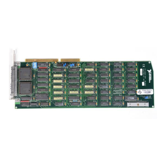
- Page 1 AT-DIO-32F User Manual High-Speed 32-Bit Parallel Digital I/O Interface for the PC April 1995 Edition Part Number 320147-01 © Copyright 1989, 1995 National Instruments Corporation. All Rights Reserved.
- Page 2 National Instruments Corporate Headquarters 6504 Bridge Point Parkway Austin, TX 78730-5039 (512) 794-0100 Technical support fax: (800) 328-2203 (512) 794-5678 Branch Offices: Australia (03) 879 9422, Austria (0662) 435986, Belgium 02/757.00.20, Canada (Ontario) (519) 622-9310, Canada (Québec) (514) 694-8521, Denmark 45 76 26 00, Finland (90) 527 2321, France (1) 48 14 24 24,...
- Page 3 Limited Warranty The AT-DIO-32F is warranted against defects in materials and workmanship for a period of one year from the date of shipment, as evidenced by receipts or other documentation. National Instruments will, at its option, repair or replace equipment that proves to be defective during the warranty period. This warranty includes parts and labor.
- Page 4 Any use or application of National Instruments products for or involving medical or clinical treatment must be performed by properly trained and qualified medical personnel, and all traditional medical safeguards, equipment, and procedures that are appropriate in the particular situation to prevent serious injury or death should always continue to be used when National Instruments products are being used.
-
Page 5: Table Of Contents
I/O Connector Electrical Specifications ................ 2-16 I/O Signals Rating ..................... 2-16 Input Signal Specifications................2-16 Output Signal Specifications ................2-16 Timing Specifications....................2-16 AT-DIO-32F Read and Write Timing ............... 2-18 Cabling .......................... 2-19 Chapter 3 Theory of Operation ......................3-1 Address Decoder ...................... - Page 6 CNTR2 Register (REQ2 Generator) ............. 4-31 CNTR3 Register (Timebase Generator) ..........4-32 CNTRCMD Register ................4-33 Programming Considerations ..................4-37 Initializing the AT-DIO-32F Board ..............4-37 Mode 0 Programming..................4-38 Mode 1 Programming..................4-38 Leading Edge Mode ................4-41 Trailing Edge Mode................4-42 Data Settling Delay ................
- Page 7 Cabling ......................C-1 Sending Files to be Printed................C-2 AT-DIO-32F to AT-DIO-32F 16-Bit Communications..........C-4 Cabling ......................C-5 Sending and Receiving files with the AT-DIO-32F.......... C-5 The AT-DIO-32F and I/O Module Racks ..............C-10 Appendix D Intel Data Sheet ........................D-1 ©...
- Page 8 Drive RTSI Bus Clock Signal with Onboard Oscillator ........2-11 Figure 2-12. Digital I/O Connector Pin Assignments ............2-13 Figure 3-1. AT-DIO-32F Block Diagram ................3-1 Figure 3-2. AT-DIO-32F Clock Routing Scheme..............3-4 Figure 3-3. Level Mode – Read ................... 3-5 Figure 3-4.
- Page 9 Tables Table 2-1. AT-DIO-32F Factory-Set Jumper and Switch Settings ........2-2 Table 2-2. Default Settings of National Instruments Products for the PC......2-6 Table 2-3. Switch Settings with Corresponding Base I/O Address and Base I/O Address Space ..................2-7 Table 2-4.
-
Page 10: About This Manual
The AT-DIO-32F is a high-speed, 32-bit, parallel, digital I/O interface. The AT-DIO-32F is a member of the National Instruments AT Series of PC AT I/O channel expansion boards for the IBM PC AT and compatible computers. These boards are designed for high-performance data acquisition and control for applications in laboratory testing, production testing, and industrial process monitoring and control. -
Page 11: Conventions Used In This Manual
Intel 8254 System Timing Controller technical manual Customer Communication National Instruments wants to receive your comments on our products and manuals. We are interested in the applications you develop with our products, and we want to help if you have problems with them. -
Page 12: Chapter 1 Introduction
This chapter describes the AT-DIO-32F, lists the contents of your AT-DIO-32F kit, and explains how to unpack the AT-DIO-32F kit. The AT-DIO-32F is a high-speed, 32-bit, parallel, digital I/O interface board for the PC. The 32 lines of digital I/O are organized into four 8-bit ports. With the various handshaking options available, the AT-DIO-32F is compatible with a wide range of peripheral devices and other computers. -
Page 13: What Your Kit Should Contain
Introduction Chapter 1 What Your Kit Should Contain The contents of the AT-DIO-32F kit (part number 776246-01) are listed as follows. Kit Component Part Number AT-DIO-32F board 180735-01 AT-DIO-32F User Manual 320147-01 NI-DAQ software for DOS/Windows/LabWindows, with manuals 776250-01 NI-DAQ Software Reference Manual for DOS/Windows/LabWindows... -
Page 14: Optional Software
Normally, however, you should not need to read the low-level programming details in the user manual because the NI-DAQ software package for controlling the AT-DIO-32F is included with the board. Using NI-DAQ is quicker and easier than and as flexible as using the low-level programming described in Chapter 4, Programming. -
Page 15: Optional Equipment
1.0 m 180723-10 * The AT-DIO-32F is equipped with an EMI shield on the I/O connector that can be used to connect the shield of a shielded ribbon cable to the computer chassis. Shielded ribbon cables are necessary to meet FCC Class A Emission Limits. -
Page 16: Unpacking
• Remove the board from the package and inspect the board for loose components or any other sign of damage. Notify National Instruments if the board appears damaged in any way. Do not install a damaged board into your computer. -
Page 17: Configuration And Installation
AT Bus Interface The AT-DIO-32F is configured at the factory to use a base I/O address of hex 240, to use interrupt lines 11 and 12, to use DMA channels 5 and 6, and to disconnect the board from the RTSI clock. -
Page 18: Table 2-1. At-Dio-32F Factory-Set Jumper And Switch Settings
Configuration and Installation Chapter 2 Table 2-1. AT-DIO-32F Factory-Set Jumper and Switch Settings Base I/O Address Hex 240 (factory setting) The black side indicates the side that is pushed down. DMA Channel Bank A = Channel 5 W1: Upper-right two rows... -
Page 20: Base I/O Address Selection
If any equipment in your computer uses this base I/O address space, change the base I/O address of the AT-DIO-32F or of the other device. If you change the AT- DIO-32F base I/O address, make a corresponding change to any software packages you use with the AT-DIO-32F. -
Page 21: Figure 2-2. Example Base I/O Address Switch Settings
B. Switches Set to Base I/O Address of Hex 240 (Factory Setting) Figure 2-2. Example Base I/O Address Switch Settings The five LSBs of the address (A4 through A0) are decoded by the AT-DIO-32F to select the appropriate AT-DIO-32F register. To change the base I/O address, remove the plastic cover on U61, press each switch to the desired position, verify that each switch is completely pressed down, and replace the plastic cover. -
Page 22: Table 2-2. Default Settings Of National Instruments Products For The Pc
Configuration and Installation Chapter 2 Table 2-2. Default Settings of National Instruments Products for the PC Board DMA Channel Interrupt Level Base I/O Address AT-A2150 None* None* 120 hex AT-AO-6/10 Channel 5 Lines 11, 12 1C0 hex AT-DIO-32F Channels 5, 6... -
Page 23: Dma Channel Selection
The DMA channel used by the AT-DIO-32F is selected by jumpers on W1 (see Figure 2-1). The AT-DIO-32F is set at the factory to use DMA Channels 5 and 6. These are the default DMA channels used by the AT-DIO-32F software handler. Verify that these DMA channels are not also used by equipment already installed in your computer. -
Page 24: Figure 2-3. Dma Jumper Settings For Dma Channels 5 And 6 (Factory Settings)
Configuration and Installation Chapter 2 The AT-DIO-32F hardware can only use Channels 5, 6, and 7 as DMA channels. Notice that these are the three available 16-bit channels on the PC I/O channel. The AT-DIO-32F does not use and cannot be configured to use the 8-bit DMA channels on the PC I/O channel. -
Page 25: Interrupt Selection
Figure 2-5. DMA Jumper Settings for Disabling DMA Transfers Interrupt Selection The AT-DIO-32F board can connect to one or two of any of the 11 interrupt lines of the PC I/O channel. The interrupt lines are selected by jumper W2, which is located above the I/O slot edge connector on the AT-DIO-32F (see Figure 2-1). -
Page 26: Rtsi Bus Clock Selection
Chapter 2 If you do not want to use interrupts, place the jumper on W2 in the positions shown in Figure 2- 7. This setting disables the AT-DIO-32F from asserting any interrupt lines on the PC I/O channel. • • • • • • • • •... -
Page 27: Figure 2-9. Disconnect From Rtsi Bus Clock; Use Onboard Oscillator (Factory Settings)
Figure 2-9. Disconnect from RTSI Bus Clock; Use Onboard Oscillator (Factory Settings) STANDBY • • BRDCLK BRDCLK RTSICLK Figure 2-10. Receive RTSI Bus Clock Signal • • STANDBY BRDCLK BRDCLK RTSICLK Figure 2-11. Drive RTSI Bus Clock Signal with Onboard Oscillator © National Instruments Corporation 2-11 AT-DIO-32F User Manual... -
Page 28: Installation
2. Remove the top cover or access port to the I/O channel. 3. Remove the expansion slot cover on the back panel of the computer. 4. Insert the AT-DIO-32F into a 16-bit slot. It may be a tight fit, but do not force the board into place. -
Page 29: Signal Connections
Warning: Connections that exceed any of the maximum ratings of input or output signals on the AT-DIO-32F may result in damage to the AT-DIO-32F board and to the PC. Maximum input ratings for each signal are given in this chapter under the discussion of that signal. -
Page 30: Signal Connection Descriptions
DIOA7 is the MSB; DIOA0 is the LSB. REQ1 Input handshaking request line for Group 1. When the AT-DIO-32F is in write mode, the external device activates this signal to indicate that it is ready to receive data. When the AT-DIO-32F is in read mode, the external device activates this signal if data can be read on the data lines. - Page 31 ACK2 Output handshaking acknowledge signal for Group 2. When the AT-DIO-32F is in write mode, this signal becomes active when data has been written to the data lines. When the AT-DIO-32F is in read mode, this signal becomes active when the available data on the data lines has been read.
-
Page 32: I/O Connector Electrical Specifications
70 mA Timing Specifications This section lists the timing specifications for handshaking with the AT-DIO-32F. The REQ and ACK signals are available on the I/O connector, and in the following diagrams they are non- inverted. The digital I/O ports are divided into two groups: Group 1 and Group 2. The timing specifications for Group 1 and Group 2 handshaking are identical. - Page 33 Description (continued) Input Handshaking request signal. If the AT-DIO-32F is in write mode, this signal is asserted when the external device is ready to receive data. If the AT-DIO-32F is in read mode, this signal is asserted when data is available to be read. This signal is available on the I/O connector.
-
Page 34: At-Dio-32F Read And Write Timing
Configuration and Installation Chapter 2 AT-DIO-32F Read and Write Timing T2ab DRDY Read or Write TDELAY level mode T10ab T10d leading-edge mode trailing-edge T10c mode Data input mode Data output mode (single-buffered) Data output mode (double-buffered) Name Description Minimum Maximum... -
Page 35: Cabling
All timing values are in nanoseconds. Cabling The AT-DIO-32F can be interfaced to a wide range of printers, plotters, test instruments, I/O racks and modules, screw terminal panels, and almost any device with a parallel interface. The AT-DIO-32F digital I/O connector is a standard 50-pin header connector. The pin assignments are compatible with the DEC DRV11J parallel interface and most standard 32-channel I/O module mounting racks (such as those manufactured by Opto 22 and Gordos). - Page 36 T&B/Ansley Corporation part number 171-50 If you plan to use the AT-DIO-32F for a communications application, you may need shielded cables to meet FCC requirements. The AT-DIO-32F I/O bracket has been designed so that the shield of the I/O cable can be grounded through the computer chassis when a mating connector...
-
Page 37: Theory Of Operation
This chapter explains the basic operation of the AT-DIO-32F circuitry. The AT-DIO-32F is a high-speed, 32-bit, parallel, digital I/O interface for the PC. The 32 lines of digital I/O on the AT-DIO-32F are divided into four 8-bit ports (DIOA, DIOB, DIOC, and DIOD). -
Page 38: Address Decoder
Address Decoder The PC I/O channel has 24 address lines; the AT-DIO-32F uses ten of these lines to decode the board address. Therefore, the board address range is hex 000 to 3FF. Address lines SA5 through SA9 are used to generate the board enable signal. -
Page 39: Onboard Counters
I/O lines. Onboard Counters The AT-DIO-32F includes three onboard counters, useful for pattern generation and periodic data acquisition. Counter 1 can be programmed to generate group 1 handshaking requests on the REQ1 line. Likewise, counter 2 can be programmed to generate group 2 handshaking requests on the REQ2 line. -
Page 40: Digital I/O Connector
Counter 2 REQ1 REQ2 Figure 3-2. AT-DIO-32F Clock Routing Scheme Digital I/O Connector All digital I/O is through a standard, 50-pin, male connector. The pin assignments for this connector are compatible with the DEC DRV11-J parallel interface and most 32-channel I/O module racks. -
Page 41: Level Mode
Power On INIT State When REQ asserted When REQ asserted Continue Clear ACK sending Set DRDY After data When REQ read unasserted Send Start TDELAY After TDELAY Figure 3-3. Level Mode – Read © National Instruments Corporation AT-DIO-32F User Manual... -
Page 42: Figure 3-4. Level Mode - Write
DIOxEN bit for group are set When REQ asserted Continue Clear ACK sending Set DRDY After data When REQ written unasserted Send Start TDELAY After TDELAY Figure 3-4. Level Mode – Write AT-DIO-32F User Manual © National Instruments Corporation... -
Page 43: Leading Edge Mode
Once the data is read or written, TDELAY begins. After TDELAY, ACK is sent to the digital I/O connector. When another leading edge of REQ is received, DRDY is set and the AT-DIO-32F is ready for another cycle. Figure 3-5 shows a read transfer in leading edge mode. -
Page 44: Figure 3-6. Leading Edge Mode - Write
Clear ACK Set DRDY When REQ After unasserted data written Send Start TDELAY After TDELAY Figure 3-6. Leading Edge Mode – Write Note: If LPULSE is set, ACK starts when TDELAY starts. AT-DIO-32F User Manual © National Instruments Corporation... -
Page 45: Trailing Edge Mode
TDELAY. If TDELAY is programmed to 0, the pulse width of ACK is 100 nsec. When another trailing edge of REQ is received, DRDY is set and the AT-DIO-32F is ready for another cycle. Figure 3-7 shows a read transfer in trailing edge mode. -
Page 46: Interrupt Control Circuitry
Each handshaking group can be assigned a separate DMA channel for 16-bit data transfer, and each group has a DMA enable bit, DMAEN. When DMA is enabled, the AT-DIO-32F sends a DMA request to a port that is ready to receive data during a write transfer, or to a port that is ready to read data during a read transfer. -
Page 47: Rtsi Bus Interface
Theory of Operation RTSI Bus Interface The AT-DIO-32F is interfaced to the National Instrument RTSI bus. The RTSI bus has seven trigger lines and a system clock line. All National Instruments AT Series boards that have RTSI bus connectors can be wired together inside the PC to share these signals. -
Page 48: Chapter 4 Programming
AT-DIO-32F board, you need not read this chapter. Register Map The register map for the AT-DIO-32F is shown in Table 4-1. This table gives the register name, the register address, the type of the register (read only, write only, or read and write), and the size of the register in bits. -
Page 49: Table 4-1. At-Dio-32F Register Map
Programming Chapter 4 Table 4-1. AT-DIO-32F Register Map Register Name Address (Hex) Type Size Configuration and Status Register Group CFG1 Register Write-only 16-bit CFG2 Register Write-only 16-bit CFG3 Register Write-only 16-bit CFG4 Register Write-only 16-bit STAT Register Read-only 16-bit CNTINTCLR Register... -
Page 50: Register Sizes
Register Description Format The remainder of this section discusses each of the AT-DIO-32F registers in the order shown in Table 4-1. Each register group is introduced, followed by a detailed bit description of each register. The individual register description gives the address, type, word size, and bit map of the register, followed by a description of each bit. -
Page 51: Configuration And Status Register Group
The seven registers making up the Configuration and Status Register Group can be used for general monitoring and control of the AT-DIO-32F hardware. The four configuration registers (CFG1, CFG2, CFG3, and CFG4) control the digital I/O modes, handshaking modes, interrupt, and DMA operations. -
Page 52: Cfg1 Register
These bits select the data-settling delay used by Group 1 handshaking. Long cable lengths or special handshaking specifications may require a data-settling delay to ensure proper data transmission. T1S2 T1S1 T1S0 TDELAY1 (nsec) © National Instruments Corporation AT-DIO-32F User Manual... - Page 53 When EDGE1 and PULSE1 are both set, the Group 1 handshaking signals are active on the trailing edge of the pulse. When EDGE1 is cleared and PULSE1 is set, the Group 1 handshaking signals are active on the leading edge of the pulse. AT-DIO-32F User Manual © National Instruments Corporation...
- Page 54 Group 1 Acknowledge Control Bit. Setting and clearing SETACK1 controls the ACK1 bit on the digital I/O connector. OUT1 Extra Output Bit 1. Setting and clearing OUT1 controls the OUT1 bit on the digital I/O connector. © National Instruments Corporation AT-DIO-32F User Manual...
-
Page 55: Cfg2 Register
These bits select the data-settling delay used by Group 2 handshaking. Long cable lengths or special handshaking specifications may require a data-settling delay to ensure proper data transmission. T2S2 T2S1 T2S0 TDELAY2 (nsec) AT-DIO-32F User Manual © National Instruments Corporation... - Page 56 When EDGE2 and PULSE2 are both set, the Group 2 handshaking signals are active on the trailing edge of the pulse. When EDGE2 is cleared and PULSE2 is set, the Group 2 handshaking signals are active on the leading edge of the pulse. © National Instruments Corporation AT-DIO-32F User Manual...
- Page 57 Group 2 Acknowledge Control Bit. Setting and clearing SETACK2 controls the ACK2 bit on the digital I/O connector. OUT2 Extra Output Bit 2. Setting and clearing OUT2 controls the OUT2 bit on the digital I/O connector. AT-DIO-32F User Manual 4-10 © National Instruments Corporation...
-
Page 58: Cfg3 Register
If Port B is configured for a write operation, after every LRESET1 this bit must first be cleared and then set again for reintializing handshaking purposes (or clear and set DIOBEN of the CFG1 Register). © National Instruments Corporation 4-11 AT-DIO-32F User Manual... - Page 59 Description (continued) TRANS32 32-Bit Transfer Enable. When TRANS32 is set, the AT-DIO-32F is in 32-bit transfer mode. This mode uses the Group 1 handshaking lines (REQ1 and ACK1). When REQ1 is received, DRDY1 and DRDY2 are both set. When data is read or written for both Group 1 and Group 2, the ACK1 line is asserted.
- Page 60 Group 1 Terminal Count Interrupt Enable Bit. When TCINTEN1 is set, interrupts are enabled for Group 1 DMA terminal counts. An interrupt request is asserted when a DMA terminal count for Group 1 is received. © National Instruments Corporation 4-13 AT-DIO-32F User Manual...
-
Page 61: Cfg4 Register
Programming Chapter 4 CFG4 Register Revision C and later versions of the AT-DIO-32F have a CFG4 Register. This register contains four bits that set the leading pulse delay mode, Port D double-buffer mode, and version compatibility. Address: Base address + 14 (hex) - Page 62 Revision B board. Therefore, the Revision C board is compatible with Revision B board software. Writing one to this bit adds the Revision C feature to the board. This bit is automatically cleared at startup. © National Instruments Corporation 4-15 AT-DIO-32F User Manual...
-
Page 63: Stat Register
I/O connector. IN1 can be used as an extra input line. IN1 is ANDed with CNT1EN and therefore can also be used as an external control signal to enable/disable Counter 1. AT-DIO-32F User Manual 4-16 © National Instruments Corporation... - Page 64 I/O connector. ACK2 Group 2 Handshaking Acknowledge Status Bit. ACK2 reflects the status of the Group 2 handshaking acknowledge signal, as seen at the digital I/O connector. © National Instruments Corporation 4-17 AT-DIO-32F User Manual...
-
Page 65: Cntintclr Register
Writing to the CNTINTCLR Register clears the interrupt request asserted when a rising edge on the Counter 3 output is detected. Address: Base address + 0A (hex) Type: Write-only Word Size: 16-bit Bit Map: Not applicable, no bits used AT-DIO-32F User Manual 4-18 © National Instruments Corporation... -
Page 66: Dmaclr1 Register
Writing to the DMACLR1 Register clears the interrupt request asserted when the DMA terminal count signal of Group 1 is detected. Address: Base address + 0C (hex) Type: Write-only Word Size: 16-bit Bit Map: Not applicable, no bits used © National Instruments Corporation 4-19 AT-DIO-32F User Manual... -
Page 67: Dmaclr2 Register
Writing to the DMACLR2 Register clears the interrupt request asserted when the DMA terminal count signal of Group 2 is detected. Address: Base address + 0E (hex) Type: Write-only Word Size: 16-bit Bit Map: Not applicable, no bits used AT-DIO-32F User Manual 4-20 © National Instruments Corporation... -
Page 68: Digital I/O Port Register Group
The four registers making up the Digital I/O Register Group monitor and control the AT-DIO- 32F digital I/O lines. There are four 8-bit ports on the AT-DIO-32F. These ports are grouped so that either 8-bit or 16-bit operations can be performed. -
Page 69: Port A Register
7 6 5 4 3 2 1 0 7 6 5 4 3 2 1 8-Bit Write or Read from Port A Port A 7 6 5 4 3 2 1 0 AT-DIO-32F User Manual 4-22 © National Instruments Corporation... -
Page 70: Port B Register
In pulse mode, data is latched on the active edge of REQ1 until the data is read from the port. Only 8-bit transfers can be performed on Port B. 8-Bit Write or Read from Port B Port B 7 6 5 4 3 2 1 0 © National Instruments Corporation 4-23 AT-DIO-32F User Manual... -
Page 71: Port C Register
7 6 5 4 3 2 1 0 7 6 5 4 3 2 1 8-Bit Write or Read from Port C Port C 7 6 5 4 3 2 1 0 AT-DIO-32F User Manual 4-24 © National Instruments Corporation... -
Page 72: Port D Register
In pulse mode, data is latched on the active edge of REQ2 until the data is read from the port. Only 8-bit transfers can be performed on Port D. 8-Bit Write or Read from Port D Port D 7 6 5 4 3 2 1 0 © National Instruments Corporation 4-25 AT-DIO-32F User Manual... -
Page 73: Rtsi Bus Register Group
RTSI Bus Register Group The two registers making up the RTSI Bus Register Group program the AT-DIO-32F RTSI switch for routing of signals on the RTSI bus trigger lines to and from AT-DIO-32F request (REQ) and acknowledge (ACK) signal lines. -
Page 74: Rtsishft Register
The RSI bit must be written to 56 times to shift the 56 bits of routing data into the internal control register. See Programming the RTSI Switch later in this chapter for more information. © National Instruments Corporation 4-27 AT-DIO-32F User Manual... -
Page 75: Rtsistrb Register
Register is written to after shifting the 56-bit routing pattern into the RTSISHFT Register. Address: Base address + 12 (hex) Type: Write-only Word Size: 8-bit Bit Map: Not applicable, no bits used AT-DIO-32F User Manual 4-28 © National Instruments Corporation... -
Page 76: Counter Register Group
The 8254-2 contains three counters. Counters 1, 2, and 3 can be used for pattern generation, and Counter 3 can also be used to generate timed interrupts. Bit descriptions of the four registers making up the Counter Register Group are given on the following pages. © National Instruments Corporation 4-29 AT-DIO-32F User Manual... -
Page 77: Cntr1 Register (Req1 Generator)
8-bit mode, or two reads for 16-bit mode, return the count bytes, regardless of the order in which the information was latched. AT-DIO-32F User Manual 4-30 © National Instruments Corporation... -
Page 78: Cntr2 Register (Req2 Generator)
8-bit mode, or two reads for 16-bit mode, returns the count bytes, regardless of the order in which the information was latched. © National Instruments Corporation 4-31 AT-DIO-32F User Manual... -
Page 79: Cntr3 Register (Timebase Generator)
8-bit mode, or two reads for 16-bit mode, return the count bytes, regardless of the order in which the information was latched. AT-DIO-32F User Manual 4-32 © National Instruments Corporation... -
Page 80: Cntrcmd Register
Counter Latch command. RWSEL1 RWSEL0 Operation Counter Latch command Read and write least significant byte only Read and write most significant byte only Read and write least significant byte then most significant byte © National Instruments Corporation 4-33 AT-DIO-32F User Manual... - Page 81 Mode 5 – Hardware Retriggerable Strobe BCDSEL Binary Coded Decimal Select Bit. If BCDSEL is set, the selected counter keeps count in BCD. If BCDSEL is cleared, the selected counter keeps count in 16-bit binary. AT-DIO-32F User Manual 4-34 © National Instruments Corporation...
- Page 82 These bits select the counters for the Read-Back command; that is, if CNTR3 and CNTR1 are set, the Read-Back command latches data for Counter 3 and Counter 1. Zero Bit. This bit must be zero for proper operation of the AT-DIO-32F. © National Instruments Corporation 4-35 AT-DIO-32F User Manual...
- Page 83 Binary Coded Decimal Select (BCDSEL) Status. The BCD bit reflects the status of the BCDSEL bit of the selected counter. Refer to Appendix D, Intel Data Sheet, for more information on programming the counters. AT-DIO-32F User Manual 4-36 © National Instruments Corporation...
-
Page 84: Programming Considerations
The AT-DIO-32F has four 8-bit digital I/O ports. These ports are organized into two groups: Group 1 contains Ports A and B, and Group 2 contains Ports C and D. The AT-DIO-32F can also operate in two modes: Mode 0 and Mode 1. Mode 0 is basic I/O where each port can be configured as a read or write port. -
Page 85: Mode 0 Programming
Chapter 4 Mode 0 Programming Whenever the AT-DIO-32F is started up, each digital I/O port is configured as a read port. The status of the lines connected to each port can be determined by reading that port. To configure a port as a write port, the port's corresponding WRITE bit must be set. - Page 86 Reading the STAT Register returns the status of REQ2, ACK2, and the DRDY2 bit. Handshaking Modes The AT-DIO-32F can be programmed for one of three types of handshake timing: level mode, leading edge mode, and trailing edge mode. These modes are described in detail in the following pages.
-
Page 87: Leading Edge Mode
A handshaking group is in leading edge mode when its PULSE bit is set and its EDGE bit is cleared. Figures 4-3, 4-4, and 4-5 show the timing diagrams for leading edge mode. For detailed timing information, refer to Chapter 2, Configuration and Installation. AT-DIO-32F User Manual 4-40 © National Instruments Corporation... -
Page 88: Figure 4-3. Leading Edge Mode Write Handshake Timing (Lpulsex Cleared)
DRDY TDELAY Figure 4-4. Leading Edge Mode Read Handshake Timing (LPULSEx cleared) RD (WR) TDELAY (with LPULSE set) Figure 4-5. Leading Edge Mode Read/Write ACK Pulse Width with LPULSEx of CFG4 Set © National Instruments Corporation 4-41 AT-DIO-32F User Manual... -
Page 89: Trailing Edge Mode
Figures 4-6 and 4-7 show the timing diagrams for trailing edge mode. For detailed timing information, refer to Chapter 2, Configuration and Installation. DRDY TDELAY Figure 4-6. Trailing Edge Mode Write Handshake Timing DRDY TDELAY Figure 4-7. Trailing Edge Mode Read Handshake Timing AT-DIO-32F User Manual 4-42 © National Instruments Corporation... -
Page 90: Data Settling Delay
4. Write the 16-bit data to Port A. 5. Wait until DRDY1 becomes set, then write the next data value to Port A. 6. Repeat step 5 until all data has been written to Port A. © National Instruments Corporation 4-43 AT-DIO-32F User Manual... -
Page 91: Input Data Latch
STAT Register reflect which interrupt requests are active. When the interrupt condition has been serviced, writing to an interrupt clear register may be necessary to clear the interrupt status bit. Table 4-3 lists all of the interrupt conditions and status. AT-DIO-32F User Manual 4-44 © National Instruments Corporation... -
Page 92: Table 4-3. Interrupt Condition And Status
Check the DRDY1 bit in the STAT Register to verify that the current interrupt was generated by a DRDY1 condition. b. Write or read data to or from Group 1. When DRDY1 becomes set again, software control again jumps to the interrupt service routine. © National Instruments Corporation 4-45 AT-DIO-32F User Manual... - Page 93 Write to the DMACLR1 Register to acknowledge that the Group 1 DMA terminal count interrupt condition has been serviced. When another Group 1 DMA terminal count is received, software control again jumps to the interrupt service routine. AT-DIO-32F User Manual 4-46 © National Instruments Corporation...
- Page 94 Write to the CNTINTCLR Register to acknowledge that the Counter 3 interrupt condition has been serviced. When another rising edge pulse on Counter 3 is received, software control again jumps to the interrupt service routine. © National Instruments Corporation 4-47 AT-DIO-32F User Manual...
-
Page 95: Dma Transfers
EDGE, LPULSE, and TS (TDELAY) values. Requests should not begin on the REQ1 line until both groups are fully configured. Configured in this way, the AT-DIO-32F can transfer data to or from all 32 of its data lines simultaneously, using only the ACK1 and REQ1 handshaking lines. ACK2 and REQ2 can be ignored. -
Page 96: Pattern Generation Using Onboard Counters
Programming Pattern Generation Using Onboard Counters There are three onboard counters on the AT-DIO-32F, each designated for a specific purpose. The output of Counter 1 is connected to the Group 1 handshaking request line REQ1. The output of Counter 2 is connected to the Group 2 handshaking request line REQ2. The output of Counter 3 can be used as the counting source for Counter 1 or 2. -
Page 97: Table 4-5. Counters 1 And 2 Programmable Frequency Output (Source = 10 Mhz)
µsec 260.0 µsec 4.88 kHz 200.0 µsec 9.76 kHz 100.0 µsec 39.0 25.6 µsec 62.5 16.0 µsec 78.0 12.8 µsec 104.0 µsec 156.0 µsec 313.0 µsec 625.0 µsec 500.0 nsec 200.0 nsec AT-DIO-32F User Manual 4-50 © National Instruments Corporation... -
Page 98: Figure 4-8. Pattern Generation
4. Set up Group 1 to select double-buffered trailing pulse mode and to clear handshaking: write hex 0378 to the CFG1 Register for an 8-bit Port A, or write hex 07F8 to the CFG1 Register for a 16-bit Port A. © National Instruments Corporation 4-51 AT-DIO-32F User Manual... - Page 99 Port C. To use DMA for pattern generation, you must set the DMAEN bit, then program the DMA controller between steps 5 and 6. AT-DIO-32F User Manual 4-52 © National Instruments Corporation...
-
Page 100: Pattern Generation Using An External Signal
Programming the RTSI Bus Interface The RTSI switch connects signals on the AT-DIO-32F to the seven RTSI bus trigger lines. The RTSI switch has seven pins labeled A<6..0> connected to AT-DIO-32F signals, and seven pins labeled B<6..0> connected to the seven RTSI bus trigger lines. The signals connected to each pin are given in Table 4-6. -
Page 103: Appendix A Specifications
Appendix A Specifications This appendix lists the specifications for the AT-DIO-32F. These specifications are typical at 25° C unless otherwise noted. Digital I/O Number of channels ............... 32 I/O Compatibility ................. TTL Digital logic levels ..............Level Input low voltage 0.0 V... - Page 104 Appendix A Environment Operating temperature............0° to 50° C Storage temperature ............... -40° to 100° C Relative humidity ..............5% to 90% noncondensing Noise Emission FCC Class A verified, only with shielded ribbon cable AT-DIO-32F User Manual © National Instruments Corporation...
-
Page 105: I/O Connector And Register Descriptions
Appendix B I/O Connector and Register Descriptions This appendix contains a description of the AT-DIO-32F I/O connector and references to the registers of the AT-DIO-32F. I/O Connector Figure B-1 shows the pinout and signal names for the AT-DIO-32F 50-pin I/O connector. -
Page 106: At-Dio-32F Register Descriptions
I/O Connector and Register Descriptions Appendix B AT-DIO-32F Register Descriptions A quick reference for the AT-DIO-32F appears on the following pages. CFG1 Register Base Address Offset = 00 (hex), 16-bit write only DMAEN1 INTEN1 T1S2 T1S1 T1S0 DIOBEN DIOAEN LRESET1... -
Page 107: Stat Register
Base Address Offset = 06 (hex), 8-bit or 16-bit read and write DIOA7 DIOA6 DIOA5 DIOA4 DIOA3 DIOA2 DIOA1 DIOA0 Port B Register Base Address Offset = 07 (hex), 8-bit read and write DIOB7 DIOB6 DIOB5 DIOB4 DIOB3 DIOB2 DIOB1 DIOB0 © National Instruments Corporation AT-DIO-32F User Manual... -
Page 108: Port C Register
Base Address Offset = 18 (hex), 8-bit read and write CNTR1B7 CNTR1B6 CNTR1B5 CNTR1B4 CNTR1B3 CNTR1B2 CNTR1B1 CNTR1B0 CNTR2 Register (REQ2 Generator) Base Address Offset = 1A (hex), 8-bit read and write CNTR2B7 CNTR2B6 CNTR2B5 CNTR2B4 CNTR2B3 CNTR2B2 CNTR2B1 CNTR2B0 AT-DIO-32F User Manual © National Instruments Corporation... -
Page 109: Cntr3 Register (Timebase Generator
CNTRCMD Register Base Address Offset = 1E (hex), 8-bit write only CNTRSEL1 CNTRSEL0 RWSEL1 RWSEL0 MODESEL2 MODESEL1 MODESEL0 BCDSEL Read-Back Command CNTRSEL1 CNTRSEL0 COUNT* STATUS* CNTR3 CNTR2 CNTR1 Status Byte NULL MODE2 MODE1 MODE0 © National Instruments Corporation AT-DIO-32F User Manual... -
Page 110: Appendix C Application Notes
This appendix contains the application notes for the AT-DIO-32F board. The versatile AT-DIO-32F can interface the PC to almost any 8-bit, 16-bit, or 32-bit parallel device or I/O module rack. These programs explore the several handshaking modes of the AT-DIO-32F and can easily be modified to fulfill your own specialized communication needs. -
Page 111: Sending Files To Be Printed
0x04 #define CFG4offset 0x14 #define STAToffset 0x00 #define PORTAoffset 0x06 int base_address, /* base_address of the AT-DIO-32F board */ cfg1, /* address of CFG1 register */ cfg2, /* address of CFG2 register */ cfg3, /* address of CFG3 register */... - Page 112 Appendix C Application Notes /* set up AT-DIO-32F to communicate with printer */ Setup_DIO(); /* setup the AT-DIO-32F */ /* get the chars to print and send out */ printf("\nEnter the name of the file to print: \n"); scanf("%s",filename); /* gets(filename);*/ fp = fopen(filename,"r");...
-
Page 113: At-Dio-32F To At-Dio-32F 16-Bit Communications
/* echo character to screen */ AT-DIO-32F to AT-DIO-32F 16-Bit Communications This program transmits 16-bit words between two AT-DIO-32F boards in separate PC computers. With the program, the AT-DIO-32F can communicate with National Instruments MC-DIO-32F or NB-DIO-32F. Ports A and B function as the 16-bit read channel with Group 1 handshaking, and Ports C and D comprise the 16-bit write channel utilizing Group 2 handshaking. -
Page 114: Cabling
The following program is divided into two functional parts, one for sending files from the AT-DIO-32F and the other for receiving files. Both are structured similarly and check for the EOF marker which marks the end of transmission. The handshaking between the AT-DIO-32F boards is fully automatic and requires no software toggling of lines. - Page 115 Application Notes Appendix C /* address offset of the registers of AT-DIO-32F */ #define CFG1os 0x00 #define CFG2os 0x02 #define CFG3os 0x04 #define CFG4os 0x14 #define STATos 0x00 #define PORTAos 0x06 #define PORTCos 0x08 unsigned int base_addr; unsigned int CFG1,CFG2,CFG3,CFG4, /* Registers of AT-DIO-32F */ STAT1,PORTA,PORTC;...
- Page 116 /* file exists, go ahead. */ }/* End valid_file() */ /*************** Routines for sending data ******************/ /*... Get data and send to another board ...*/ send_main() printf("\nEnter the name of the file to send:\n"); scanf("%s", filename); © National Instruments Corporation AT-DIO-32F User Manual...
- Page 117 /* Echo characters to screen. outpw(PORTC, wd); /* Send a 16-bit word to the MC-DIO-32F. */ /*... Return non-zero value if the AT-DIO-32F is ready to be written more data...*/ data_out_rdy() return (inpw(STAT1) & 0x0004); /* Returns DRDY2 bit. */ /******************* Routines for Receiving Data **********************/ /*...
- Page 118 Appendix C Application Notes printf("\nAn End-of-File has been received.\n"); fclose(fp); }/* End get_main */ /*... Get the 16-bit word from the AT-DIO-32F ...*/ in_word() int wd; while(!data_in_rdy()) ; /* Wait until data is ready. */ wd = inpw(PORTA); return wd;...
-
Page 119: The At-Dio-32F And I/O Module Racks
PB-32SM PB-32Q PB32D The AT-DIO-32F can be used with the following I/O module racks if connected with a cable indicated by the specifications in Table C-1. Any pins not listed are not connected and should be left open. Table C-1. Cable Specification for Connections to 8-, 16-, or 24-Channel I/O Module Racks... - Page 120 T&B/Ansley Corporation part number 609-5007 The mating connector for the AT-DIO-32F is a 50-position, polarized, ribbon socket connector with strain relief. National Instruments uses a polarized (keyed) connector to prevent inadvertent upside-down connection to the AT-DIO-32F. Recommended manufacturer part numbers for this...
- Page 121 Electronic Products Division/3M part number 3439-2 T&B Ansley Corporation part number 609-0005 Use Mode 0 when communicating with I/O module racks. Refer to Chapter 3, Theory of Operation, of this manual for programming information. AT-DIO-32F User Manual C-12 © National Instruments Corporation...
-
Page 122: Appendix D Intel Data Sheet
Appendix D Intel Data Sheet This appendix contains the 8254 Programmable Interval Timer (Intel Corporation) data sheet. This counter/timer device is used on the AT-DIO-32F board. * Copyright © Intel Corporation 1989. Reprinted with permission of copyright owner. All rights reserved. -
Page 144: Customer Communication
Filling out a copy of the Technical Support Form before contacting National Instruments helps us help you better and faster. National Instruments provides comprehensive technical assistance around the world. In the U.S. and Canada, applications engineers are available Monday through Friday from 8:00 a.m. to 6:00 p.m. - Page 145 National Instruments for technical support helps our applications engineers answer your questions more efficiently. If you are using any National Instruments hardware or software products related to this problem, include the configuration forms from their user manuals. Include additional pages if necessary.
- Page 146 Completing this form accurately before contacting National Instruments for technical support helps our applications engineers answer your questions more efficiently.
- Page 147 Documentation Comment Form ___________________________________________________ National Instruments encourages you to comment on the documentation supplied with our products. This information helps us provide quality products to meet your needs. Title: AT-DIO-32F User Manual Edition Date: April 1995 Part Number: 320147-01 Please comment on the completeness, clarity, and organization of the manual.
-
Page 148: Glossary
RTSI Real-Time System Integration seconds volts volts direct current V cc positive voltage supply V in volts in watts © National Instruments Corporation Glossary-1 AT-DIO-32F User Manual... -
Page 149: Index
3-2 bus. See RTSI bus. address switch settings. See base I/O bus transceivers, 3-2 address. application notes AT-DIO-32F and I/O module racks, C- to C-11 AT-DIO-32F to AT-DIO-32F 16-bit cabling communications AT-DIO-32F and I/O module racks, C- cabling, C-5... - Page 150 4-2 configuration, 2-7 to 2-9 STAT Register, 4-16 to 4-17, B-3 default settings (chart), 2-2 theory of operation, 3-2 default settings for National Instruments COUNT* bit, 4-35 products, 2-6 Counter 1 and Counter 2 jumper settings, 2-8 to 2-9...
- Page 151 2-16, A-1 DRDY1 programming example, 4-45 installation DRDY2 bit, 4-17 procedure for, 2-12 DRDY2 programming example, 4-46 unpacking the AT-DIO-32F, 1-5 Intel 8254 programmable interval timer absolute maximum ratings, D-19 A.C. characteristics, D-19 to D-20 block diagram, D-2 EDGE1 bit, 4-6...
- Page 152 I/O address selection, 2-4 to 2-7 pin description for, D-3 default settings, 2-1 programming, D-6 to D-18 default settings for National Instruments read-back command, D-9 to D-10 products, 2-6 read operations, D-8 to D-9 DMA channel, 2-7 to 2-9...
- Page 153 DMA transfers, 4-48 Port D Register, 4-25, B-4 handshaking modes, 4-39 to 4-42 Read-Back command, B-5, D-9 to D-10 input data latch, 4-44 register map, 4-1 to 4-2 interrupt handling, 4-44 to 4-47 © National Instruments Corporation Index-5 AT-DIO-32F User Manual...
- Page 154 RTSISTRB Register, 4-28, B-4 theory of operation RW<1..0> bit, 4-36 address decoder, 3-2 RWSEL<1..0> bit, 4-33 to 4-34 AT-DIO-32F block diagram, 3-1 bus transceivers, 3-2 configuration and status registers, 3-2 data latches and drivers, 3-2 to 3-3 digital I/O connector, 3-4...
- Page 155 32-bit, 4-48 DMA, 4-48 programmed I/O transfers, 4-43 to 4-44 rate specifications, A-1 TS2<2..0> bit, 4-8 unpacking the AT-DIO-32F, 1-5 WR signal, 2-17 write handshake timing. See handshaking. write timing, 2-19 to 2-20 WRITEA bit, 4-12 WRITEB bit, 4-11...
Need help?
Do you have a question about the AT-DIO-32F and is the answer not in the manual?
Questions and answers