Table of Contents
Advertisement
Quick Links
Advertisement
Table of Contents

Related Manuals for Digi ConnectCore Series


Summary of Contents for Digi ConnectCore Series
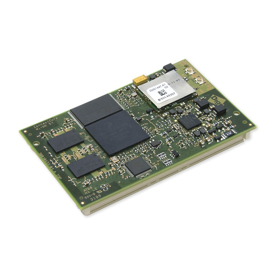
- Page 1 ConnectCore for i.MX51 Hardware Reference 90001128_F 4/7/2011...
- Page 2 Information in this document is subject to change without notice and does not represent a commitment on the part of Digi International. Digi provides this document “as is,” without warranty of any kind, either expressed or implied, including, but not limited to, the implied warranties of fitness or merchantability for a particular purpose. Digi may make improvements and/or changes in this manual or in the product(s) and/or the program(s) described in this manual at any time.
-
Page 3: Table Of Contents
C ................43 Video Subsystem ............. 44 Video Processing Unit (VPU) ..........44 Image Processing Unit (IPU) ..........46 Keypad ................ 48 Memory Cards ..............48 PWM ................49 RTC ................50 SPDIF ................50 SPI ................51 © 2011 Digi International, Inc. 3... - Page 4 WLAN, LE12 ..............65 WLAN, LE12 ..............66 Power LEDs, LE3, LE4, LE6 and LE7........66 User LEDs, LE49 and LE51 ..........66 Serial Status LEDs ............66 UART 1 Status LEDs ............67 UART 2 Status LEDs ............67 © 2011 Digi International, Inc. 4...
- Page 5 Peripheral Application Header, P21 ........100 Power-Over-Ethernet (PoE) - IEEE802.3af ....... 102 The PoE Module ............103 PoE Connector (power in), P17 .......... 103 PoE Connector (power out), P18 ........104 Main Power Connector ............105 SD-Card Interface............106 © 2011 Digi International, Inc. 5...
- Page 6 Analog Video Interface ............. 117 Analog Video Connector, X32 ..........118 WLAN Interface .............. 119 Antenna Connectors (WLAN) ..........120 Digi XBee Interface ............121 Digi XBee Module Connectors, X28 and X29 ......122 A p p e n d i x A : M o d u l e S p e c i f i c a t i o n s ..1 2 3 Mechanical Specifications ..........
- Page 7 A p p e n d i x D : C h a n g e L o g ....1 5 0 Revision A ..............150 Revision B ..............150 Revision C ..............150 Revision D..............150 Revision E ..............151 Revision F ..............151 © 2011 Digi International, Inc. 7...
- Page 8 Filenames, pathnames, and code examples. Digi Information Document Updates Please always check the product specific section on the Digi support website at www.digiembedded.com/support for the most current revision of this document. Contact Information For more information about your Digi products, or for customer service and technical support, contact Digi International.
-
Page 9: Chapter 1: About The Module
Complete and cost-efficient Digi JumpStart Kits for Microsoft Windows Embedded CE 6.0 and Linux allow immediate and professional embedded product development with dramatically reduced design risk and time-to-market. -
Page 10: Features And Functionality
– Up tp 3x USB 2.0 High-Speed USB Host ports – 1 USB 2.0 On-The-Go USB port (with integrated PHY on module) 1-wire Keypad 6x4 Two independent PWM interfaces 8, 16-bit External Memory interface © 2011 Digi International, Inc. 10... -
Page 11: Module Variant
Complete Microsoft Windows Embedded CE 6.0 and Linux platform support with full source code Module Variant The ConnectCore for i.MX51 module is available with various population options such as network interfaces (Ethernet, WLAN), memory (flash, RAM), processor (speed grade/ operating temperature) and others. © 2011 Digi International, Inc. 11... -
Page 12: Block Diagram
UART x 3 Resizing & Blending USB OTG Host + PHY CSPI HS x 2 / LS x 1 Inversion & Rota on Inversion & Rota on USB Host x 3 SPDIF Tx Dual-Camera Interface Fuse Box 10/100 Ethernet x © 2011 Digi International, Inc. 12... -
Page 13: Module
NAND & Memory Interf es Interf ces E ernet MC13892 C 3892 Controller ery Mgmt Buck Switc es WLAN 10-bit ADC LDO Regul or Touc I/F Boost Switc Power Supply RTC / Osc CPU I/F Accelerometer 180-pin Connector © 2011 Digi International, Inc. 13... -
Page 14: Module Pinout
CSI1_D19 Camera 1 data GPIO27 CSI1_VSYNC/GPIO3_14 i.MX51: CSI1_VSYNC Camera 1 vertical synchronization GPIO27 CSI1_HSYNC/GPIO3_15 i.MX51: CSI1_HSYNC Camera 1 horizontal synchronization GPIO27 CSI1_PIXCLK i.MX51: CSI1_PIXCLK Camera 1 pixel clock GPIO27 CSI1_MCLK i.MX51: CSI1_MCLK Camera 1 & 2 Master clock © 2011 Digi International, Inc. 14... - Page 15 PMIC_INT_REQ Reserved This high-priority interrupt input on i.MX51 is not used. The output interrupt from PMIC is connected to standard interrupt GPIO_5 on i.MX51. PMIC_PWGTDRV PWRGTDRV1 MC13892: PWRGTDRV1 Not used PMIC_LED CHRGLED MC13892: CHRGLED Battery Charging LED © 2011 Digi International, Inc. 15...
- Page 16 ETH_PHY: RXD4 HSGPIO27 DISP2_DATA4 i.MX51: DISP2_DATA4 LCD2 Data HSGPIO27 DISP2_DATA3 i.MX51: DISP2_DATA3 LCD2 Data GPIO27 DISP2_DATA6/ i.MX51: DISP2_DATA6 LCD2 Data Ethernet 1 and LCD2 cannot MII_TXD1/USBH3_STP be used at the same time. ETH_PHY: TXD1 © 2011 Digi International, Inc. 16...
- Page 17 ETH_PHY: RXD1 IOR_BACK i.MX51: IOR_BACK Not used GPIO27 DI2_PIN3/MII_MDIO i.MX51: DI2_PIN3 LCD2 Data Ethernet 1 and LCD2 cannot be used at the same time. ETH_PHY: MDIO i.MX51: IOB Not useD i.MX51: IOG Not used IOB_BACK i.MX51: IOB_BACK Not used © 2011 Digi International, Inc. 17...
- Page 18 ETH2_LINK# ETH_CTRL: GPIO0/LED1# Ethernet 2 Link LED GPOIO18 EIM_CS0/GPIO2_25 i.MX51: EIM_CS0 Peripheral Application Chip Select GPOIO18 EIM_CS1/GPIO2_26 i.MX51: EIM_CS1 Not used GPOIO18 EIM_CS2/GPIO2_27/ i.MX51: EIM_CS2 Not used FEC_RDATA2/SISG5/ CSI1_D4/AUD5_TXD GPOIO18 EIM_CS3/GPIO2_28/ i.MX51: EIM_CS3 Not used FEC_RDATA3/ SSI_EXT2_CLK/ CSI1_D5/AUD5_RXD © 2011 Digi International, Inc. 18...
- Page 19 Peripheral Application Data / Address GPOIO18 EIM_DA10/TRACE26 i.MX51: EIM_DA10 Not used GPOIO18 EIM_DA11/TRACE27 i.MX51: EIM_DA11 Not used GPOIO18 EIM_DA13/TRACE29 i.MX51: EIM_DA13 Not used GPOIO18 EIM_DA12/TRACE28 i.MX51: EIM_DA12 Not used GPOIO18 EIM_DA15/TRACE31 i.MX51: EIM_DA15 Not used GPOIO18 EIM_DA14/TRACE30 i.MX51: EIM_DA14 Not used © 2011 Digi International, Inc. 19...
- Page 20 ETH_CTRL: D7 SPDIF_OUT1/ AUD4_TXFS/TRACE7 GPOIO18 EIM_D22/GPIO2_6/ i.MX51: EIM_D22 Peripheral Application Data USBH2_DATA6/ ETH_CTRL: D8 AUD4_TXC/TRACE6 GPOIO18 EIM_D24/GPIO2_8/ i.MX51: EIM_D24 Peripheral Application Data UART3_CTS#/ ETH_CTRL: D8 I2C2_SDA/AUD6_RXFS/ TRACE8 GPOIO18 EIM_D25/KEY_COL6/ i.MX51: EIM_D25 Peripheral Application Data UART3_RXD/ ETH_CTRL: D9 UART2_CTS#/ CMPOUT1/TRACE9 © 2011 Digi International, Inc. 20...
- Page 21 EIM_A25 Not used USBH2_DIR/DI1_PIN4 GPOIO18 EIM_A24/GPIO2_18/ i.MX51: EIM_A24 Not used USBH2_CLK GPOIO18 EIM_A27/GPIO2_21/ i.MX51: EIM_A27 XBEE_SLEEP_RQ USBH2_NXT/SISG1/ CSI2_DATA_EN/ DI1_PIN1 GPOIO18 EIM_A26/GPIO2_20/ i.MX51: EIM_A26 Not used USBH2_STP/SISG0/ CSI1_DATA_EN/ DI2_EXT_CLK GPOIO18 EIM_OE#/GPIO2_24 i.MX51: EIM_OE Peripheral Application Output Enable ETH_CTRL: RD# © 2011 Digi International, Inc. 21...
-
Page 22: J2 Pinout
DISP1_DAT4 HDMI, VGA and LCD1 Data HSGPIO27 DISP1_DAT5 i.MX51: DISP1_DAT5 HDMI, VGA and LCD1 Data GPIO27 DISP1_DAT6 i.MX51: DISP1_DAT6 HDMI, VGA and LCD1 Data, Boot Configuration GPIO27 DISP1_DAT7 i.MX51: DISP1_DAT7 HDMI, VGA and LCD1 Data, Boot Configuration © 2011 Digi International, Inc. 22... - Page 23 LCD1 and LCD2 GPIO2 GPIO27 DI1_PIN3 i.MX51: DI1_PIN3 HDMI, VGA and LCD1 VSYNC GPIO27 DI1_PIN15 i.MX51: DI1_PIN15 HDMI, VGA and LCD1 DRDY GPIO27 DI1_PIN12/GPIO3_1 i.MX51: DI1_PIN12 LCD2 PWREN# GPIO27 DI_GP2 i.MX51: DI_GP2 Not used GPIO27 DI_GP1 i.MX51: DI_GP1 Not used © 2011 Digi International, Inc. 23...
- Page 24 Not used VSWLED GPIO27 CSI2_D12/GPIO4_9 i.MX51: CSI2_D12 Camera 2 Data GPIO27 CSI2_D13/GPIO4_10 i.MX51: CSI2_D13 Camera 2 Data HSGPIO27 CSI2_D14 i.MX51: CSI2_D14 Camera 2 Data HSGPIO27 CSI2_D15 i.MX51: CSI2_D15 Camera 2 Data HSGPIO27 CSI2_D16 i.MX51: CSI2_D16 Camera 2 Data © 2011 Digi International, Inc. 24...
- Page 25 UHVIO33 SD2_CLK/I2C1_SDA/ i.MX51: SD2_CLK Reserved In modules without WLAN SPI_SCLK WLAN: SDIO_CLK this SD bus can be used in the development boards. UHVIO33 SD2_DATA1/ i.MX51: SD2_DATA1 Reserved SD1_DATA5 WLAN: SDIO_DATA1 UHVIO33 SD2_CMD/I2C1_SCL/ i.MX51: SD2_CMD Reserved SPI_MOSI WLAN: SDIO_CMD © 2011 Digi International, Inc. 25...
- Page 26 GPIO1_4 Reserved HDMI Interrupt and PMIC Watchdog input cannot be used at the same time. UHVIO31 SD1_DATA3/ i.MX51: SD1_DATA3 MicroSD Data AUD5_TXFS/SPI_SS1 GPIO27 CSPI1_MOSI/I2C1_SDA/ i.MX51: CSPI1_MOSI SPI_MOSI GPIO4_22 MC13892: MOSI GPIO27 CSPI1_SS0_PMIC/ i.MX51: CSPI1_SS0 Reserved AUD4_TXC/GPIO4_24 MC13892: CS © 2011 Digi International, Inc. 26...
- Page 27 USBH1_DIR/SPI_MOSI/ i.MX51: USBH1_DIR USB Host GPIO1_26/I2C2_SDA GPIO27 USBH1_DATA3/ i.MX51: USBH1_DATA3 USB Host (default) and UART2 UART2_RTS#/GPIO1_14 Console GPIO27 USBH1_STP/SPI_RDY/ i.MX51: USBH1_STP USB Host GPIO1_27 GPIO27 USBH1_DATA5/ i.MX51: USBH1_DATA5 USB Host UART2_RTS#/GPIO1_14 GPIO27 USBH1_NXT/SPI_MISO/ i.MX51: USBH1_NXT USB Host GPIO1_28 © 2011 Digi International, Inc. 27...
- Page 28 NANDF_D6/PATA_D6/ i.MX51: NANDF_D6 Reserved SD4_LCTL/GPIO4_2 NAND_FLASH: I/O6 UHVIO31 NANDF_D5/PATA_D5/ i.MX51: NANDF_D5 Reserved SD4_WP/GPIO4_3 NAND_FLASH: I/O5 UHVIO31 NANDF_D8/PATA_D8/ i.MX51: NANDF_D8 SD/MMC Data GPIO4_0/SD3_DATA0 UHVIO31 NANDF_D7/PATA_D7/ i.MX51: NANDF_D7 Reserved GPIO4_1 NAND_FLASH: I/O7 UHVIO31 NANDF_D10/ i.MX51: NANDF_D10 SD/MMC Data PATA_D10/GPIO3_30/ SD3_D2 © 2011 Digi International, Inc. 28...
- Page 29 SD/MMC Clock SD clock and Digital IO cannot be used at the same time. UHVIO31 NANDF_WE#/ i.MX51: NANDF_WE_B Reserved PATA_DIOW/GPIO3_3 NAND_FLASH: WE# UHVIO31 GPIO_NAND/ i.MX51: GPIO_NAND SD/MMC Card Detect PATA_INTRQ/GPIO3_12 UHVIO31 NANDF_ALE/ i.MX51: NANDF_ALE Reserved PATA_BUFFER_EN/ NAND_FLASH: ALE GPIO3_5 © 2011 Digi International, Inc. 29...
- Page 30 User LED2 and Digital I/O PATA_IORDY/GPIO3_9 Connector NAND_FLASH: NC UHVIO31 NANDF_RB0/ i.MX51: NANDF_RB0 Reserved PATA_DMARQ/GPIO3_8 NAND_FLASH: R/B# UHVIO31 NANDF_RB3/GPIO3_11 i.MX51: NANDF_RB3 Digital I/O Connector NAND_FLASH: NC UHVIO31 NANDF_RB2/GPIO3_10 i.MX51: NANDF_RB2 User LED1 and Digital I/O Connector NAND_FLASH: NC © 2011 Digi International, Inc. 30...
-
Page 31: Power
The battery charger supply is used to charge rechargeable batteries, as well as to power up the module when there is no battery or the battery is discharged. The minimum voltage of the battery charger is +3.4V. The maximum voltage of the battery charger is +20V. © 2011 Digi International, Inc. 31... -
Page 32: Supply Outputs
The maximum current provided by this supply is 100mA. The current available to supply off-module components is 50mA. S W B T ( + 5 V ) The voltage level of the SWBT supply is +5V. The maximum current provided by this supply is 300mA. © 2011 Digi International, Inc. 32... -
Page 33: Mc13892 Power Management
The following figure shows the block diagram of the MC13892. MC13892 Battery 4 Buck 12 LDO Backlight Management Switchers Regulators Drivers Bias & +5V Boost 10 Bit ADC References Switcher Drivers Touch Screen Power Interface Control Logic Control 32.768KHz Processor Logic Interfacing Interface © 2011 Digi International, Inc. 33... -
Page 34: Memory
External CS0# 0xB7FF_FFFF EIM_CS1 0xB800_000- 128M External CS1# 0xBFFF_FFFF EIM_CS2 0xC000_000- 128M External CS2# 0xC7FF_FFFF EIM_CS3 0xC800_000- External CS3# 0xCBFF_FFFF EIM_CS4 0xCC00_000- External CS4# 0xCDFF_FFFF EIM_CS5 0xCE00_000- 32M (minus 64K) External CS5# Used for Ethernet Controller on module 0xCFFE_FFFF © 2011 Digi International, Inc. 34... -
Page 35: Multiplexed Gpio
GPIO1_14 ALT2 USBH1_DATA3 USB Host GPIO1_15 ALT2 USBH1_DATA4 USB Host GPIO1_16 ALT2 USBH1_DATA5 USB Host GPIO1_17 ALT2 USBH1_DATA6 USB Host GPIO1_18 ALT2 USBH1_DATA7 USB Host GPIO1_19 ALT5 DISP2_DAT6 Ethernet 1 GPIO1_20 ALT3 UART2_RXD UART2_RXD GPIO1_21 ALT3 UART2_TXD UART2_TXD © 2011 Digi International, Inc. 35... - Page 36 EIM_A19 GPIO GPIO2_14 ALT1 EIM_A20 GPIO GPIO2_15 ALT1 EIM_A21 GPIO GPIO2_16 ALT1 EIM_A22 GPIO GPIO2_17 ALT1 EIM_A23 GPIO GPIO2_18 ALT1 EIM_A24 GPIO GPIO2_19 ALT1 EIM_A25 GPIO GPIO2_20 ALT1 EIM_A26 GPIO GPIO2_21 ALT1 EIM_A27 XBEE_SLEEP_RQ GPIO2_22 ALT1 EIM_EB2 EIM_EB2 © 2011 Digi International, Inc. 36...
- Page 37 NANDF_RB1 GPIO / User LED2 GPIO3_10 ALT3 NANDF_RB2 GPIO / User LED1 GPIO3_11 ALT3 NANDF_RB3 GPIO GPIO3_12 ALT3 CSI1_D8 Not used ALT0 GPIO_NAND Card Detect input SD Card GPIO3_13 ALT3 CSI1_D9 Camera 1 Reset GPIO3_14 ALT3 CSI1_VSYNC CSI1_VSYNC © 2011 Digi International, Inc. 37...
- Page 38 NANDF_D0 NANDF_D0 GPIO4_7 ALT3 NANDF_D1 NANDF_D1 GPIO4_8 ALT3 NANDF_D0 NANDF_D0 GPIO4_9 ALT3 CSI2_D12 CSI2_D12 GPIO4_10 ALT3 CSI2_D13 CSI2_D13 GPIO4_11 ALT3 CSI2_D18 CSI2_D18 GPIO4_12 ALT3 CSI2_D19 CSI2_D19 GPIO4_13 ALT3 CSI2_VSYNC CSI2_VSYNC GPIO4_14 ALT3 CSI2_HSYNC CSI2_HSYNC GPIO4_15 ALT3 CSI2_PIXCLK CSI2_PIXCLK © 2011 Digi International, Inc. 38...
- Page 39 GPIO4_24 ALT3 CSPI1_SS0 CSPI1_SS0 (MC13892 Chip select) GPIO4_25 ALT3 CSPI1_SS1 CSPI1_SS1 GPIO4_26 ALT3 CSPI1_RDY LCD SPI chip select GPIO4_27 ALT3 CSPI1_SCLK CSPI1_SCLK GPIO4_28 ALT3 UART1_RXD UART1_RXD GPIO4_29 ALT3 UART1_TXD UART1_TXD GPIO4_30 ALT3 UART1_RTS UART1_RTS GPIO4_31 ALT3 UART1_CTS UART1_CTS © 2011 Digi International, Inc. 39...
-
Page 40: Interfaces
Resolution: 10-bit Differential linearity error: 1 LSB Integral linearity error: 3 LSB Conversion time per channel: 10 us Low power consumption (1 mA of conversion current) Analog input range: 0 ~ 2.4V © 2011 Digi International, Inc. 40... -
Page 41: Synchronous Serial Interface (Ssi)
S, LSB, MSB aligned Programmable word length 8, 10, 12, 16, 18, 20, 22 or 24 bits Program options for frame sync and clock generation Programmable I S modes (Master, Slave or Normal) AC97 support © 2011 Digi International, Inc. 41... -
Page 42: External Memory Interface (Emi)
The module also provides two status signals for activity and link LEDs. Ethernet 2 The ConnectCore for i.MX51 module can provide a high-performance 10/100Mbit Ethernet controller (LAN9221) with integrated MAC and PHY from SMSC as a second Ethernet port. © 2011 Digi International, Inc. 42... - Page 43 – J2.111 - SPI1_MOSI (used on the module as communication channel for Freescale PMIC) – J2.86 - SD2_CLK (used on the module as communication channel for Wireless LAN interface, if present) C1_SCL: – J1.144 - EIM_D19 (used on the module for external Ethernet controller, if present) © 2011 Digi International, Inc. 43...
-
Page 44: Video Subsystem
– MPEG-4 decoder for simple profile, advanced simple profile except GMC – H.263 decoder for baseline profile – Divx Home Theater decoder for profile (version 3.x, 4.x, 5.x, 6.x) and Xvid – MPEG-2 decoder for main profile @ high level – RV decoder for profile 8/9/10 © 2011 Digi International, Inc. 44... - Page 45 – Multiple codec: supports up to 4 decoding/encoding processes simultaneously, each process can have a different format Other features – Supports rotating and mirroring simultaneously. – Built-in de-ringing filter – Built-in de-blocking filter for MPEG-2/MPEG-4/Divx – Simultaneous multi-stream and multi-standard processing capability – Robust error detection © 2011 Digi International, Inc. 45...
-
Page 46: Image Processing Unit (Ipu)
The following figure shows the simplified block diagram of the IPU: Image Processing Unit (IPU) SMFC Camera Sensor I/F Camera Sensor I/F Video De Interlacer Display I/F Image Converter IDMAC Display I/F Image DMA Controller Display processor DMFC Display Control Control Module Image Rotator © 2011 Digi International, Inc. 46... - Page 47 – Controls FIFOs for output from the CSIs to system memory Display Multi FIFO Controller - DMFC – Controls FIFOs for IDMAC channels related to the display system Control Module - CM – Provides control and synchronization © 2011 Digi International, Inc. 47...
-
Page 48: Keypad
The main features of the Memory Card interfaces are the following: Designed to work with MMC, MMC plus, MMC RS, SD memory, miniSD memory, SDIO, and SD Combo. Compatible with the following specifications: – MMC System Specification Version 4.2 – SD Host Controller Standard Specification Version 2.0 © 2011 Digi International, Inc. 48... -
Page 49: Pwm
12-bit prescaler for division of clock Sound and melody generation Active high or active low configured output Can be programmed to be active in low power and debug modes Interrupts at compare and rollover © 2011 Digi International, Inc. 49... -
Page 50: Rtc
SPDIF transmitter, the IEC958 biphase bit stream is generated on both edges of the SPDIF transmit clock. IEC 60958 format SPIDF output 7 transmit clock source Consumer channel status support Support for interrupt and DMA © 2011 Digi International, Inc. 50... -
Page 51: Spi
Programmable interrupt generation prior to time-out Programmable time duration between interrupt and timeout events, from 0 to 128 seconds in steps of 0.5 seconds Power down counter enabled out of any reset by default © 2011 Digi International, Inc. 51... -
Page 52: Uart
High-speed ULPI transceiverless link logic (HS-TLL) for onboard connection to a high- speed ULPI interface USB peripheral Main features of the USB OTG interface: High-speed OTG HS/FS ULPI compliant interface Software configurable for ULPI or serial transceiver interface © 2011 Digi International, Inc. 52... -
Page 53: Wlan
P/N U.FL-LP-N-2 or U.FL-LP(V)-N-2) is strongly recommended to avoid damage to the U.FL connectors on the module. To mate U.FL connectors, the mating axes of both connectors must be aligned. The "click" will confirm mated connection. Do not attempt insertion at an extreme angle. © 2011 Digi International, Inc. 53... -
Page 54: Cable Specification: U.fl/W.fl To Rp-Sma
Note: 1 = U.FL 2 = RP-SMA This module obtained its complete certification by using the cable described here. End Note: users in North America should use a cable that matches these specifications to maintain the module’s certification. © 2011 Digi International, Inc. 54... -
Page 55: Chapter 2: About The Development Board
Screw-flange Battery header with enable jumper 3V coin cell battery Connectors for Digi 802.3af PoE Application board (sold separately) 1 x UART RS232 with status LEDs and SUB-D 9-pin connector 1 x UART MEI (RS232/RS4xx) with status LEDs and SUB-D 9-pin connector ... - Page 56 XBee interface (XBee module sold separately) Peripheral application header Module Expansion connectors JTAG interface 2 x User LEDs (green) 2 x User Push-buttons 1 x Power down Push-button 1 x Reset Push-button © 2011 Digi International, Inc. 56...
-
Page 57: The Development Board
ConnectCore f or i .M X 5 1 The Development Board © 2011 Digi International, Inc. 57... -
Page 58: Switches And Push-Buttons
The development board has an ON/OFF switch, S2. The power switch S2 can switch both 9V-30VDC input power supply and 12VDC coming out of the optional PoE module. However, if a power plug is connected to the DC power jack, the PoE is disabled. © 2011 Digi International, Inc. 58... -
Page 59: Reset Button, S4
GPIO3_6 is used in User Button S3 and also in the Digital I/O connector for Digital I/O7. Ident Button, S10 The Ident push-button S10 is associated to the commissioning input of the Digi XBee modules. This input provides a variety of simple functions to aid in deploying devices in a network. For a deeply description of this functionality please refer to the Digi XBee modules documentation. -
Page 60: Uart 1 Switch, S6
UART will be in shutdown mode. S7.2 On = Shutdown Shutdown is the highest priority functionality. If switch S7.2 = ON, the UART 2 will be in Off = Normal Operation shutdown mode independently of the position of S7.1. © 2011 Digi International, Inc. 60... -
Page 61: Boot Configuration Switches, S8 And S9
On / Off Internal Boot configured by fuse block S9.1 / S9.2 On / On Serial downloader For a detailed description of the ConnectCore for i.MX51 boot mode functionality please refer to the Freescale i.MX51 Processor Hardware Reference Manual. © 2011 Digi International, Inc. 61... -
Page 62: Jumpers
Source, P29 UART/XBee, J30 & J31 LED 1, J16 WLAN Disable, J17 Button 1, Button 2, LED 2, Battery Enable, J5 When J5 is set, the development board can be powered by an external battery connected to J23. © 2011 Digi International, Inc. 62... -
Page 63: Module Power Source, P29
(on module) is configured for the LCD 2 interface. When removed, an internal touch screen controller is configured for the LCD 2 interface, and the internal analog touch screen controller (on module) is configured for the LCD 1 interface. © 2011 Digi International, Inc. 63... -
Page 64: Coincell Enable, J3
When set, this jumper supplies the real time clock with +3V from the lithium coin cell battery, even if the board is switched off. JTAG Mod., J4 When set, this jumper disables the JTAG interface for the ConnectCore for i.MX51. When removed, the JTAG interface is enabled. © 2011 Digi International, Inc. 64... -
Page 65: Leds
ConnectCore f or i .M X 5 1 LEDs +3.3V_JS, 9V-30V, +5V_JS, Batt, UART 2 Status LEDs UART 1 Status LEDs USER LED1, USER LED2, WLAN, LE12 Assoc., LE51 LE49 LED50 WLAN, LE12 LED indicating WLAN operational status. © 2011 Digi International, Inc. 65... -
Page 66: Wlan, Le12
2. The LEDs are connected to the TTL side of the RS232 or RS4xx transceivers. Green means corresponding signal high Red means corresponding signal low The intensity and color of the LED will change when the voltage is switching © 2011 Digi International, Inc. 66... -
Page 67: Uart 1 Status Leds
CTS# XBee Assoc., LE50 This LED is connected to the Associate output of the Digi XBee module. This LED provides information of the device's network status and diagnostics information. For a more in-depth description of this LED please refer to the Digi XBee modules documentation available at www.digi.com. -
Page 68: Audio Interface
This audio CODEC is controlled through the I C port 2 of the ConnectCore for i.MX51. Digital audio data is sent/received between the audio CODEC and the ConnectCore for i.MX51 through an I S interface (AUD3 channel of the i.MX51 AUDMUX). © 2011 Digi International, Inc. 68... -
Page 69: Line-Out Connector Pinout, J18
Three stereo audio jacks are provided on the development board: J18 connector for LINE+OUT J12 connector for LINE+IN J15 connector for microphone Line-out Connector Pinout, J18 Signal LINE-OUT-RIGHT LINE-OUT-LEFT HEADPHONE-DETECT Line-in Connector Pinout, J12 Signal LINE-IN-RIGHT LINE-IN-LEFT Microphone Connector Pinou, J15 Signal MIC-IN MICBIAS © 2011 Digi International, Inc. 69... -
Page 70: Coin Cell Battery
Keystone 1065 Renata CR2032N Ettinger 15.61.602 Panasonic CR2032N The development board provides a coin cell battery to back up the module’s integrated RTC while main power is disconnected. Jumper J3 controls if the coin cell battery power is available. © 2011 Digi International, Inc. 70... -
Page 71: Camera Interfaces
ConnectCore for i.MX51 CPU. The I C bus of the ConnectCore for i.MX51CPU is used to configure and control the two cameras. The I C device addresses of the Digi camera application kits (CC-ACC0MT9V111) are the following: Interface C Address (7 bits) -
Page 72: X15 Pinout
ConnectCore f or i .M X 5 1 Two 2 x 10 pin headers, X15 and X17, are provided on the development board for connecting two Digi camera application kits (optional) or customer specific hardware. X15 connector for camera 1 ... -
Page 73: Digital Io Interface
ConnectCore f or i .M X 5 1 Digital IO Interface Digital I/O Connector, X45 © 2011 Digi International, Inc. 73... -
Page 74: Digital I/O Connector, X45
On the development board, GPIO3_6 is connected to USER_KEY1. When using this signal as digital I/O, the USER_KEY1 should not be used. The digital I/O interface is not protected against ESD, over voltage or inverse polarity. Note: Care must be taken when using these signals. © 2011 Digi International, Inc. 74... -
Page 75: Ethernet 1 Interface
LEDs for the Ethernet 1 interface. This interface is attached to the Fast Ethernet controller (FEC) of the i.MX51. The ConnectCore for i.MX51 module provides a 10/100 Ethernet PHY chip for this interface. The Ethernet 1 RJ-45 connector also supports 802.3af (PoE). © 2011 Digi International, Inc. 75... -
Page 76: Ethernet 1, Rj-45 Connector X7
The table below shows the description of the Ethernet 1 LEDs. Description Yellow Network activity (speed): Flashing - indicates network traffic Off - no network traffic Green Network link: On - indicates an active network link Off - no network link present © 2011 Digi International, Inc. 76... -
Page 77: Ethernet 2 Interface
Ethernet 2 Interface Ethernet 2 Connector, J27 The development board provides a 2x20 expansion connector for connecting an optional Digi Ethernet adapter board (100M_ETHADPT) or customer specific setup. The Ethernet 2 interface is provided by an optional on-module Ethernet MAC/PHY. -
Page 78: Ethernet 2, Connector J17
ConnectCore f or i .M X 5 1 Ethernet 2, Connector J17 The table below shows the pinout of the Ethernet 2 expansion connector. Signal Signal ETH2_TX+ ETH2_RX+ ETH2_TX- ETH2_RX- Reserved (ETH2_DC+) Reserved (ETH2_DD+) Reserved (ETH2_DC-) Reserved (ETH2_DD-) ETH2_ACTIVITY# ETH2_LINK# © 2011 Digi International, Inc. 78... -
Page 79: Hdmi Interface
The development board provides an HDMI interface connected to the display interface 1 of the ConnectCore for i.MX51 CPU. An Analog Devices AD9389 HDMI transmitter is used in the development board. This HDMI transmitter is controlled through the I C port 2 of the ConnectCore for i.MX51. © 2011 Digi International, Inc. 79... -
Page 80: Hdmi Connector, J19
The development board provides an HDMI connector, J19. THe HDMI interface is connected to the Display 1 interface of the ConnectCore for i.MX51 CPU. The table below shows the pinout of the HDMI connector: Signal HDMI_TX2+ HDMI_TX2- HDMI_TX1+ HDMI_TX1- HDMI_TX0+ HDMI_TX0- HDMI_TXC+ HDMI_TXC- HDMI_SCL HDMI_SDA HOTPLUG_DET © 2011 Digi International, Inc. 80... -
Page 81: I 2 C Interface
ConnectCore f or i .M X 5 1 C Interface I C Header, © 2011 Digi International, Inc. 81... -
Page 82: I 2 C Header, P22
C port 2 is connected to the following headers/interfaces on the development board. Interface C Address (7 bits) C Header Camera 1 0 x 5 C (Digi CC-ACC-MT9V111) Camera 2 0 x 4 8 (Digi CC-ACC-MT9V111) HDMI Transmitter 0 x 39... -
Page 83: Jtag Interface
ConnectCore f or i .M X 5 1 JTAG Interface JTAG Interface, X13 © 2011 Digi International, Inc. 83... -
Page 84: Standard Jtag Arm Connector, X13
(ICS) such as Ronetix PEEDI or other. Function Function +1.8V +3.3V JTAG_TRST# JTAG_TDI JTAG_TMS JTAG_TCK Reserved (RTCK) JTAG_TDO JTAG_RESET# JTAG_DE# In order to enable ETM functionality, Digi offers an optional ETM adapter board (sold Note: separately, Digi P/N CC-ACC-MX51-ETM). Please contact us. © 2011 Digi International, Inc. 84... -
Page 85: Lcd Interfaces
LCD2 Connector, P2 LCD1 Connector, P1 The development board provides two 2x40 pin, 1.27mm connectors for accessing a Digi- provided LCD application boards (CC-ACC0LCDW-70) or a user defined LCD application board. P1 : corresponds to i.MX51 display interface 1 ... -
Page 86: Lcd 1 Connector, P1
LCD1_DATA14 (R4) LCD1_DATA215(R5) LCD1_DATA16 (R6) LCD1_DATA17 (R7) LCD1_DATA10 (G0) LCD1_DATA11 (G1) LCD1_DATA6 (G2) LCD1_DATA7 (G3) LCD1_DATA8 (G4) LCD1_DATA9 (G5) LCD1_DATA10 (G6) LCD1_DATA11 (G7) LCD1_DATA4 (B0) LCD1_DATA5 (B1) LCD1_DATA0 (B2) LCD1_DATA1 (B3) LCD1_DATA2 (B4) LCD1_DATA3 (B5) LCD1_DATA4 (B6) LCD1_DATA75 (B7) © 2011 Digi International, Inc. 86... - Page 87 ConnectCore f or i .M X 5 1 Function Function LCD1_BIAS LCD1_PCLK LCD1_PWREN# LCD1_VSYNC LCD1_HSYNC TOUCH_X1 TOUCH_Y1 TOUCH_X2 TOUCH_Y2 _SDA _SCL LCD_SPI_SS# SPI1_CLK SPI1_MOSI SPI1_MISO RESET# LCD1_TOUCH_INT/EXT# LCD1_GPIO1 LCD1_GPIO2 LCD_PENIRQ +3.3V +3.3V +9-30V +9-30V +9-30V +9-30V © 2011 Digi International, Inc. 87...
-
Page 88: Lcd 2 Connector, P2
LCD2_DATA15 (R5) LCD2_DATA16 (R6) LCD2_DATA17 (R7) LCD2_DATA10 (G0) LCD2_DATA11 (G1) LCD2_DATA6 (G2) LCD2_DATA7 (G3) LCD2_DATA8 (G4) LCD2_DATA9 (G5) LCD2_DATA10 (G6) LCD2_DATA11 (G7) LCD2_DATA4 (B0) LCD2_DATA5 (B1) LCD2_DATA0 (B2) LCD2_DATA1 (B3) LCD2_DATA2 (B4) LCD2_DATA3 (B5) LCD2_DATA4 (B6) LCD2_DATA5 (B7) © 2011 Digi International, Inc. 88... - Page 89 ConnectCore f or i .M X 5 1 Function Function LCD2_BIAS LCD2_PCLK LCD2_PWREN# LCD2_VSYNC LCD2_HSYNC TOUCH_X1 TOUCH_Y1 TOUCH_X2 TOUCH_Y2 _SDA _SCL LCD_SPI_SS# SPI1_CLK SPI1_MOSI SPI1_MISO RESET# LCD2_TOUCH_INT/EXT# LCD2_GPIO1 LCD2_GPIO2 LCD_PENIRQ +3.3V +3.3V +9-30V +9-30V +9-30V +9-30V LED_BCK+ LED_BCK- © 2011 Digi International, Inc. 89...
-
Page 90: Microsd™ Card Interface
ConnectCore f or i .M X 5 1 MicroSD Card Interface ™ MicroSD Connector, X14 © 2011 Digi International, Inc. 90... -
Page 91: Microsd™ Connector, X14
(pin-9 and pin-10 are connected to chassis). A hot-plug insertion or removal is not possible with this connector. The following table shows the pinout of the MicroSD™ connector: Signal SD_SATA2 SD_DATA3 SD_CMD +3.3V SD_CLK SD_DATA0 SD_DATA1 SD_CD (Connected to chassis) SD_CD (Connected to chassis) © 2011 Digi International, Inc. 91... -
Page 92: Module Connectors And Signal Rails
ConnectCore f or i .M X 5 1 Module Connectors and Signal Rails Signal Rail 2, J26 Module Connector, Module Connector, Signal Rail 1, J25 © 2011 Digi International, Inc. 92... -
Page 93: Module Connectors
CSI1_D10 CSI1_D11 CSI1_D12 CSI1_D13 CSI1_D14 CSI1_D15 CSI1_D16 CSI1_D17 CSI1_D18 CSI1_D19 CSI1_VSYNC/GPIO3_14 CSI1_HSYNC/GPIO3_15 CSI1_PIXCLK CSI1_MCLK WLAN_TDO WLAN_TCK WLAN_TDI WLAN_TMS WLAN_LED RS_BT_PRIORITY RS_WLAN_ACTIVE RS_BT_ACTIVE +2.775V WLAN_DISABLE# +2.775V +2.775V MC13892_GPO1 +2.775V PMIC_PWRON1 PMIC_STDBY_REQ PMIC_INT_REQ PWRGTDRV1 CHRGLED PWRGTDRV2 CHRGSE1# VCC_COINCELL VLIO +5V_IN © 2011 Digi International, Inc. 93... - Page 94 D12_PIN4/MII_CRS D12_PIN3/MII_MDIO IOR_BACK IOG_BACK JTAG_TRST# IOB_BACK JTAG_MOD# JTAG_TCK JTAG_DE# JTAG_TMS RESET_IN# JTAG_TDI +1.8V JTAG_TDO EIM_CS1/GPIO2_26 POR# EIM_CS3/GPIO2_28 EIM_CS0/GPIO2_25 EIM_CS5_LAN9221_CS#/GPIO2_30 EIM_CS2/GPIO2_27 EIM_LBA/GPIO3_1 EIM_CS4/GPIO2_29 EIM_DA1/TRACE17 EIM_DTACK/GPIO2_31 EIM_DA3/TRACE19 EIM_DA0/TRACE16 EIM_DA5/TRACE21 EIM_DA2/TRACE18 EIM_DA7/TRACE23 EIM_DA4/TRACE20 EIM_DA9/TRACE25 EIM_DA6/TRACE22 EIM_DA11/TRACE27 EIM_DA8/TRACE 24 EIM_DA13/TRACE29 EIM_DA10/TRACE26 EIM_DA15/TRACE31 © 2011 Digi International, Inc. 94...
- Page 95 EIM_DA20/TRACE4 EIM_DA27/TRACE11 EIM_DA22/TRACE6 EIM_DA29/TRACE13 EIM_DA24/TRACE8 EIM_DA31/TRACE15 EIM_DA26/TRACE10 EIM_A17/GPIO2_11 EIM_DA28/TRACE12 EIM_A19/GPIO2_13 EIM_DA30/TRACE14 EIM_A21/GPIO2_15 EIM_A16/GPIO2_10 EIM_A23/GPIO2_17 EIM_A18/GPIO2_12 EIM_A25/GPIO2_19 EIM_A20/GPIO2_14 EIM_A27/GPIO2_21 EIM_A22/GPIO2_16 EIM_OE#/GPIO2_24 EIM_A24/GPIO2_18 EIM_RW# EIM_A26.GPIO2_20 EIM_CRE/GPIO3_2 EIM_EB0 EIM_WAIT EIM_EB1 EIM_EB2/GPIO2_22/TRCTL EIM_BCLK EIM_EB3/GPIO2_23/TRCLK NANDF_ALE/GPIO3_5 NAND_RE#/SD3_DATA1/GPIO3_4 NANDF_WP#/SD3_DATA2/GPIO3_7 NANDF_CLE/GPIO3_6 NANDF_RB1_SP12_RDY/GPIO3_9 NANDF_RB0/SD3_DATA3/GPIO3_8 NANDF_RB3/SP12_MISO/GPIO3_11 NANDF_R2/SP12_SCLK/GPIO3_10 © 2011 Digi International, Inc. 95...
-
Page 96: J26 Pinout
DISP1_DAT18 DISP1_DAT19 DISP1_DAT20 DISP1_DAT21 DISP1_DAT22 DISP1_DAT23 DI1_PIN2 DI1_DISP_CLK DI1_PIN11/GPIO3_0 DI1_PIN3 DI1_PIN13/GPIO3_2 DI1_PIN12/GPIO3_1 DI1_PIN15 DI_GP1 DI_GP2 DI_GP3/MII_TX_ER DI_GP4/MII_RXD2 DI1_D0_CS/GPIO3_3 DI1_D1_CS/GPIO3_4 ADIN5 TOUCH_X1 ADIN6 TOUCH_X2 ADIN7 TOUCH_Y1 ADC_GND TOUCH_Y2 ADTRIG SWBST LEDR LEDG LEDB CSI2_D12/GPIO4_9 CSI2_D13/GPIO4_10 CSI2_D14 CSI2_D15 CSI2_D16 CSI2_D17 © 2011 Digi International, Inc. 96... - Page 97 KEY_COL3 ROW3 KEY_COL5/UART3_CTS#/I2C2_SDA KEY_COL4/UART3_RTS#/I2C2_SCL GPIO1_0/SD1_CD#/SPI_SS2 OWIRE_LINE/GPIO1_24 GPIO1_1/SD1_WP#/SPI_MISO SC1_CMD/AUD5_RXFS/SPI_MOSI SD1_DAT0/AUD5_TXD/SPI_MOSI SD1_CLK/AUD5_RXC/SPI_SCLK SD1_DATA1/AUD5_RXD WDOG1#/GPIO1_4 SD1_DATA2/AUD5_TXC CSPI1_MOSI/I2C1_SDA/GPIO4_22 SD1_DATA3/AUD5_TXFS/SPI_SS1 CSPI1_MISO/AUD4_RXD/GPIO4_23 CSPI1_SS0_PMIC/AUD4_TXC/GPIO4_24 CSPI1_SCLK/I2C1_SDA/GPIO4_27 CSPI1_SS1/AUD4_TXD/GPIO4_25 UART1_RXD/GPIO4_28 CSPI1_RDY/AUD4_TXFS/GPIO4_26 UART1_TXD/PWM2/GPIO4_29 UART1_RTS#/GPIO4_30 UART2_RXD/GPIO1_20 UART1_CTS#/GPIO4_31 UART2_TXD/GPIO1_21 UART3_RXD/UART1_DTR#/GPIO1_22 USBH1_DATA2/UART2_TXD/GPIO1_13 UART3_TXD/UART1_DSR#/GPIO_23 USBH1_DATA4/SPI_SS0/GPIO1_15 USBH1_DATA0/UART2_CTS#/GPIO1_11 USBH1_DATA6/SPI_SS2/GPIO1_17 USBH1_DATA1/UART2_RXD/GPIO1_12 USBH1_DIR/SPI_MOSI/GPIO1_26/ USBH1_DATA3/UART2_RTS#/GPIO1_14 I2C2_SDA USBH1_STP/SPI_RDY/GPIO1_27 USBH1_DATA5/SPI_SS1/GPIO1_16 © 2011 Digi International, Inc. 97...
- Page 98 NANDF_D2/PATA_D2/SD4_DATA5/ NANDF_D1/PATA_D1/SD4_DATA6/ GPIO4_6 GPIO4_7 NANDF_D4/PATA_D4/SD4_CD/ NANDF_D3/PATA_D3/SD4_DATA4/ GPIO4_4 GPIO4_5 NANDF_D6/PATA_D6/SD4_LCTL/ NANDF_D5/PATA_D5/SD4_WP#/GPIO4_3 GPIO4_2 NANDF_D8/PATA_D8/GPIO4_0/ NANDF_D7/PATA_D7/GPIO4_1 SD3_DATA0 NANDF_D10/PATA_D10/GPIO3_30/ NANDF_D9/PATA_D9/GPIO3_31/SD3_D1 SD3_D2 NANDF_D12/PATA_D12/GPIO3_28/ NANDF_D11/PATA_D11/GPIO3_29/ SD3_D4 SD3_D3 NANDF_D14/PATA_D14/GPIO3_26/ NANDF_D13/PATA_D13/GPIO3_27/ SD3_D6 SD3_D5 NANDF_CS0#/GPIO3_16 NANDF_D15/PATA_D15/GPIO3_25/ SD3_D7 NANDF_CS2#/PATA_CS0#/GPIO3_18 NANDF_CS1#/GPIO3_17 NANDF_CS4#/PATA_DA0/GPIO3_20 NANDF_CS3#/PATA_CS1#/GPIO3_19 NANDF_CS6#/PATA_DA2/GPIO3_22 NANDF_CS5#/PATA_DA1/GPIO3_21 NANDF_RDY_INT/GPIO3_24 NANDF_CS7#/GPIO3_23 NANDF_WE#/PATA_DIOW/GPIO3_3 GPIO_NAND/PATA_INTRQ/GPIO3_12 © 2011 Digi International, Inc. 98...
-
Page 99: Peripheral Application Header
(such as CS#, OE#, WE#), as well as I C and power (+3.3V). Using these signals you can connect Digi-specific extension modules or your own custom daughter card to the module's address/data bus and other interfaces. -
Page 100: Peripheral Application Header, P21
+3.3V. The Data bus signals D0 - D15 are connected to the i.MX51 data bus signals D16 - D31. The Address bus signals A0 - A9 are connected to the i.MX51 data/address bus signals DA0 - DA9. © 2011 Digi International, Inc. 100... - Page 101 C port 2. For more information, refer to the I chapter in this document. The signal GPIO3_2 can only be used as an input signal to the i.MX51. This signal is intended to be used as interrupt line in the peripheral boards. © 2011 Digi International, Inc. 101...
-
Page 102: Power-Over-Ethernet (Poe) - Ieee802.3Af
PoE Header, P18 PoE Header, P17 The development board provides two PoE module connectors, P17 and P18, to plug a Digi PoE module (DG-ACC-POE). The PoE module is an optional accessory item that can be plugged on the development board through the two connectors. -
Page 103: The Poe Module
The PoE Module Plug in the PoE module at a right angle to the development board, as shown in the picture below. the PoE module is part of the optional Digi 802.3af application kit (sold separately, Note: Digi P/N DG-ACC-POE). -
Page 104: Poe Connector (Power Out), P18
ConnectCore f or i .M X 5 1 PoE Connector (power out), P18 The table below provides the pinout of the PoE output connector: Signal +12V_PoE +12V_PoE PoE_GND PoE_GND © 2011 Digi International, Inc. 104... -
Page 105: Main Power Connector
ConnectCore f or i .M X 5 1 Main Power Connector Power Connector, The main power connector (X24) is a barrel connector for the development board’s 9-30VDC power supply. The figure below shows the polarity. Ground 9-30 VDC © 2011 Digi International, Inc. 105... -
Page 106: Sd-Card Interface
ConnectCore f or i .M X 5 1 SD-Card Interface SD/MMC Connector, X18 © 2011 Digi International, Inc. 106... -
Page 107: Sd/Mmc Connector, X18
Secured Digital Host controller 3 (eSDHC3) of the i.MX51 CPU. The following table provides the pinout of the SD/MMC connector: Function SD_DATA3 SD_CMD# +3.3V SD_CLK SD_DATA0 SD_DATA1 SD_DATA2 SD_DATA4 SD_DATA5 SD_DATA6 SD_DATA7 SD_CD# SD_WP# © 2011 Digi International, Inc. 107... -
Page 108: Spi Interface
ConnectCore f or i .M X 5 1 SPI Interface SPI Header, P24 © 2011 Digi International, Inc. 108... -
Page 109: Spi Header, P24
Interface Chip Select MC13892 Power Management CSPI1_SS0/GPIO4_24 The table below provides the pinout of the SPI header: Function Defaults to +2.775V SPI_MOSI/GPIO4_22 GPIO4_22 SPI_MISO/GPIO4_23 GPIO4_23 SPI_SCLK/GPIO4_27 GPIO4_27 SPI_SS1/GPIO4_25 GPIO4_25 By default, SPI pins are configured as GPIO signals. © 2011 Digi International, Inc. 109... -
Page 110: Uart Interface
The serial port 2 interface is connected to i.MX51 UART port 2. The corresponding line driver on the development board can be enabled or disabled using switch S7. Refer to paragraph "Switches and Push-buttons" in this document for more information. © 2011 Digi International, Inc. 110... -
Page 111: Serial Port 1, Mei Interface, X30
Serial port 1 pins are allocated as shown: RS232 RS232 RS485 RS485 Function Default Function Default CTS- GPIO4_28 GPIO4_28 GPIO4_29 GPIO4_29 RTS- RTS# GPIO4_30 RTS+ GPIO4_30 CTS# GPIO4_31 CTS+ GPIO4_31 © 2011 Digi International, Inc. 111... -
Page 112: Serial Port 3, Ttl Interface, X19
Refer to the “Jumpers” section of this document for more information. Ω By default serial port 3 CTS# signal is not connected to X19. A 0 resistor, R44, must be manually populated to connect this signal to the X19 connector. © 2011 Digi International, Inc. 112... -
Page 113: Usb Host Interface
The development board provides four standard type A receptacles for a USB host connection. A 4-Port USB hub is used in the development board to convert the USB host port 1 of the module into four USB host ports. The module supports low, full and high speed USB 2.0 connectivity. © 2011 Digi International, Inc. 113... -
Page 114: Usb Otg Interface
ConnectCore f or i .M X 5 1 USB OTG Interface USB OTG Connector, USB OTG Connector, J11 The development board provides a standard mini-AB type receptacle for a USB OTG connection. The module supports full and high speed USB2.0 connectivity. © 2011 Digi International, Inc. 114... -
Page 115: User Interface
User Interface The development board provides two user buttons and two user LEDs connected to GPIO signals of the i.MX51. The user buttons and the user LEDs can be enabled or disabled by correctly setting the corresponding jumpers. © 2011 Digi International, Inc. 115... - Page 116 The table below shows the GPIO signal assigned to the user interface, and the jumpers used to enable/disable the buttons and LEDs: Signal GPIO Jumper Comment USER_BUTTON1 GPIO3_6 10K pull-up to +2.775V on the development board USER_LED1# GPIO3_10 USER_BUTTON2 GPIO1_1 10K pull-up to +2.775V on the development board USER_LED2# GPIO3_9 © 2011 Digi International, Inc. 116...
-
Page 117: Analog Video Interface
ConnectCore f or i .M X 5 1 Analog Video Interface VGA Connector, X32 © 2011 Digi International, Inc. 117... -
Page 118: Analog Video Connector, X32
X32. The Analog Video interface is connected to the Display 1 interface of the i.MX51 CPU. The table below shows the pinout of the Analog Video connector. Signal VGA_RED VGA_GREEN VGA_BLUE RED_RETURN GREEN_RETURN BLUE_RETURN HSYNC# VSYNC# © 2011 Digi International, Inc. 118... -
Page 119: Wlan Interface
ConnectCore f or i .M X 5 1 WLAN Interface Primary Antenna Connectors, P12 & P14 Secondary Antenna Connectors, P13 & P15 © 2011 Digi International, Inc. 119... -
Page 120: Antenna Connectors (Wlan)
ConnectCore for i.MX51 to the development board. Two coaxial cables are used for this connection. P14 and P15: these two RP-SMA connectors are used to connect two (primary and secondary) WLAN antennas The following picture shows the WLAN antenna connections. © 2011 Digi International, Inc. 120... -
Page 121: Digi Xbee Tm Interface
ConnectCore f or i .M X 5 1 Digi XBee Interface Digi XBee Connectors, X28 & X29 © 2011 Digi International, Inc. 121... -
Page 122: Digi Xbee Tm Module Connectors, X28 And X29
Module Connectors, X28 and X29 The development board provides two 10-pin, 2.0mm connectors, X28 and X29, supporting a Digi XBee module. The XBee serial port is shared with UART port 3 on the development board. Two jumpers (J30 and J31) are used in the development board to select the connector where serial port 3 will be available. - Page 123 Module Specifications his appendix provides ConnectCore for i.MX51 module specifications. © 2011 Digi International, Inc. 123...
-
Page 124: Mechanical Specifications
Digi’s recommendation is to use a M2x8mm PCB standoff with a slotted cheese head screw, DIN 84, M2x04, 6MM (Digi P/N MA00898) in combination with a flat washer, DIN 125, M2, Nylon 6 (Digi P/N MA01617). Additionally, the use of a torque key with 10 cNm is recommended. -
Page 125: Network Interface
RP-SMA Gain 2.3dBi 3.6dBi Dimension See measurements in the drawing after this table Part Number ANT-DB1-RAF-RPS D i m e n s i on s Dimensions are provided for reference purposes only. The actual antenna might vary. Note: © 2011 Digi International, Inc. 125... -
Page 126: Antenna Specification: 802.11B/G Antenna
Dimension 108.5 mm % 10.0mm Weight 10.5g Temperature Rating ° to +80 ° Part Number DG-ANT-20DP-BG D i m e n s i on s Dimensions are provided for reference purposes only. The actual antenna might vary. Note: © 2011 Digi International, Inc. 126... -
Page 127: Ethernet 1
IEEE 802.3/802.3u Physical layer: 10/100Base Data rate: 10/100 Mbps Mode: Full or half duplex Ethernet 2 Standard: IEEE 802.3/802.3u Physical layer: 10/100Base Data rate: 10/100 Mbps Mode: Full or half duplex © 2011 Digi International, Inc. 127... -
Page 128: Wlan
It does not support being DFS Master, or can it be connected to an Ad hoc network in these bands. This device cannot act as an access point on the non-DFS legacy frequency in the 5.15 and 5.25GHz bands. © 2011 Digi International, Inc. 128... - Page 129 @ 6, 12, 18, 24, 36 and 54Mbps IEEE 802.11n 2.4GHz Band ( ~12.5mW ETSI ) ( ~83mW FCC 15.247 ) IEEE 802.11a & IEEE 802.11n ( ~15mW ETSI ) ( 5.150 to 5.250 GHz ~17mW FCC 15.407 ) © 2011 Digi International, Inc. 129...
- Page 130 Typical Sensitivity ( + / - 1.5 dBm) 6 Mbps -88.0 dBm (< 10% PER) 54 Mbps -72.0 dBm (< 10% PER) Data Rate (bg Mode) Typical Sensitivity (+ / - 1.5 dBm) 65 Mbps -69.0 dBm (< 10% PER) © 2011 Digi International, Inc. 130...
-
Page 131: Electrical Characteristics
The module variant used for the measurements works at 800MHz, with 512 MB NAND Flash, 512 MB DDR2, dual Ethernet, WLAN, and accelerometer. A Windows Embedded CE kernel with power management capabilities has been used to make the current © 2011 Digi International, Inc. 131... - Page 132 This is the sleep state, no threads are running, the CPU is idle, the peripherals are turned off, and the system can wake up only by means of hardware wake-source interrupt. The tables below show the current drawn by the module for the different power modes and the different interface configurations. © 2011 Digi International, Inc. 132...
- Page 133 1250mA +3.7V Battery 1150mA +5V supply to charger 950mA User Idle +3.7V Battery 1075mA +5V supply to charger 890mA System Idle +3.7V Battery 350mA +5V supply to charger 350mA Suspend +3.7V Battery 145mA +5V supply to charger 170mA © 2011 Digi International, Inc. 133...
-
Page 134: On-Module Power Supplies
+3.15V 350mA max 300mA max Used on module to power NAND Flash SD1 and fuse interface VGEN2 LDO SWBST PMIC +5V 300mA max 300mA max Boost Switcher (*)The off-module available current for the wired variant modules is 800mA. © 2011 Digi International, Inc. 134... -
Page 135: I/O Dc Parameters
High-level output current - Low drive -1.9 - Medium drive -3.7 - High drive -5.2 - Max drive -5.6 Low-level output current - Low drive - Medium drive - High drive - Max drive High-level input voltage 0.7 x VDD © 2011 Digi International, Inc. 135... - Page 136 µA Input Current (47k pull-up) Ω/ µA Input Current (100k pull-up) Ω/ µA Input Current (100k pull-down) Ω Keeper circuit resistance Output driver impedance Rout - Low drive Ω - Medium drive - High drive - Max drive © 2011 Digi International, Inc. 136...
- Page 137 µA Input Current (47k pull-up) Ω/ µA Input Current (100k pull-up) Ω/ µA Input Current (100k pull-down) Ω Keeper circuit resistance Output driver impedance Rout - Low drive Ω - Medium drive - High drive - Max drive © 2011 Digi International, Inc. 137...
- Page 138 Input Current (22k pull-up) Ω/ µA Input Current (75k pull-up) Ω/ µA Input Current (100k pull-up) Ω/ µA Input Current (360k pull-down) Ω Keeper circuit resistance Output driver impedance Rout - Low drive Ω - Medium drive - High drive © 2011 Digi International, Inc. 138...
- Page 139 The following table shows the PMIC_PWRON DC parameters. Parameter Symbol Unit Supply Voltage High-level input voltage Low-level input voltage Ω Input pull-up impedance The following table shows the PMIC_STDBY DC parameters Parameter Symbol Unit High-level output voltage Low-level output voltage Ω Input pull-down impedance © 2011 Digi International, Inc. 139...
- Page 140 Supply Voltage 2.775 High-level output voltage Low-level output voltage Ω Input pull-up impedance The following table shows the Ethernet DC parameters. Parameter Symbol Unit Differential Output Voltage High Vpph 1050 100BASE-Tx Differential Output Voltage Low Vppl -950 -1050 100BASE-Tx © 2011 Digi International, Inc. 140...
- Page 141 High-level output voltage VDD-0-.43 Low-level output voltage 0.43 High-level input voltage 0.7 x VDD Low-level input voltage 0.3 x VDD Current consumption The following table shows the DC parameter of the Analog USB Parameter Symbol Unit Supply Voltage Current consumption © 2011 Digi International, Inc. 141...
- Page 142 Module Dimensions his appendix shows the dimensions of the ConnectCore for i.MX51 module, dimensions are in millimeters. © 2011 Digi International, Inc. 142...
-
Page 143: Top View
ConnectCore f or i .M X 5 1 Top View © 2011 Digi International, Inc. 143... -
Page 144: Bottom View
ConnectCore f or i .M X 5 1 Bottom View © 2011 Digi International, Inc. 144... -
Page 145: Side View
The mated height of the module and the development board is 5mm. Device Berg/FCI Connector ConnectCore for i.MX51 module 61082-181409LF ConnectCore for i.MX51 development board 61083-184409LF © 2011 Digi International, Inc. 145... -
Page 146: Fcc Part 15 Class B
If the FCC ID is not visible when installed inside another device, then the outside of the device into which the module is installed must also display a label referring to the enclosed © 2011 Digi International, Inc. 146... -
Page 147: Rf Exposure
20cm separation, and end users be also be advised to the requirement. Modifications (FCC 15.21) Changes or modifications to this equipment not expressly approved by Digi may void the user’s authority to operate this equipment. Industry Canada... -
Page 148: Indoor/Outdoor
Approval n°: 202YW09115541 This device should not be modified (otherwise the granted designation number will be invalid). Declaration of Conformity (In accordance with FCC Dockets 96-208 and 95-19) Digi International Manufacturer’s Name: 11001 Bren Road East Corporate Headquarters: Minnetonka MN 55343... -
Page 149: International Emc Standards
The product listed above has been tested at an External Test Laboratory certified per FCC rules and has been found to meet the FCC, Part 15, Class B, Emission Limits. Documentation is on file and available from the Digi International Homologation Department. International EMC Standards The ConnectCore for i.MX51 meets the following standards:... -
Page 150: Revision A
Updated development board figures. Updated “Switches and push-buttons,” “Jumper,” and “LEDs” sections. Updated development board interfaces. Updated several sub-sections to Appendix A. Added electrical characteristics. Updated the figures in Appendix B. © 2011 Digi International, Inc. 150... -
Page 151: Revision E
Updated the Power section of Chapter 1 and its accompanying sub-sections. Added pin descriptions for the USBH2 interface signals in the J1 Pinout table of Chapter 1. Revision F Corrected naming inconsistencies throughout the guide. Added the “Japan Certification” section to Appendix C. © 2011 Digi International, Inc.. 151...
Need help?
Do you have a question about the ConnectCore Series and is the answer not in the manual?
Questions and answers