Table of Contents
Advertisement
Quick Links
ATSAMA5D27-WLSOM1-EK1 User's Guide
Scope
This user's guide provides detailed information on the overall design of the ATSAMA5D27-WLSOM1-EK1 and
describes how to use the kit.
The kit is the evaluation platform for the SAMA5D27 System-In-Package (SiP) and SAMA5D27 Wireless System-On-
Module (WLSOM1), and comprises:
•
a baseboard
•
an ATSAMA5D27-WLSOM1 soldered on the baseboard
•
an ATSAMA5D27C-LD2G-CU soldered on the SOM
•
a USB cable
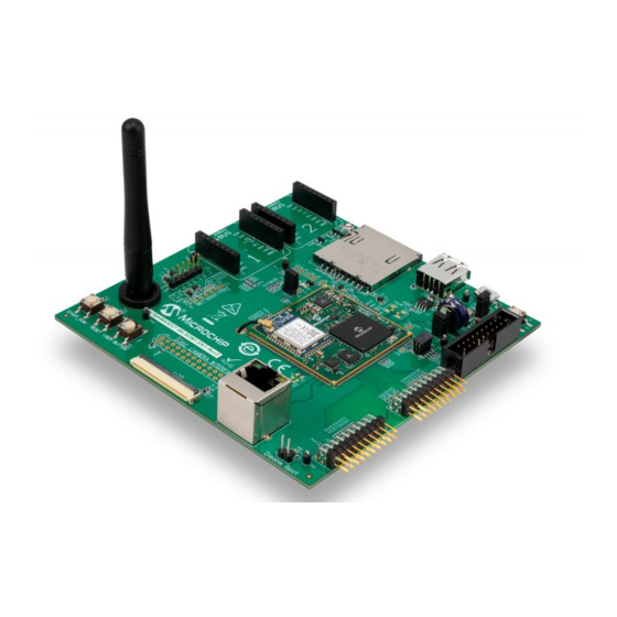
For the kit overview, see the figure below.
Figure 1. ATSAMA5D27-WLSOM1-EK1 Kit Overview
mikroBUS™ Click Interfaces
UART Debug Interfaces
Wi-Fi/BT Antenna
System & User Buttons
LCD & Camera Interfaces
©
2019 Microchip Technology Inc.
ATSAMA5D27-WLSOM1-EK1
10/100 Ethernet
Disable Boot
SD-CARD Interface
USB Host
Wi-Fi®/BT® Module
PTC Interface
User Guide
USB Device
WKUP Button
Backup Battery
JTAG Interface
SAMA5D27C-LD2G (SiP)
PTC Interface
DS50002931A-page 1
Advertisement
Table of Contents

Related Manuals for Microchip Technology ATSAMA5D27-WLSOM1-EK1


Summary of Contents for Microchip Technology ATSAMA5D27-WLSOM1-EK1
-
Page 1: Scope
ATSAMA5D27-WLSOM1-EK1 ATSAMA5D27-WLSOM1-EK1 User's Guide Scope This user's guide provides detailed information on the overall design of the ATSAMA5D27-WLSOM1-EK1 and describes how to use the kit. The kit is the evaluation platform for the SAMA5D27 System-In-Package (SiP) and SAMA5D27 Wireless System-On- Module (WLSOM1), and comprises: •... -
Page 2: Table Of Contents
Customer Change Notification Service......................58 Customer Support............................58 Product Identification System........................59 Microchip Devices Code Protection Feature....................59 Legal Notice..............................59 Trademarks..............................59 Quality Management System Certified by DNV................... 60 Worldwide Sales and Service........................61 User Guide DS50002931A-page 2 © 2019 Microchip Technology Inc. -
Page 3: Introduction
Table 1-1. Reference Data Sheets Document Title Available Document Ref. https://www.microchip.com/wwwproducts/en/ SAMA5D2 Series DS60001476 ATSAMA5D27 https://www.microchip.com/wwwproducts/en/ ATSAMA5D27-WLSOM1 DS60001590 ATSAMA5D27-WLSOM1 https://www.microchip.com/wwwproducts/en/ ATWILC3000-MR110UA DS70005327 ATWILC3000 SAMA5D2 System-In-Package (SiP) https://www.microchip.com/wwwproducts/en/ DS60001484 with LPDDR2 ATSAMA5D27C-LD2G User Guide DS50002931A-page 3 © 2019 Microchip Technology Inc. -
Page 4: Product Overview
One UART Interface 2x6 male connector One WILC UART Interface 2x6 male connector (Not populated) Board Monitor One RGB (Red, Green, Blue) LED – Four push button switches nSTART_SOM, Reset, Wakeup, User-free User Guide DS50002931A-page 4 © 2019 Microchip Technology Inc. -
Page 5: Kit Specification
The kit can only be supplied by USB Port Device (J10) interface. Table 2-3. Electrical Characteristics Electrical Parameter Value Maximum Input Voltage 5.5V Typical Input Voltage 5.0V Maximum Input Current I/O Voltage (on-board signals) 3.3V User Guide DS50002931A-page 5 © 2019 Microchip Technology Inc. -
Page 6: Baseboard Components
Baseboard Components Baseboard Components This section covers the specifications of the ATSAMA5D27-WLSOM1-EK1 and provides a high-level description of the baseboard's major components and interfaces. This document is not intended to provide a detailed documentation about the processor or about any other component used on the baseboard. It is expected that the user will refer to the appropriate documents of these devices to access detailed information. -
Page 7: Default Jumper Settings
ATSAMA5D27-WLSOM1-EK1 Baseboard Components Figure 3-2. ATSAMA5D27-WLSOM1-EK1 Block Diagram TAMPER 2 * mikroBUS User Buttons SYSTEM RBG LEDS MAIN 5.0V & SuperCap ATSAMA5D27-WLSOM1 JTAG & DBGU Interfaces DEBUG Disable Boot 2 * USB WILC DEBUG UART Default Jumper Settings The figure below shows the default jumper settings. Jumpers in red are configuration items and current measurement points. -
Page 8: Baseboard Connectors
Disable QSPI Boot Memory Closed VDD_MAIN WLSOM1 Current Measurement Closed VDDBU WLSOM1 Current Measurement Baseboard Connectors The following table describes the interface connectors on the ATSAMA5D27-WLSOM1-EK1. Table 3-2. Baseboard Interface Connectors Connector Interfaces to SHDN Signal Supervising (Not populated) VDD_3V3 WLSOM1 Current Measurement... -
Page 9: Function Blocks
64 Mb Serial Quad I/O Flash Memory (SST26VF064BEUIT-104I/MF) with Embedded EUI-48 and EUI-64 MAC Addresses ® • IEEE 802.11 b/g/n Wi-Fi plus Bluetooth (Wi-Fi/BT) Module (ATWILC3000-MR110UA) • 10Base-T/100Base-TX Ethernet PHY (KSZ8081RNAIA) • ATECC608A Secure Element User Guide DS50002931A-page 9 © 2019 Microchip Technology Inc. - Page 10 3.4.2.1 Input Power The ATSAMA5D27-WLSOM1-EK1 power source can come through a USB connector (J10) connected to a PC. This USB power source is sufficient to supply the board in most applications. Important: In case of an external device connected through the USB-B port, it is recommended to use the 5V power supply input with an AC/DC wall adapter for the entire system rather than a PC or a USB hub, which are limited to 500 mA typical.
- Page 11 3.4.2.4 Backup Power Supply The ATSAMA5D27-WLSOM1-EK1 features a power source in order to permanently power the backup area of the SAMA5D2 device (refer to the SAMA5D2 Series datasheet). A super capacitor (C13) sustains such permanent power to VDDBU when all system power sources are off.
- Page 12 3.4.5.1 Secure Digital Multimedia Card (SDMMC) Controller The ATSAMA5D27-WLSOM1-EK1 features two Secure Digital Multimedia Card (SDMMC) interfaces that support the MultiMedia Card (e.MMC) Specification V4.41, the SD Memory Card Specification V3.0, and the SDIO V3.0 specification. It is compliant with the SD Host Controller Standard V3.0 Specification.
- Page 13 0402 1% R158 SDMMC0_DAT2_PA04 DAT2 0402 1% R159 SDMMC0_CD_PA13 SHIELD SDMMC0_WP_PA12 Figure 3-10. VDDSDHC Power Switch Schematic VDD_1V8 VDD_3V3 VDDSDHC ADG849 SDMMC0_VDDSEL_PA11 VDD_3V3 0402 0.1uF 0402 IN=0: S1 Closed IN=1: S2 Closed 0402 User Guide DS50002931A-page 13 © 2019 Microchip Technology Inc.
- Page 14 Signal Description DAT3 Data Line Command/Response Line VSS1 – GROUND VDDSDHC – Power Line (3.3V/1.8V) Clock Line VSS2 – GROUND DAT0 Data Line DAT1 Data Line DAT2 Data Line PA13 Card Detect User Guide DS50002931A-page 14 © 2019 Microchip Technology Inc.
- Page 15 ETH_TX_P DIFF100 ETH_TX_N DIFF100 ETH_RX_P DIFF100 ETH_RX_N 0.1uF 0.1uF 0402 0402 Green 120R Right GND_ETH 0402 Yellow BLM18PG121SN1D VDD_3V3 470R 0402 Lift EARTH_ETH GND_ETH ETH_LED0 CON RJ-45 JD2-0010NL JD2-0010NL EARTH_ETH EARTH_ETH User Guide DS50002931A-page 15 © 2019 Microchip Technology Inc.
- Page 16 Receive differential pair decoupling capacitor Receive negative differential pair EARTH GROUND Yellow LED anode. Connected to ETH_LED0 Yellow LED cathode. Connected to VDD_3V3 through 470R resistor. Green LED anode (Not connected) User Guide DS50002931A-page 16 © 2019 Microchip Technology Inc.
- Page 17 – Offers a VBUS detection function through the R81-R83 resistor ladder – Used as a secondary power source and as a communication link for the ATSAMA5D27-WLSOM1-EK1, and derives power from the PC over the USB cable. In most cases, this port is limited to 500 mA.
- Page 18 GROUND – USB_DETECT PA16 VBUS Insertion Detection 3.4.6.4 USB-B Interface and Power Switch The figure below shows the USB implementation on the USB-B port terminated on USB Type A connector J11. User Guide DS50002931A-page 18 © 2019 Microchip Technology Inc.
- Page 19 90Ω ±10% differential trace impedance 0603 0402 USB2.0 STD-A FEMALE Routing top or bottom 120R BLM18PG121SN1D EARTH_USB_B Figure 3-17. USB-B Host Connector J11 Location The table below describes the pin assignment of USB-B connector J11. User Guide DS50002931A-page 19 © 2019 Microchip Technology Inc.
- Page 20 The HSIC port is connected to 2 U.FL connectors (not populated by default). Figure 3-18. HSIC Interface Schematic HSIC Matched Net Lengths [Tolerance = 0.25mm] STROBE U.FL RF Coaxial U.FL Male 50Ω ± 10% single-ended trace impedance DATA U.FL RF Coaxial U.FL Male User Guide DS50002931A-page 20 © 2019 Microchip Technology Inc.
-
Page 21: External Interfaces
External Interfaces 3.5.1 LCD TFT Interface The ATSAMA5D27-WLSOM1-EK1 provides an FPC connector with 18 bits of data and control signals to the LCD interface. This connector is used to connect to an LCD display type AC320005-5. A 50-pin FPC (J21) header is provided on the baseboard to interface the LCD module with the 18-bit parallel RGB mode and is used to connect to an LCD display type AC320005-5. -
Page 22: Lcd Interface
NRST R107 0R 0402 SPI1 Signals Distribution VDD_3V3 VDD_MAIN PC01 0402 1% SPI1_SPCK_LCD_PC01 FFC/FPC 50P Female 0402 1% PC03 0.1uF SPI1_MISO_LCD_PC03 PC02 0402 1% 0402 0402 SPI1_MOSI_LCD_PC02 PC06 0402 1% SPI1_NPCS2_LCD_PC06 User Guide DS50002931A-page 22 © 2019 Microchip Technology Inc. - Page 23 Data Line (BLUE 2) LCDDAT3 PC11 Data Line (BLUE 3) – – Ground LCDDAT4 PC12 Data Line (BLUE 4) LCDDAT5 PC13 Data Line (BLUE 5) LCDDAT6 PC14 Data Line (BLUE 6) User Guide DS50002931A-page 23 © 2019 Microchip Technology Inc.
- Page 24 ENABLE Display Enable Signal PD19 TWI_DATA I²C Data Line (maXTouch) TWCK PD20 TWI_CLOCK I²C clock Line (maXTouch) GPIO IRQ1 maXTouch Interrupt Line GPIO PA17 IRQ2 Interrupt Line for other I²C devices User Guide DS50002931A-page 24 © 2019 Microchip Technology Inc.
- Page 25 0402 1% ISC_PCK_PC21 PC22 0402 1% ISC_VSYNC_PC22 PC23 0402 1% ISC_HSYNC_PC23 0402 1% PC24 ISC_MCK_PC24 C Signals Distribution VDD_3V3 2.2k 2.2k 0402 0402 0402 1% PD19 TWD1_ISC_PD19 0402 1% PD20 TWCK1_ISC_PD20 User Guide DS50002931A-page 25 © 2019 Microchip Technology Inc.
- Page 26 ISC_MCK PC24 Master Clock GROUND – ISC_VSYNC PC22 Vertical Synchro GROUND – ISC_HSYNC PC23 Horizontal Synchro GROUND – ISC_PCK PC21 Clock GROUND – ISC_D0 Data0 Data1 PC10 ISC_D1 ISC_D2 PC11 Data2 User Guide DS50002931A-page 26 © 2019 Microchip Technology Inc.
- Page 27 – GROUND 3.5.3 RGB LED The ATSAMA5D27-WLSOM1-EK1 features one RGB LED which can be controlled by the user. The three LED cathodes are controlled via GPIOs or Timer/Counter pins (only for red and green LEDs). Figure 3-24. RGB LED Schematic VDD_3V3 2.2k...
-
Page 28: Debugging Capabilities
GREEN_LED GPIO/TIOB5 BLUE_LED GPIO Debugging Capabilities The ATSAMA5D27-WLSOM1-EK1 includes two main debugging interfaces to provide debug-level access to the SAMA5D2: • One JTAG interface connected from the MPU using connector J25. • One UART interface connected from the MPU using connector J26. - Page 29 100k 100k 0402 0402 0402 JTAG_TDI_PD28 JTAG_TMS_PD30 JTAG_TCK_PD27 JTAG_TDO_PD29 R125 100R NRST HDR-2.54 Male 2x10 Figure 3-27. JTAG Connector J25 Location The table below describes the pin assignment of JTAG connector J25. User Guide DS50002931A-page 29 © 2019 Microchip Technology Inc.
- Page 30 3.6.2 Debug UART The ATSAMA5D27-WLSOM1-EK1 board has a dedicated serial port for debugging, which is accessible through the 6-pin male header J26. Various interfaces can be used as a USB/Serial DBGU port bridge, such as FTDI TTL-232R USB to TTL serial cable or basic breakout board for the RS232/USB converter.
- Page 31 R152 and R154 are optional (not implemented) resistors that can be used for power selection. Power can be delivered either by the ATSAMA5D27-WLSOM1-EK1 board or by the debug interface tool. To avoid malfunction between the debug interface (e.g., FTDI) and the on-board power system, ensure that the voltage level selected corresponds to the application requirements.
- Page 32 Handshake Output – GROUND 3.6.3 WILC3000 Debug UART The ATSAMA5D27-WLSOM1-EK1 has a dedicated serial port for WILC3000 Module debugging, which is accessible through the 6-pin male header J27 (not populated by default). User Guide DS50002931A-page 32 © 2019 Microchip Technology Inc.
- Page 33 DBGU_TXD DBGU_TX_PB27 R144 R146 R148 R150 R152 R154 NL17SZ126-D 0402 0402 0402 0402 0402 0402 DBGU_CTS DBGU_TXD DBGU_RXD VDD_3V3 DBGU_RTS R171 HDR-2.54 Male 1x6 100k 0402 0.1uF 0402 DBGU_RX_PB26 DBGU_RXD NL17SZ126-D User Guide DS50002931A-page 33 © 2019 Microchip Technology Inc.
-
Page 34: Pio Usage On Expansion Connectors
RS232 serial data input signal – 3.3V or 5V Supply WILCFTDI_RTS Handshake Output – GROUND PIO Usage on Expansion Connectors This section describes the signals and connectors related to the PIO usage on expansion connectors. User Guide DS50002931A-page 34 © 2019 Microchip Technology Inc. - Page 35 Note that most pins are configured as GPIO inputs, with a 100 KOhm pull-up resistor, after reset. 3.7.1 Tamper Interface The ATSAMA5D27-WLSOM1-EK1 features seven tamper pins for static or dynamic intrusion detection and two analog pins for comparison. For a description of intrusion detection, refer to the SAMA5D2 data sheet, chapter “Security Module (SECUMOD)”.
- Page 36 3.7.2 mikroBUS Interfaces The ATSAMA5D27-WLSOM1-EK1 hosts two pairs of 8-pin female headers acting as mikroBUS interfaces. The mikroBUS standard defines the main board sockets and add-on boards, or Click boards, used for interfacing microprocessors with integrated modules having proprietary pin configuration and silkscreen markings. The pinout consists of three groups of communication pins (SPI, UART and TWI), four additional pins (PWM, interrupt, analog input and reset) and two power groups (+3.3V and GND on the left, and 5V and GND on the right 1x8 header).
- Page 37 UART Receive SPI Clock mikroBUS1_SCK UTXD PB11 UART Transmit SPI MISO mikroBUS1_MISO TWCK PD20 TWI Clock SPI MOSI mikroBUS1_MOSI PD19 TWI Data 3.3V – VDD_3V3 VDD_MAIN – GROUND – – GROUND User Guide DS50002931A-page 37 © 2019 Microchip Technology Inc.
- Page 38 Figure 3-37. mikroBUS2 Connector J20 Location The table below describes the pin assignment of mikroBUS2 connector J20. Table 3-15. mikroBUS2 Connectors Pin Assignment Function Signal Pin No Signal Function Analog Input PD26 mikroBUS2_AN mikroBUS2_PWM PA31 User Guide DS50002931A-page 38 © 2019 Microchip Technology Inc.
- Page 39 GROUND 3.7.3 Expansion Header Interfaces The ATSAMA5D27-WLSOM1-EK1 can host two connectors to interface with standard Xplained Pro extensions and, in particular, with QT Xplained Pro Extension boards. The following QT Xplained Pro Extensions boards are compatible with the interfaces: •...
- Page 40 PTC_COL4_PD115 PTC_COL5_PD16 PD16 PTC COL TWI Data PD19 TWD1_XPRO_PD19 TWCK1_XPRO_PD20 PD20 TWI Clock – – PTC LED PA14 XPRO_LED_2_PA14 PTC_COL6_PD17 PD17 PTC COL PTC COL PD17 PTC_COL0_PD11 PTC_COL7_PD18 PD18 PTC COL User Guide DS50002931A-page 40 © 2019 Microchip Technology Inc.
-
Page 41: Extra Features
A 2-pin connector (J14), not populated by default, is available on the baseboard to measure output current capability of the VLDO2 regulator. Note: The maximum current available on VLDO2 node is approximately 300 mA max @ 1.2V to 3.3V. User Guide DS50002931A-page 41 © 2019 Microchip Technology Inc. - Page 42 VTH Threshold The ATSAMA5D27-WLSOM1 module mounted on the base board integrates a Voltage Supervisor MIC842. A resistor ladder is mounted on the ATSAMA5D27-WLSOM1-EK1 board and detects a voltage drop when reduced to 4.64V. It is possible to change this resistor ladder, values or reference if, for test purposes, another voltage reference is monitored (e.g.
- Page 43 ATSAMA5D27-WLSOM1-EK1 Baseboard Components Figure 3-42. VTH Threshold Schematic VDD_MAIN 787k 0402 Threshold = 4.64V 287K 0402 User Guide DS50002931A-page 43 © 2019 Microchip Technology Inc.
-
Page 44: Installation And Operation
ATSAMA5D27-WLSOM1-EK1 Installation and Operation Installation and Operation System and Configuration Requirements The ATSAMA5D27-WLSOM1-EK1 requires the following: • Personal Computer • USB cable (included in the kit box) • Wireless antenna (included in the kit box) How to Mount the Wireless Antenna on the Kit 4.2.1... - Page 45 Figure 4-6. Reorganize the antenna cable 4.2.4 Antenna Orientation The antenna has 180° free orientation for ease-of-use. Nonetheless, a 90° rotation is sufficient as shown below, when mikroBUS clicks and button are used. User Guide DS50002931A-page 45 © 2019 Microchip Technology Inc.
-
Page 46: Baseboard Setup
Connect the other end of the cable to a free port of your PC. Open a terminal (console 115200, N, 8, 1) on your personal computer. Reset the baseboard. A start-up message appears on the console. User Guide DS50002931A-page 46 © 2019 Microchip Technology Inc. -
Page 47: Appendix: Schematics And Layouts
Figure 5-1. ATSAMA5D27-WLSOM1-EK1 Schematic: Page 1 rotatethispage90 BASEBOARD CONNECTIONS + WLSOM INTERNAL CONNECTIONS PIOA USAGE PIOA USAGE PIOB USAGE PIOB USAGE PIOC USAGE PIOC USAGE PIOD USAGE PIOD USAGE LCD_PCLK SDMMC0_CK PA16 USB_DETECT XPRO_LED_8 PB16 ETH_GRXDV RST_mBUS2 PC16 LCD_D10 PD16 PTC_COL5... - Page 48 Figure 5-2. ATSAMA5D27-WLSOM1-EK1 Schematic: Page 2 rotatethispage90 SAMA5D2-WLSOM1 VDD_MAIN VDDFUSE PA00 SDMMC0_CLK_PA00 PB00 XPRO_LED_8_PB00 PC00 PD00 VDD_MAIN VDDFUSE RST_mBUS2_PC00 0402 1% PC01 R164 VLDO2 PA01 SDMMC0_CMD_PA01 PB01 XPRO_LED_17_PB01 PC01 PD01 LCD_DATA_EN_PD01 VDD_MAIN PC02 PA02 SDMMC0_DAT0_PA02 PB02 USER_BUTTON_PB02 PC02 PD02 INT_mBUS1_PD02 VDD_MAIN...
- Page 49 Figure 5-3. ATSAMA5D27-WLSOM1-EK1 Schematic: Page 3 rotatethispage90 POWER USB INTERFACE VBUS_USBA VDD_MAIN VDD_MAIN VDDBU VBUS_USBA 120R VOUT 100k 100R HDR-2.54 Male 1x2 USB_DETECT_PA16 USBA 0402 0402 HDR-2.54 Male 1x2 BLM18PG121SN1D 0.1uF BAT54C 20pF RB160M-60TR SHDN 0.1uF 200k 100uF 22uF 0.1uF 0.1uF...
- Page 50 Figure 5-4. ATSAMA5D27-WLSOM1-EK1 Schematic: Page 4 rotatethispage90 SD/MMC INTERFACE ETHERNET VDDSDHC VDD_3V3 0.1uF 10000pF 4.7uF 100Ω ±5Ω differential trace impedance Routing top or bottom SDMMC 0402 0402 0402 0402 0402 0402 0402 0402 0402 0402 DIFF100 Matched Net Lengths [Tolerance = 0.25mm]...
- Page 51 Figure 5-5. ATSAMA5D27-WLSOM1-EK1 Schematic: Page 5 rotatethispage90 ISC CAMERA INTERFACE VDD_3V3 BLM18PG121SN1D 120R 0402 1% R102 0402 1% ISC_NRST_PA09 ISC_PWD_XPRO_LED_15_PC07 LCD INTERFACE TWCK1_ISC_PD20 TWD1_ISC_PD19 ISC_MCK_PC24 ISC_VSYNC_PC22 ISC_HSYNC_PC23 ISC_PCK_PC21 ISC_D0_PC09 ISC_D1_PC10 ISC_D2_PC11 ISC_D3_PC12 ISC_D4_PC13 LCD_ID_PC09 ISC_D5_PC14 ISC_D6_PC15 ISC_D7_PC16 ISC_D8_PC17 Matched Net Lengths [Tolerance = 1.27mm]...
- Page 52 Figure 5-6. ATSAMA5D27-WLSOM1-EK1 Schematic: Page 6 rotatethispage90 XPRO INTERFACE DEBUG FTDI VDD_3V3 0.1uF 0402 XPRO EXT1 VDD_3V3 VDD_MAIN DBGU_TXD R113 R132 DBGU_TX_PB27 PTC_COL0_PD11 PTC_COL1_PD12 R114 R133 PTC_COL2_PD13 PTC_COL3_PD14 R115 R134 R144 R146 R148 R150 R152 R154 100R 100R NL17SZ126-D XPRO_LED_7_PB30 XPRO_LED_17_PB01...
- Page 53 ATSAMA5D27-WLSOM1-EK1 Appendix: Schematics and Layouts Figure 5-7. ATSAMA5D27-WLSOM1-EK1 Layout: Top Layer Figure 5-8. ATSAMA5D27-WLSOM1-EK1 Layout: Inner Layer 2 - Ground User Guide DS50002931A-page 53 © 2019 Microchip Technology Inc.
- Page 54 ATSAMA5D27-WLSOM1-EK1 Appendix: Schematics and Layouts Figure 5-9. ATSAMA5D27-WLSOM1-EK1 Layout: Inner Layer 3 - Signals Figure 5-10. ATSAMA5D27-WLSOM1-EK1 Layout: Inner Layer 4: Signals User Guide DS50002931A-page 54 © 2019 Microchip Technology Inc.
- Page 55 ATSAMA5D27-WLSOM1-EK1 Appendix: Schematics and Layouts Figure 5-11. ATSAMA5D27-WLSOM1-EK1 Layout: Inner Layer 5: Power Figure 5-12. ATSAMA5D27-WLSOM1-EK1 Layout: Bottom Layer User Guide DS50002931A-page 55 © 2019 Microchip Technology Inc.
-
Page 56: Ordering Information
Ordering Information Table 6-1. Ordering Details Ordering Code Dimensions Description Regulatory Information ATSAMA5D27-WLSOM1-EK1 Certified MPU Wireless Module with SAMA5D27, 120 x 120 mm FCC, IC, CE, RED (DM320117) WILC3000 and U.FL connector User Guide DS50002931A-page 56 © 2019 Microchip Technology Inc. -
Page 57: Revision History
ATSAMA5D27-WLSOM1-EK1 Revision History Revision History Rev. A - 10/2019 First issue. User Guide DS50002931A-page 57 © 2019 Microchip Technology Inc. -
Page 58: The Microchip Web Site
A listing of sales offices and locations is included in the back of this document. Technical support is available through the web site at: http://www.microchip.com/support User Guide DS50002931A-page 58 © 2019 Microchip Technology Inc. -
Page 59: Product Identification System
HyperLight Load, IntelliMOS, Libero, motorBench, mTouch, Powermite 3, Precision Edge, ProASIC, ProASIC Plus, ProASIC Plus logo, Quiet-Wire, SmartFusion, SyncWorld, Temux, TimeCesium, TimeHub, TimePictra, TimeProvider, Vite, WinPath, and ZL are registered trademarks of Microchip Technology Incorporated in the U.S.A. Adjacent Key Suppression, AKS, Analog-for-the-Digital Age, Any Capacitor, AnyIn, AnyOut, BlueSky, BodyCom, CodeGuard, CryptoAuthentication, CryptoAutomotive, CryptoCompanion, CryptoController, dsPICDEM, dsPICDEM.net, Dynamic Average Matching, DAM, ECAN, EtherGREEN, In-Circuit Serial Programming, ICSP,... -
Page 60: Quality Management System Certified By Dnv
The Adaptec logo, Frequency on Demand, Silicon Storage Technology, and Symmcom are registered trademarks of Microchip Technology Inc. in other countries. GestIC is a registered trademark of Microchip Technology Germany II GmbH & Co. KG, a subsidiary of Microchip Technology Inc., in other countries. -
Page 61: Worldwide Sales And Service
New York, NY Sweden - Stockholm Tel: 631-435-6000 Tel: 46-8-5090-4654 San Jose, CA UK - Wokingham Tel: 408-735-9110 Tel: 44-118-921-5800 Tel: 408-436-4270 Fax: 44-118-921-5820 Canada - Toronto Tel: 905-695-1980 Fax: 905-695-2078 User Guide DS50002931A-page 61 © 2019 Microchip Technology Inc.
Need help?
Do you have a question about the ATSAMA5D27-WLSOM1-EK1 and is the answer not in the manual?
Questions and answers