
Related Manuals for Aaeon ETX-945GSE


Summary of Contents for Aaeon ETX-945GSE
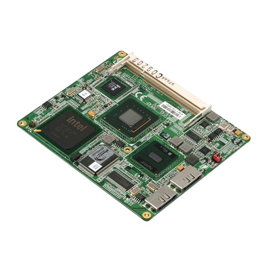
- Page 1 E T X C P U M o d u l e E T X - 9 4 5 G S E ETX-945GSE ® Onboard Intel Atom N270 Processor Non-ECC DDRII 400/533 Memory With LCD, Ethernet, PCI, ISA, Audio, SATA, SDVO ETX-945GSE Manual Rev. A 3rd Ed. Sept. 2010...
- Page 2 AAEON assumes no liabilities resulting from errors or omissions in this document, or from the use of the information contained herein. AAEON reserves the right to make changes in the product design without notice to its users.
- Page 3 E T X C P U M o d u l e E T X - 9 4 5 G S E Acknowledgments All other products’ name or trademarks are properties of their respective owners. Award is a trademark of Award Software International, Inc. ®...
- Page 4 Before you begin installing your card, please make sure that the following materials have been shipped: • 1 ETX-945GSE CPU Module • 1 CD-ROM for manual (in PDF format) and drivers If any of these items should be missing or damaged, please...
- Page 5 E T X C P U M o d u l e E T X - 9 4 5 G S E Application Notes ® After installing drivers in AT power mode under Windows operation, there is no message: “It is now safe to turn off your computer”...
-
Page 6: Table Of Contents
E T X C P U M o d u l e E T X - 9 4 5 G S E Contents Chapter 1 General Information 1.1 Introduction..............1-2 1.2 Features ..............1-3 1.3 Specifications ............1-4 Chapter 2 Quick Installation Guide 2.1 Safety Precautions ............ - Page 7 E T X C P U M o d u l e E T X - 9 4 5 G S E Appendix A Programming The Watchdog Timer A.1 Programming ............A-2 A.2 W83627HG Watchdog Timer Initial Program ..A-6 Appendix B I/O Information B.1 I/O Address Map ............B-2 B.2 1 MB Memory Address Map ........B-3...
-
Page 8: Chapter 1 General Information
E T X C P U M o d u l e E T X - 9 4 5 G S E Chapter General Information 1 - 1 Chapter 1 General Information... -
Page 9: Introduction
For the display specifications, ETX-945GSE integrates Intel 945GSE and shared system memory is up to 224MB/DVMT 3.0. The display of ETX-945GSE supports CRT and 18/24-bit dual-channel LVDS LCD. Moreover, it supports NTSC/ PAL and Composite Video, S-Video on the carrier board. In addition, one SDVO port can be used through the SDVO connector to provide more flexibility for display function. -
Page 10: Features
E T X C P U M o d u l e E T X - 9 4 5 G S E 1.2 Features ® Onboard Intel Atom™ N270 Processor ® Intel 945GSE + ICH7M DDRII 400/533 Memory, Max. 1GB 10/100Base-TX Ethernet CRT, Up to 24-bit Dual-channel LVDS LCD, TV, SDVO Connector x 1... -
Page 11: Specifications
E T X C P U M o d u l e E T X - 9 4 5 G S E 1.3 Specifications System ® Onboard Intel Atom™ N270 Processor 1.6GHz, FSB 533MHz Memory One 200-pin DDR II SODIMM, supports DDR II 400/533 up to 1GB, non ECC function only ®... - Page 12 Shared system memory up to 224MB/ DVMT 3.0 Resolution Up to 2048x1536 (QXGA) for CRT; Up to 1600x1200 (UXGA) for LCD LCD Interface 18-bit dual-channel LVDS (TF-ETX-945GSE-A10); 24-bit dual-channel LVDS (TF-ETX-945GSE-A10-01) SDVO Port SDVO port x 1 TV-Out Intel 945GSE integrated, supports NTSC/PAL;...
- Page 13 E T X C P U M o d u l e E T X - 9 4 5 G S E Floppy Disk Drive x 1 Serial Port Parallel Port USB2.0 x 4 GPIO PS/2 Port Keyboard x 1, Mouse x 1 IrDA One IrDA Tx/Rx header Audio...
-
Page 14: Chapter 2 Quick Installation Guide
E T X C P U M o d u l e E T X - 9 4 5 G S E Chapter Quick Installation Guide Chapter 2 Quick Installation Guide... -
Page 15: Safety Precautions
E T X C P U M o d u l e E T X - 9 4 5 G S E 2.1 Safety Precautions Always completely disconnect the power cord from your board whenever you are working on it. Do not make connections while the power is on, because a sudden rush of power can damage sensitive electronic components. -
Page 16: Mechanical Drawing
E T X C P U M o d u l e E T X - 9 4 5 G S E 2.2 Mechanical Drawing Component Side Solder Side Chapter 2 Quick Installation Guide... -
Page 17: List Of Jumpers
E T X C P U M o d u l e E T X - 9 4 5 G S E 2.3 List of Jumpers The board has a number of jumpers that allow you to configure your system to suit your application. The table below shows the function of each of the board's jumpers: Jumpers Function... -
Page 18: At/Atx & Back Light Selection (Jp1)
E T X C P U M o d u l e E T X - 9 4 5 G S E 2.5 AT/ATX & Back Light Selection (JP1) Function AT mode ATX mode (Default) Back light high enable (Default) Back light low enable 2.6 SDVO Extension Slot (CN2) Signal... -
Page 19: Etx Connector (X1A)
E T X C P U M o d u l e E T X - 9 4 5 G S E 2.7 SPI Flash Programming Connector (Optional) (CN3) Signal Signal +3.3V SPI_CS#0 SPI_CLK SPI_SO SPI_SI 2.8 ETX Connector (X1A) Signal Signal Signal... -
Page 20: Etx Connector (X1B)
E T X C P U M o d u l e E T X - 9 4 5 G S E AD11 MIC_IN AD27 AD29 AD12 LIN_R AD30 USB1P AD13 VCCAUD PCIRST# AD31 AD14 LOUT_L INTC# INTD# AD15 GNDAUD INTA# INTB# CBE1#... -
Page 21: Etx Connector (X1C)
E T X C P U M o d u l e E T X - 9 4 5 G S E NOWS# BALE DREQ2 IRQ9 DACK2# IRQ3 IOCHK# RSTDRV IRQ4 2.10 ETX Connector (X1C) Parallel Port Mode Pinout Signal Signal Signal Signal... - Page 22 E T X C P U M o d u l e E T X - 9 4 5 G S E TXOUT00 TXOUT01 RTS1# BUSY# TXOUT00# TXOUT01# DTR1# DCD1# SLCT# LVDS_ DVOCVSY DSR1# MSCLK DDCPDATA LVDS_ LVDS_BK CCTS1# MSDAT DDCPCLK LVDS_ LVDS_DIG...
-
Page 23: Etx Connector (X1D)
E T X C P U M o d u l e E T X - 9 4 5 G S E RXD1 DRV# TXOUT00 TXOUT01 RTS1# MOT# TXOUT00# TXOUT01# DTR1# WDATA# DCD1# WGATE# LVDS_ DVOCVSY DSR1# MSCLK DDCPDATA LVDS_ LVDS_BKL CCTS1# MSDAT... - Page 24 E T X C P U M o d u l e E T X - 9 4 5 G S E PIDE_CS3# PIDE_D10 PIDE_CS1# PIDE_D5 PIDE_A2 PIDE_D9 PIDE_A0 PIDE_D6 PIDE_A1 RING# P66DET S66DET/ RXD# PIDE_D8 PIDE_INTR PIDE_ACK TXD# PIDE_D7 PIDE_RDY HDRST# 2-11...
- Page 25 E T X C P U M o d u l e E T X - 9 4 5 G S E Below Table for China RoHS Requirements 产品中有毒有害物质或元素名称及含量 AAEON Main Board/ Daughter Board/ Backplane 有毒有害物质或元素 部件名称 铅 汞 镉...
-
Page 26: Chapter 3 Award Bios Setup
E T X C P U M o d u l e E T X - 9 4 5 G S E Chapter Award BIOS Setup Chapter 3 Award BIOS Setup... - Page 27 You have changed the hardware attached to your system The CMOS memory has lost power and the configuration information has been erased. The ETX-945GSE memory has an integral lithium battery backup for data retention. However, you will need to replace the complete unit when it finally runs down.
- Page 28 E T X C P U M o d u l e E T X - 9 4 5 G S E 3.2 Award BIOS Setup Awards BIOS ROM has a built-in Setup program that allows users to modify the basic system configuration. This type of information is stored in battery-backed CMOS RAM so that it retains the Setup information when the power is turned off.
- Page 29 Save CMOS value changes to CMOS and exit setup. Exit Without Saving Abandon all CMOS value changes and exit setup. For more detailed information, you can refer to the "AAEON BIOS Item Description.pdf" file in the CD for the meaning of each setting in this chapter.
-
Page 30: Chapter 4 Driver Installation
E T X C P U M o d u l e E T X - 9 4 5 G S E Chapter Driver Installation Chapter 4 Driver Installation... - Page 31 E T X C P U M o d u l e E T X - 9 4 5 G S E The ETX-945GSE comes with a CD-ROM that contains all drivers and utilities that meet your needs. Follow the sequence below to install the drivers: Step 1 –...
- Page 32 E T X C P U M o d u l e E T X - 9 4 5 G S E 4.1 Installation: Insert the ETX-945GSE CD-ROM into the CD-ROM Drive. And install the drivers from Step 1 to Step 5 in order. Step 1 – Install INF Driver 1.
- Page 33 E T X C P U M o d u l e E T X - 9 4 5 G S E OS your system is 2. Double click on the .exe file located in each OS folder 3. Follow the instructions that the window shows 4.
-
Page 34: Appendix A Programming The Watchdog Timer
E T X C P U M o d u l e E T X - 9 4 5 G S E Appendix Programming the Watchdog Timer Appendix A Programming the Watchdog Timer... -
Page 35: Programming
ETX-945GSE utilizes W83627HG chipset as its watchdog timer controller. Below are the procedures to complete its configuration and the AAEON intial watchdog timer program is also attached based on which you can develop customized program to fit your application. Configuring Sequence Description... - Page 36 E T X C P U M o d u l e E T X - 9 4 5 G S E (3) Exit the W83627HG config Mode. Undesired result may occur if the config Mode is not exited normally. (1) Enter the W83627HG config Mode To enter the W83627HG config Mode, two special I/O write operations are to be performed during Wait for Key state.
- Page 37 E T X C P U M o d u l e E T X - 9 4 5 G S E = 10 Power LED pin is a 1Hz toggle pulse with 50 duty cycle. = 11 Power LED pin is a 1/4Hz toggle pulse with 50 duty cycle.
- Page 38 E T X C P U M o d u l e E T X - 9 4 5 G S E WatchDog Timer Register III (Index=F7h, Default=00h) Bit 7 : Mouse interrupt reset Enable or Disable Watchdog Timer is reset upon a Mouse interrupt Watchdog Timer is not affected by Mouse interrupt...
-
Page 39: W83627Hg Watchdog Timer Initial Program
E T X C P U M o d u l e E T X - 9 4 5 G S E A.2 W83627HG Watchdog Timer Initial Program Example: Setting 10 sec. as Watchdog timeout interval ;/////////////////////////////////////////////////////////////////////////////////////////////// Mov dx,2eh ;Enter W83627HG config mode Mov al,87h (out 87h to 2eh twice) Out dx,al... - Page 40 E T X C P U M o d u l e E T X - 9 4 5 G S E ;/////////////////////////////////////////////////////////////////////////////////////////////// Dec dx Mov al,0f5h ;CRF5 (PLED mode register) Out dx,al Inc dx In al,dx And al,not 08h ;Set second as counting unit Out dx,al ;///////////////////////////////////////////////////////////////////////////////////////////////...
-
Page 41: Appendix B I/O Information
E T X C P U M o d u l e E T X - 9 4 5 G S E Appendix I/O Information B - 1 Appendix B I/O Information... -
Page 42: I/O Address Map
E T X C P U M o d u l e E T X - 9 4 5 G S E B.1 I/O Address Map B - 2 Appendix B I/O Information... -
Page 43: St Mb Memory Address Map
E T X C P U M o d u l e E T X - 9 4 5 G S E B.2 1 MB Memory Address Map B - 3 Appendix B I/O Information... -
Page 44: Irq Mapping Chart
E T X C P U M o d u l e E T X - 9 4 5 G S E B.3 IRQ Mapping Chart B.4 DMA Channel Assignments B - 4 Appendix B I/O Information...
Need help?
Do you have a question about the ETX-945GSE and is the answer not in the manual?
Questions and answers