Table of Contents
Advertisement
Quick Links
Advertisement
Table of Contents

Related Manuals for Aaeon GENE-QM57


Summary of Contents for Aaeon GENE-QM57
- Page 1 G E N E - Q M 5 7 GENE-QM57 ® ® Intel Core™i7/i5 Mobile/Celeron Processor ® Intel QM57/HM55 10/100/1000Base-TX 2 SATA 3.0Gb/s, CompactFlash™ 2 COM, 8 USB2.0, Digital I/O 1 Mini Card GENE-QM57 Manual Rev.A 3rd Ed. July 2013...
- Page 2 AAEON assumes no liabilities resulting from errors or omissions in this document, or from the use of the information contained herein. AAEON reserves the right to make changes in the product design without notice to its users.
- Page 3 S u b C o m p a c t B o a r d G E N E - Q M 5 7 Acknowledgments All other products’ name or trademarks are properties of their respective owners. AMI is a trademark of American Megatrends Inc. ...
- Page 4 Before you begin installing your card, please make sure that the following materials have been shipped: DVD-ROM for manual (in PDF format) and drivers GENE-QM57 If any of these items should be missing or damaged, please contact your distributor or sales representative immediately.
-
Page 5: Table Of Contents
S u b C o m p a c t B o a r d G E N E - Q M 5 7 Contents Chapter 1 General Information 1.1 Introduction..............1-2 1.2 Features ..............1-3 1.3 Specifications ............1-4 Chapter 2 Quick Installation Guide 2.1 Safety Precautions ............ - Page 6 S u b C o m p a c t B o a r d G E N E - Q M 5 7 2.16 LVDS (1)- Inverter +5V/+12V Connector (CN6)..2-13 2.17 LVDS (1) LCD Connector (CN7) ......2-13 2.18 LPT Connector (CN10) (Optional)......
- Page 7 S u b C o m p a c t B o a r d G E N E - Q M 5 7 Chapter 4 Driver Installation 4.1 Installation ..............4-3 Appendix A Programming The Watchdog Timer A.1 Programming ............A-2 A.2 ITE8712 Watchdog Timer Initial Program....A-6 Appendix B I/O Information B.1 I/O Address Map ............B-2...
-
Page 8: Chapter 1 General Information
S u b C o m p a c t B o a r d G E N E - Q M 5 7 Chapter General Information 1- 1 Chapter 1 General Information... -
Page 9: Introduction
S u b C o m p a c t B o a r d G E N E - Q M 5 7 1.1 Introduction AAEON, a leading embedded boards manufacturer, is pleased to announce the debut of their new generation 3.5” SubCompact Board—GENE-QM57. The GENE-QM57 is a cutting-edge product that provides high performance and low power consumption in the embedded market. -
Page 10: Features
S u b C o m p a c t B o a r d G E N E - Q M 5 7 1.2 Features ® ® Intel Core™ i7/i5 Mobile/ Celeron (32nm) Processor ® Intel QM57/HM55 ... -
Page 11: Specifications
S u b C o m p a c t B o a r d G E N E - Q M 5 7 1.3 Specifications System Form Factor 3.5” ® ® Processor Intel Core™ i7/i5/ Celeron (32nm) up to 2.66 GHz ... - Page 12 S u b C o m p a c t B o a r d G E N E - Q M 5 7 Operating 32˚F~ 140˚F (0˚C ~ 60˚C) Temperature Storage -40˚F~ 176˚F (-40˚C ~ 80˚C) Temperature ...
-
Page 13: Chapter 2 Quick Installation Guide
S u b C o m p a c t B o a r d G E N E - Q M 5 7 Chapter Quick Installation Guide Chapter 2 Quick Installation Guide... -
Page 14: Safety Precautions
S u b C o m p a c t B o a r d G E N E - Q M 5 7 2.1 Safety Precautions Always completely disconnect the power cord from your board whenever you are working on it. -
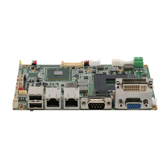
Page 15: Location Of Connectors & Jumpers
S u b C o m p a c t B o a r d G E N E - Q M 5 7 2.2 Location of Connectors and Jumpers Component Side Chapter 2 Quick Installation Guide... - Page 16 S u b C o m p a c t B o a r d G E N E - Q M 5 7 Solder Side Chapter 2 Quick Installation Guide...
-
Page 17: Mechanical Drawing
S u b C o m p a c t B o a r d G E N E - Q M 5 7 2.3 Mechanical Drawing Component Side Chapter 2 Quick Installation Guide... - Page 18 S u b C o m p a c t B o a r d G E N E - Q M 5 7 Solder Side Chapter 2 Quick Installation Guide...
-
Page 19: List Of Jumpers
S u b C o m p a c t B o a r d G E N E - Q M 5 7 2.4 List of Jumpers The board has a number of jumpers that allow you to configure your system to suit your application. -
Page 20: List Of Connectors
S u b C o m p a c t B o a r d G E N E - Q M 5 7 2.5 List of Connectors The board has a number of connectors that allow you to configure your system to suit your application. - Page 21 S u b C o m p a c t B o a r d G E N E - Q M 5 7 CN24 (LAN2) LAN Connector CN25 UIM Connector CN26 Digital I/O Connector CN28 (COM1) RS-232 Serial Port Connector CN30 (COM2) RS-232/422/485 Serial Port Connector CN32...
-
Page 22: Setting Jumpers
S u b C o m p a c t B o a r d G E N E - Q M 5 7 2.6 Setting Jumpers You configure your card to match the needs of your application by setting jumpers. A jumper is the simplest kind of electric switch. It consists of two metal pins and a small metal clip (often protected by a plastic cover) that slides over the pins to connect them. -
Page 23: Cmos Selection (Jp1)
S u b C o m p a c t B o a r d G E N E - Q M 5 7 2.7 CMOS Selection (JP1) Function Protected (Default) Clear 2.8 LVDS(1)-Inverter +5V/ +12V Selection (JP3) Function +12V +5V (Default) 2.9 LVDS(1)-Inverter Voltage/PWM Control Selection (JP4) Function... -
Page 24: Output Power Connector (Cn3)
S u b C o m p a c t B o a r d G E N E - Q M 5 7 Ring (Default) 2.13 PWM Signal Inverter/Non-Inverter Selection (JP10) JP10 Function Non-Inverter (Default) Inverter 2.14 Output Power Connector (CN3) Signal Note: The max. -
Page 25: Lvds (1)- Inverter +5V/+12V Connector (Cn6)
S u b C o m p a c t B o a r d G E N E - Q M 5 7 CRT_DDC_CLK +5V_DAC CRT_OHSYNCF CRT_GREEN CRT_PLUG# CRT_OVSYNCF CRT_BLUE CRT_DDC_DATA CRT_RED CRT_RED CRT_GREEN CRT_BLUE CRT_OHSYNCF 2.16 LVDS (1)- Inverter +5V/+12V Connector (CN6) Signal VCC-Inverter BKL_CON... - Page 26 S u b C o m p a c t B o a r d G E N E - Q M 5 7 LVDSVCC LA_DATA0- LA_DATA0 LA_DATA1- LA_DATA1 LA_DATA2- LA_DATA2 LA_DATA3- LA_DATA3 LVDS_DDC_DATA LVDS_DDC_CLK LB_DATA0- LB_DATA0 LB_DATA1- LB_DATA1 LB_DATA2- LB_DATA2 LB_DATA3- LB_DATA3...
-
Page 27: Fan Connector (Cn12)
S u b C o m p a c t B o a r d G E N E - Q M 5 7 2.19 Fan Connector (CN12) Signal +12V Speed Sense 2.20 USB Connector (CN13) Signal +5V_DUAL USB2_L1- USB2_L+ 2.21 USB Connector (CN14) Signal +5V_DUAL... -
Page 28: Usb Connector (Cn17)
S u b C o m p a c t B o a r d G E N E - Q M 5 7 2.23 USB Connector (CN17) Signal +5V_DUAL USB5_L1- USB5_L+ 2.24 USB Connector (CN18) Signal +5V_DUAL USB10_L1- USB10_L+ 2.25 USB Connector (CN19) Signal +5V_DUAL... -
Page 29: Audio 2.1 Channel Connector (Cn20)
S u b C o m p a c t B o a r d G E N E - Q M 5 7 2.26 Audio 2.1 Channel Connector (CN20) Signal MIC_L MIC_R AUD_GND LIN_L LIN_R AUD_GND LOUT_L AUD_GND LOUT_R V5_AUD_S0 2.27 Front Panel (CN21) S i g n a l... -
Page 30: Uim Connector (Cn25)
S u b C o m p a c t B o a r d G E N E - Q M 5 7 2.29 UIM Connector (CN25) Signal UIM_PWR UIM_RST UIM_CLK UIM_VPP UIM_DAT 2.30 Digital I/O Connector (CN26) This connector offers 4-pair of digital I/O functions and address is A41h. The pin definitions are illustrated below: S i g n a l P i n... -
Page 31: Rs-232/422/485 Serial Port Connector (Cn30)
S u b C o m p a c t B o a r d G E N E - Q M 5 7 Port 3 @A41h Pin 3 GPIO Set 2 / Bit 2 U03 Pin 25 (GPIO 22) Port 2 @A41h Pin 2 GPIO Set 2 / Bit 1... -
Page 32: Dvi Connector (Cn32) (Optional)
S u b C o m p a c t B o a r d G E N E - Q M 5 7 RS-422 S i g n a l P i n S i g n a l RS-485 S i g n a l P i n... -
Page 33: Power Jack Connector (Cn33)
S u b C o m p a c t B o a r d G E N E - Q M 5 7 2.34 12V Power Jack Connector (CN33) Signal +12V_EXT 2.35 Output +5V_DUAL / PSON# /SM Bus Connector (CN34) Signal SMB_DAT_A1 SMB_CLK_A1... - Page 34 S u b C o m p a c t B o a r d G E N E - Q M 5 7 Below Table for China RoHS Requirements 產品中有毒有害物質或元素名稱及含量 AAEON Main Board/ Daughter Board/ Backplane 有毒有害物質或元素 部件名稱 鉛...
-
Page 35: Chapter 3 Ami Bios Setup
S u b C o m p a c t B o a r d G E N E - Q M 5 7 Chapter BIOS Setup Chapter 3 AMI BIOS Setup 3-1... -
Page 36: System Test And Initialization
3. The CMOS memory has lost power and the configuration information has been erased. The GENE-QM57 CMOS memory has an integral lithium battery backup for data retention. However, you will need to replace the complete unit when it finally runs down. -
Page 37: Ami Bios Setup
S u b C o m p a c t B o a r d G E N E - Q M 5 7 3.2 AMI BIOS Setup AMI BIOS ROM has a built-in Setup program that allows users to modify the basic system configuration. -
Page 38: Chapter 4 Driver Installation
S u b C o m p a c t B o a r d G E N E - Q M 5 7 Chapter Driver Installation 4 -1 Chapter 4 Driver Installation... - Page 39 S u b C o m p a c t B o a r d G E N E - Q M 5 7 The GENE-QM57 comes with a CD-ROM that contains all drivers your need. Follow the sequence below to install the drivers: Step 1 –...
- Page 40 S u b C o m p a c t B o a r d G E N E - Q M 5 7 4.1 Installation: Insert the GENE-QM57 DVD-ROM into the DVD-ROM Drive. And install the drivers from Step 1 to Step 7 in order. Step 1 – Install Chipset Driver 1.
- Page 41 S u b C o m p a c t B o a r d G E N E - Q M 5 7 Step 4 – Install ME Driver 1. Click on the STEP4-ME folder and select the OS your system is 2.
-
Page 42: Appendix A Programming The Watchdog Timer
S u b C o m p a c t B o a r d G E N E - Q M 5 7 Appendix Programming the Watchdog Timer Appendix A Programming the Watchdog Timer... -
Page 43: Programming
S u b C o m p a c t B o a r d G E N E - Q M 5 7 A.1 Programming GENE-QM57 utilizes ITE 8712 chipset as its watchdog timer controller. Below are the procedures to complete its configuration and the AAEON intial watchdog timer program is also attached based on which you can develop customized program to fit your application. - Page 44 S u b C o m p a c t B o a r d G E N E - Q M 5 7 Mode is not exited normally. (1) Enter the MB PnP Mode To enter the MB PnP Mode, four special I/O write operations are to be performed during Wait for Key state.
- Page 45 S u b C o m p a c t B o a r d G E N E - Q M 5 7 WatchDog Timer Configuration Registers Configure Control (Index=02h) This register is write only. Its values are not sticky; that is to say, a hardware reset will automatically clear the bits, and does not require the software to clear them.
- Page 46 S u b C o m p a c t B o a r d G E N E - Q M 5 7 WatchDog Timer Configuration Register (Index=72h, Default=00h) WatchDog Timer Time-out Value Register (Index=73h, Default=00h) Appendix A Programming the Watchdog Timer...
-
Page 47: Ite8712 Watchdog Timer Initial Program
S u b C o m p a c t B o a r d G E N E - Q M 5 7 A.2 ITE8712 Watchdog Timer Initial Program .MODEL SMALL .CODE Main: CALL Enter_Configuration_mode CALL Check_Chip mov cl, 7 call Set_Logic_Device ;time setting mov cl, 10 ;... - Page 48 S u b C o m p a c t B o a r d G E N E - Q M 5 7 ; game port enable mov cl, 9 call Set_Logic_Device Initial_OK: CALL Exit_Configuration_mode MOV AH,4Ch INT 21h Enter_Configuration_Mode PROC NEAR MOV SI,WORD PTR CS:[Offset Cfg_Port] MOV DX,02Eh...
- Page 49 S u b C o m p a c t B o a r d G E N E - Q M 5 7 Exit_Configuration_Mode ENDP Check_Chip PROC NEAR MOV AL,20h CALL Read_Configuration_Data CMP AL,87h JNE Not_Initial MOV AL,21h CALL Read_Configuration_Data CMP AL,12h JNE Not_Initial Need_Initial:...
- Page 50 S u b C o m p a c t B o a r d G E N E - Q M 5 7 MOV DX,WORD PTR CS:[Cfg_Port+06h] IN AL,DX Read_Configuration_Data ENDP Write_Configuration_Data PROC NEAR MOV DX,WORD PTR CS:[Cfg_Port+04h] OUT DX,AL XCHG AL,AH MOV DX,WORD PTR CS:[Cfg_Port+06h] OUT DX,AL...
- Page 51 S u b C o m p a c t B o a r d G E N E - Q M 5 7 Set_Logic_Device proc near push ax push cx xchg al,cl mov cl,07h call Superio_Set_Reg pop cx pop ax Set_Logic_Device endp ;Select 02Eh->Index Port, 02Fh->Data Port Cfg_Port DB 087h,001h,055h,055h...
-
Page 52: Appendix B I/O Information
S u b C o m p a c t B o a r d G E N E - Q M 5 7 Appendix I/O Information B - 1 Appendix B I/O Information... -
Page 53: I/O Address Map
S u b C o m p a c t B o a r d G E N E - Q M 5 7 B.1 I/O Address Map B - 2 Appendix B I/O Information... -
Page 54: Memory Address Map
S u b C o m p a c t B o a r d G E N E - Q M 5 7 B.2 Memory Address Map B - 3 Appendix B I/O Information... -
Page 55: Irq Mapping Chart
S u b C o m p a c t B o a r d G E N E - Q M 5 7 B.3 IRQ Mapping Chart B.4 DMA Channel Assignments B - 4 Appendix B I/O Information... - Page 56 S u b C o m p a c t B o a r d G E N E - Q M 5 7 Appendix Mating Connecotor C - 1 Appendix C Mating Connector...
-
Page 57: Appendix C Mating Connector
S u b C o m p a c t B o a r d G E N E - Q M 5 7 C.1 List of Mating Connectors and Cables The table notes mating connectors and available cables. Mating Connector Connector Available Cable P/N... - Page 58 S u b C o m p a c t B o a r d G E N E - Q M 5 7 and MIC Connector Keyboard / KB/MS CN22 Mouse Wafer B6B-PHDSS 1700060152 Connector Cable RJ-45 CN23 Ethernet#1 Neltron 7001-8P8C Connector...
- Page 59 S u b C o m p a c t B o a r d G E N E - Q M 5 7 A ppendix RAID & AHCI Settings Appendix D RAID & AHCI Settings...
-
Page 60: Setting Raid
S u b C o m p a c t B o a r d G E N E - Q M 5 7 D.1 Setting RAID OS installation to setup RAID Mode Step 1: Copy the files below from “Driver CD -> Raid Driver -> F6 Floppy - x86”... - Page 61 S u b C o m p a c t B o a r d G E N E - Q M 5 7 Step 3: The setting procedures “ In BIOS Setup Menu” A: Advanced -> SATA Configuration -> SATA Mode -> RAID Mode Step 4: The setting procedures “In BIOS Setup Menu”...
- Page 62 S u b C o m p a c t B o a r d G E N E - Q M 5 7 Step 5: The setting procedures “In BIOS Setup Menu” C: Boot -> Boot Option #1 -> DVD-ROM Type Step 6: The setting procedures “In BIOS Setup Menu”...
- Page 63 S u b C o m p a c t B o a r d G E N E - Q M 5 7 Step 7: Press Ctrl-I to enter MAIN MENU Step 8: Choose “1.Create RAID Volume” Appendix D RAID & AHCI Settings...
- Page 64 S u b C o m p a c t B o a r d G E N E - Q M 5 7 Step 9: RAID Level -> RAID0(Stripe) Step 10: Choose “Create Volume” Appendix D RAID & AHCI Settings...
- Page 65 S u b C o m p a c t B o a r d G E N E - Q M 5 7 Step 11: Choose “Y” Step 12: Choose “5. Exit” Appendix D RAID & AHCI Settings...
- Page 66 S u b C o m p a c t B o a r d G E N E - Q M 5 7 Step 13: Choose “Y” Step 14: Setup OS Appendix D RAID & AHCI Settings...
- Page 67 S u b C o m p a c t B o a r d G E N E - Q M 5 7 Step 15: Press “F6” Step 16: Choose “S” Appendix D RAID & AHCI Settings...
- Page 68 S u b C o m p a c t B o a r d G E N E - Q M 5 7 Step 17: Choose “Intel(R) ICH8M-E/ICH9M-E/5 Series SATA RAID Controller” Step 18: It will show the model number you select and then press “ENTER” D-10 Appendix D RAID &...
- Page 69 S u b C o m p a c t B o a r d G E N E - Q M 5 7 Step 19: Setup is starting Windows D-11 Appendix D RAID & AHCI Settings...
-
Page 70: Setting Ahci
S u b C o m p a c t B o a r d G E N E - Q M 5 7 D.2 Setting AHCI OS installation to setup AHCI Mode Step 1: Copy the files below from “Driver CD -> Raid Driver -> F6 Floppy - x86”... - Page 71 S u b C o m p a c t B o a r d G E N E - Q M 5 7 Step 3: The setting procedures “ In BIOS Setup Menu” A: Advanced -> SATA Configuration -> SATA Configuration -> SATA Mode ->...
- Page 72 S u b C o m p a c t B o a r d G E N E - Q M 5 7 Step 5: The setting procedures “In BIOS Setup Menu” C: Save & Exit -> Save Changes and Exit Step 6: Setup OS D-14 Appendix D RAID &...
- Page 73 S u b C o m p a c t B o a r d G E N E - Q M 5 7 Step 7: Press “F6” Step 8: Choose “S” D-15 Appendix D RAID & AHCI Settings...
- Page 74 S u b C o m p a c t B o a r d G E N E - Q M 5 7 Step 9: Choose “Intel(R) 5 Series 6 Port SATA AHCI Controller” tep 10: It will show the model number you select and then press “ENTER” D-16 Appendix D RAID &...
- Page 75 S u b C o m p a c t B o a r d G E N E - Q M 5 7 Step 11: Setup is loading files D-17 Appendix D RAID & AHCI Settings...
Need help?
Do you have a question about the GENE-QM57 and is the answer not in the manual?
Questions and answers