Table of Contents
Advertisement
Quick Links
Download this manual
See also:
Command Manual
Advertisement
Table of Contents

Related Manuals for Neoway WM620


Summary of Contents for Neoway WM620
- Page 1 WM620 Hardware User Guide Version 1.7...
- Page 2 Neoway provides customers complete technical support. If you have any question, please contact your account manager or email to the following email addresses: Sales@neoway.com...
- Page 3 Added description of LED status V1.5 Deleted WM620-B 2015-07 Added response time in sleep mode Added WM620-B and deleted HSDPA Modified pin definition figure and recommended PCB foot print Modified the recommended level shifting circuit V1.6 2017-04 ...
-
Page 4: Table Of Contents
WM620 Hardware User Guide Contents 1 Introduction to WM620 ....................1 1.1 Overview ............................1 1.2 Block Diagram ........................... 1 1.3 Specifications ............................. 2 2 Pin Description and PCB Foot Print ................4 2.1 Specifications ............................. 4 2.2 Pin Definition ............................. 5 2.3 PCB Foot Print ........................... - Page 5 5.2 Temperature ............................32 5.3 Current .............................. 32 5.4 ESD Protection ..........................33 6 Typical Circuits ........................ 34 7 Mounting the Module onto the Application Board ..........36 8 Package ..........................37 9 Abbreviations ........................38 Copyright © Neoway Technology Co., Ltd...
- Page 6 Table of Figures Figure 2-1 Bottom view of the WM620 module ..................4 Figure 2-2 PCB foot print recommended for WM620 (unit: mm) ............7 Figure 3-1 Current peaks and voltage drops ................... 9 Figure 3-2 Power supply design ......................9 Figure 3-3 Reference design of power supply controlled by MIC29302 ..........
- Page 7 WM620 Hardware User Guide Table of Tables Table 1-1 WM620 specifications ......................2 Table 2-1 WM620 pin definition......................5 Table 3-1 Power supply and switch interface ..................8 Table 3-2 Capacity matching power failure duration ................12 Table 3-3 LED indicator ........................15 Table 3-4 Network status indication (a) ....................
-
Page 8: Introduction To Wm620
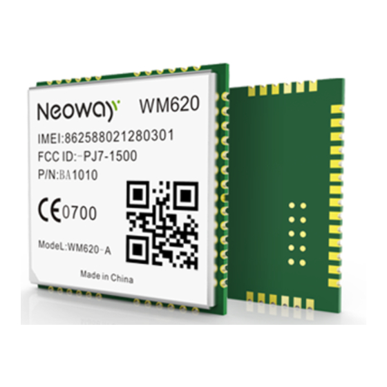
SMS and other functions. It is widely applied to electricity, Internet of Vehicle (IoV), video monitoring, handset devices, etc. WM620 is an SMT module in LCC compact package. It can be easily adopted for standard Mini PCI-E interface. The model of WM620 is shown as follows. -
Page 9: Specifications
Operating Voltage 3.3 V to 4.2 V DC (recommended 3.9 V, 25° C) GSM07.07 AT Command Neoway extended AT commands (Refer to Neo_WM620 WCDMA Module AT Command Set) Driver Supporting Windows XP, Windows 7, Linux(2.6.1) GSM: FR, EFR, HR, AMR Voice Coding, DTMF... - Page 10 WM620 Hardware User Guide Call Forwarding (CFB, CFNA, CFU) Supplementary Service Call Waiting Three-Way Calling Copyright © Neoway Technology Co., Ltd...
-
Page 11: Pin Description And Pcb Foot Print
2.1 Specifications Specifications WM620 Dimensions 30± 0.1 mm x 30± 0.1 mm x 2.7± 0.1 mm (H x W x D) Weight Encapsulation 62-pin LCC Figure 2-1 Bottom view of the WM620 module ANT_M SPK_N SPK_P MIC_2P MIC_2N POWER Audio... -
Page 12: Pin Definition
For more details about pins, see the pin description. JTAG pins have not be open to customers. 2.2 Pin Definition Table 2-1 WM620 pin definition Level Pin No. Pin Name Function Remarks Feature (V) - Page 13 SMS and Incoming Call Ring Indicating an incoming RING VDD_2.6V call or message Sleep Mode Controlling Controlling sleep SLEEP_IN VDD_1.8V mode Voltage range: 0 V 12-bit ADC input to 2.2 V Reserved Pins 2-11, 37-42, 56-59, 62 Copyright © Neoway Technology Co., Ltd...
-
Page 14: Pcb Foot Print
WM620 Hardware User Guide 2.3 PCB Foot Print LCC packaging is adopted to package the pins of the WM620 module. Figure 2-2 shows the recommended PCB foot print. Figure 2-2 PCB foot print recommended for WM620 (unit: mm) Copyright © Neoway Technology Co., Ltd... -
Page 15: Interface Design
VRTC RTC power supply input/output Not used for any other functions Ensure that the VBAT never exceeds 4.5 V DC. Voltage higher than 4.5 V DC may damage the WM620 module. 3.1.1 VBAT VBAT is the main power supply of the module. Its input voltage ranges from 3.3 V to 4.2 V and the preferable value is 3.9 V. -
Page 16: Figure 3-1 Current Peaks And Voltage Drops
In addition, add 0.1 μF, 100 pF, and 33 pF filter capacitors to filter high frequency interference. A controllable power supply is preferable if the module is used in harsh conditions. The WM620 module might fail to reset in remote or unattended applications, or in an environment with great electromagnetic interference (EMI). -
Page 17: Figure 3-3 Reference Design Of Power Supply Controlled By Mic29302
In the above circuit, Q2 is added to eliminate the need for a high enough voltage level of the host GPIO. In case that the GPIO can output a high voltage greater than VDD_3.9V - |V |, where V is the GS(th) GS(th) Gate Threshold Voltage, Q2 is not needed. Copyright © Neoway Technology Co., Ltd... -
Page 18: Vrtc
Figure 3-5 RTC reference design WM620 VRTC Circuit Backup Capacitor Battery The capacity of the supercapacitor is dependent on the duration of exceptional power failures. Table 3-2 shows the capacity matching the power failure duration. Copyright © Neoway Technology Co., Ltd... -
Page 19: Vdd
200KΩ resistor and controlled by external OC. Figure 3-7 shows its pulse width and power-on procedure. When the WM620 is powered on, the VDD_2.6V pin will be pulled up and keep 2.6 V DC output. The UART will send +EIND:8 after the module is powered on properly and send +EUSIM:1 after the USIM card is identified. -
Page 20: Figure 3-6 Reference Circuit Of On_Off Controlled By High Level
The shutdown function of the ON_OFF pin is controlled by the software. If the software is not running properly, the module cannot shut down properly. Figure 3-7 shows the power-on procedure of the WM620 module. Figure 3-7 Power-on procedure VBAT 1.6V<V... -
Page 21: Reset
RESET is a hard reset input pin that is pulled up internally by a resistance and activated by low level signal. Low level pulse longer than 20 ms can reset the WM620 module. After resetting the module, power on the module again. The recommended reset pulse is 50 ms, and it cannot exceed 2 seconds. Otherwise, the WM620 module will be powered off. -
Page 22: Running Status Indication
The LED can be directly connected to this pin with a resistor in series. For better luminance, drive the LED with a transistor instead. The LED's brightness depends on the value of R1 and VCC. Copyright © Neoway Technology Co., Ltd... -
Page 23: Ring Pin
RING pin outputs 250 ms high-level pulses at 4s period. After the call is answered, the low-level pulse restores. Figure 3-11 RING indicator for incoming call 250ms 250ms SMS: Upon receipt of SMS, the module outputs one 600 ms high-level pulse. Figure 3-12 RING indicator for SMS 600 ms Copyright © Neoway Technology Co., Ltd... -
Page 24: Usim Card Interface
SIM card data input/output 1.8/3.0 V WM620 supports 3.0 V and 1.8 V USIM cards. USIM_DATA need to be externally pulled up to USIM_VCC by a 10 KΩ resistor. USIM_CLK works at 3.25MHz typically. Figure 3-13 Reference design of USIM card interface... -
Page 25: Figure 3-14 Recommended Esd Diode Array
Ensure as short PCB traces of USIM_DATA and USIM CLK as possible and surround the traces with GND copper. RF traces or RF connector should be far away from the USIM card and USIM card traces. Copyright © Neoway Technology Co., Ltd... -
Page 26: Usb Interfaces
USB Power Input voltage 3.3 to 5.5 V. The WM620 module is compliant with USB 2.0 full speed device. The USB 2.0 specification requires that the hosts such as computers support three USB speeds: low-speed (1.5 Mbit/s), full-speed (12 Mbit/s) and high-speed (480 Mbit/s). -
Page 27: Uart
UART is used for AT commands, data sending/receiving, etc. The UART of WM620 works at 2.6 V CMOS logic level. The voltages for input high level should not exceed 3.0 V. Supported baud rates are 300, 600, 1200, 2400, 4800, 9600, 14400, 19200, 38400, 57600, 115200, 230400, 460800, 921600 bit/s, and the default rate is 115200 bit/s. -
Page 28: Level Shifting For Uart
33 pF MCU_URXD 33 pF If the UART is interfaced with an MCU that has 5 V logic levels, level shifting is required for both UART receive and transmit. Figure 3-19 shows a reference circuit. Copyright © Neoway Technology Co., Ltd... -
Page 29: Sleep Mode
Do not send any data to UART within 5 seconds after the module is turned on. 3.6 Sleep Mode The sleep mode of WM620 is controlled in two ways: UART and USB. The module can receive voice and SMS message in sleep mode controlled by UART or USB. Upon receiving SMS messages, voice, or data,... -
Page 30: Uart Control
If the module (DCE) communicates with DTE via USB port, the following two methods are recommended to bring the module into the sleep mode. When the DTE supports the Suspend state of USB ports, use the design in Figure 3-21. Copyright © Neoway Technology Co., Ltd... -
Page 31: Figure 3-21 Sleep Mode Controlled By Usb (A)
The module can receives voice, SMS, and other messages in the sleep mode enabled by UART and USB. It wakes up automatically upon receiving SMS, voice, or data. Then send AT commands. The module enters the sleep mode again after all services are over. Copyright © Neoway Technology Co., Ltd... -
Page 32: Audio Interface
Neo_WM620 WCDMA Module AT Command Set. The following figures shows typical audio interfaces of WM620. The earphone output pins are directly connected to the receiver. Parallel a bypass capacitor for each pin. The capacitor of 100 pF or less is expected to optimize performance in each design. -
Page 33: Figure 3-24 Reference Design Of Single-End Input Mic Interface
33 pF 10 pF Figure 3-26 Reference design for speaker single-ended output SPK_P 33 pF 10 pF Speaker 8-Ohms SPK_N WM620 Table 3-10 MIC voltage and current Min. Typical Max. Unit MIC voltage 1.75 1.85 Copyright © Neoway Technology Co., Ltd... -
Page 34: Adc
12-bit digit signals. Users can use the AT+GETADC command to query. For more information, refer to Neo_WM620 WCDMA Module AT command Set. Copyright © Neoway Technology Co., Ltd... -
Page 35: Rf Interface
0.8 mm to 1.0 mm; the RF is 1 mm away from the ground. Figure 3-28 shows a two-layer board application. The RF is connected to GSC RF connector through traces on PCB, which is connected to the antenna via cable. Figure 3-28 RF layout reference Copyright © Neoway Technology Co., Ltd... - Page 36 WM620 Hardware User Guide On the PCB, keep the RF signals and RF components away from high-speed circuits, power supplies, transformers, great inductors, the clock circuit of single-chip host, etc. Copyright © Neoway Technology Co., Ltd...
-
Page 37: Rf Features
4.2.2 Receiving Sensitivity Receiving sensitivity is another important performance indicator of the wireless modules. It measures the module's capability to receive weak signals. Table 4-3 lists WM620 data obtained in lab tests for different bands and corresponding 3GPP standards. Copyright © Neoway Technology Co., Ltd... -
Page 38: Table 4-3 Receiving Sensitivity (Unit: Dbm)
Band VIII (BER<0.1%) < -104.7 -108 -106 The data in the above tables is obtained by connecting the module to RF test instrument (e.g. CMU200, CWM500, or Agilent8960) in lab tests. It is for reference only. Copyright © Neoway Technology Co., Ltd... -
Page 39: Electric Features And Reliability
25 ° C +85 ° C 5.3 Current Table 5-3 and Table 5-4 lists the current of WM620 in different modes at 25 º C and 3.9V. During the test, the USB is disconnected. Table 5-3 Operating current (Unit: mA) -
Page 40: Esd Protection
Contact Discharge Air Discharge VBAT, GND ± 8 kV ± 15 kV USB, UART ± 4 kV ± 8 kV Antenna ± 8 kV ± 15 kV Other Interfaces ± 2 kV ± 4 kV Copyright © Neoway Technology Co., Ltd... -
Page 41: Typical Circuits
MCU ON_OFF 10 nF R6 and C3 are close to the pin. RESET WM620 MCU RESET 10nF MIC1_P 100 pF MIC1_N EAR_P 100 pF EAR_N 100 pF 100 pF CON-RJ11 100 pF 100 pF Copyright © Neoway Technology Co., Ltd... - Page 42 0.1 uF 1000 uF 100 uF 100 pF SIG_LED C25 4.7 uF 100 pF RF_ANT_F 2.0pF 2.0pF SPKR_N SPKR_N SPKR_P SPKR_P MIC2_N MIC2_N MIC2_P MIC2_P C4 100 pF 0.1 uF 100 uF 1000 uF Copyright © Neoway Technology Co., Ltd...
-
Page 43: Mounting The Module Onto The Application Board
WM620 Hardware User Guide 7 Mounting the Module onto the Application Board WM620 is compatible with industrial standard reflow profile for lead-free SMT process. The reflow profile is process dependent, so the following recommendation is just a start point guideline: ... -
Page 44: Package
WM620 Hardware User Guide 8 Package WM620 modules are packaged in sealed bags on delivery to guarantee a long shelf life. Follow the same package method again in case of opened for any reasons. If the module is exposed to air for more than 48 hours at conditions not worse than 30° C/60% RH, bake it at a temperature higher than 90 degree for more than 12 hours before SMT. -
Page 45: Abbreviations
Electro Magnetic Interference Electronic Static Discharge European Telecommunication Standard FDMA Frequency Division Multiple Access Full Rate GPRS General Packet Radio Service Global Standard for Mobile Communications Half Rate Integrated Circuit IMEI International Mobile Equipment Identity Copyright © Neoway Technology Co., Ltd... - Page 46 Read-only Memory Root Mean Square Real Time Clock Subscriber Identification Module Short Message Service SRAM Static Random Access Memory Terminal adapter TDMA Time Division Multiple Access UART Universal asynchronous receiver-transmitter VSWR Voltage Standing Wave Ratio Copyright © Neoway Technology Co., Ltd...
Need help?
Do you have a question about the WM620 and is the answer not in the manual?
Questions and answers