
Related Manuals for Neoway M660


Summary of Contents for Neoway M660
- Page 1 M660 GPRS Module User Manual Shenzhen Neoway Technology Co.,Ltd. Enjoy your wireless life...
- Page 2 This document is intended for the customer engineers. This document is subject to change without any notice. No responsibility is assumed by Neoway Technology for the use of this document. Neoway Technology always provides the best supports. For pricing, ordering information and delivery please contact: Sales@neoway.com.cn...
-
Page 3: Table Of Contents
RING ........................21 SIM interface ........................21 Running LED Indicator ....................... 23 Audio Interface ........................24 Antenna Interface ........................ 26 Mounting the Module onto the Application Board ............... 28 Package ............................. 29 Shenzhen Neoway Technology Co., Ltd. Page 3 of 32... - Page 4 Terms and Abbreviations ......................29 Shenzhen Neoway Technology Co., Ltd. Page 4 of 32...
-
Page 5: Revision History
Document History Revision History Version Remarks Date Issue V3.0 Modified Version 2013-9 V3.1 Change receive sensitivity index 2013-10 V3.2 Change 24pin definition 2013-11 Shenzhen Neoway Technology Co., Ltd. Page 5 of 32... -
Page 6: Introduction
2. General Description With the ultra-compact design, M660 is intended to be used in a wide range of applications, including industrial and consumer devices. M660 is a GSM/GPRS module with EDGE of downlink. It features with voice, SMS, and data services. -
Page 7: Key Features
4. Key Features Table1 M660 Key Features Feature Implementation Frequency Bands 850/900/1800/1900 MHz Quad-band Compliant with GSM/GPRS Phase2/2+ Sensitivity < -107dBm 850/900 Class4(2W) Transmit Power 1800/1900 Class1(1W) GSM07.07 Extended AT commands Audio CODEC FR、EFR、HR、AMR TEXT/PDU Point-to-point / cell broadcast DATA GPRS:Class 12 Call forwarding(CFB, CFNA, CFU)... -
Page 8: Product Specifications
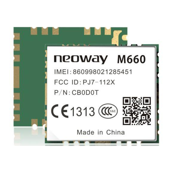
5.1 Variants Variants Frequencies Packages M660-QUAD-AA0/A00 850/900/1800/1900MHz Quad-band 28 Pin LCC 5.2 Dimension & Package Physical Characteristics Dimensions 22mm*18.4mm*2.7mm (Length*Width*Thickness) Weight 2.2 g Package 28 Pin LCC Figure 2 M660 Sketch Shenzhen Neoway Technology Co., Ltd. Page 8 of 32... -
Page 9: Pin Description
5.3 Pin Description Table2 M660 pin definition M660 Signal Function Note VSIM SIM supply voltage 1.8/3.0V compatible. SIM_CLK SIM clock 5KΩ internal pull-up SIM_DATA SIM data SIM_RST SIM reset Prompted by module Vi ≤ 200mVpp MICP MIC+ MICN MIC- Vi ≤ 200mVpp Signal Ended Output. -
Page 10: Pcb Foot Print
5.4 PCB foot print Recommended foot print: Figure 3 Recommended foot print of M660 (all dimensions in millimeters) Note: Every other pitch not specified is 2.0mm. The circle on the top-right with a 1.3mm radius, defines a keep-out region, under which any copper or wire is inhibited, due to the RF test point here needs to be surrounded by restricted area filled with air. -
Page 11: Application Interface
It’s very important to ensure that the voltage of supply rail never drops below 3.5V while any burst occurs. Figure 4 shows how the GSM bursts and voltage drops. Figure 5 shows how the capacitor helps to improve peak current performance. Shenzhen Neoway Technology Co., Ltd. Page 11 of 32... - Page 12 Use a low impedance power source, and keep the resistance of the power supply lines as low as possible. Shenzhen Neoway Technology Co., Ltd. Page 12 of 32...
-
Page 13: Extended Design Rules For Power Supply
GPRS_EN signal is routed to host GPIO, controlling the ON/OFF of the P-MOSFET. The host can cut off and then switch on the power supply in case of abnormal conditions, such as no response from the module or the disconnection of GPRS. Shenzhen Neoway Technology Co., Ltd. Page 13 of 32... - Page 14 The module shall be supplied by an independent power, like a DC/DC or LDO. The inductor used in Reference Design (b), should be a power inductor and have a very low Shenzhen Neoway Technology Co., Ltd. Page 14 of 32...
-
Page 15: On/Off Procedure
Prior to turning on the module, turn on the host MCU and finish the UART initialization. Otherwise conflictions may occur during initialization, due to unstable conditions. 6.2 ON/OFF Procedure ON/OFF is a low level pulse active input, used to turn on or off the module. Shenzhen Neoway Technology Co., Ltd. Page 15 of 32... -
Page 16: Turning On The Module
1 second later it will shut down. Another approach to turn off the module is with AT command. Figure 10 shows a reference circuits for ON/OFF control with inverted control logic. Shenzhen Neoway Technology Co., Ltd. Page 16 of 32... -
Page 17: Reset
VCCIO is provided to power the level translators, with a 2.8V / 5mA output. VCCIO can also be used to monitor the on/off state of module. It outputs 2.8V high level while the module is on, and low level while the module is off. Shenzhen Neoway Technology Co., Ltd. Page 17 of 32... -
Page 18: Uart
Supported baud rates are 1200, 2400, 4800, 9600, 19200, 38400, 57600, 115200, 230400bps, and the default is 115200. Figure 11 Connection between DCE (module) and DTE The UART of M660 works at 2.8V CMOS logic level. The voltages for input high level should not exceed 3.0V. 6.3.2 Level Translators for UART If the UART is interfacing with a MCU that has 3.3V logic levels, resistors should be connected in... - Page 19 It can be used between module UTXD1 and MCU RXD as well, with INPUT connected to module UTXD1, and OUTPUT connected to MCU RXD. VCC_IN powered from 2.8V (module’s VCCIO) and VCC_OUT powered from 5V. This applies to RING signal as well. Shenzhen Neoway Technology Co., Ltd. Page 19 of 32...
-
Page 20: Sleep Mode
And then the host MCU can process the voice call, received data, or SMS. After processing is finished, pull DTR low again to put the module into sleep mode. Shenzhen Neoway Technology Co., Ltd. Page 20 of 32... -
Page 21: Ring
Figure 15 RING Indicator for SMS 6.5 SIM interface Table5 SIM Interface Signal Function Note VSIM SIM supply voltage 1.8/3.0V SIM_CLK SIM clock SIM_RST SIM reset SIM_DATA SIM data Internal pull up Shenzhen Neoway Technology Co., Ltd. Page 21 of 32... - Page 22 Figure 16b a sample of SIM card socket Figure 16c the recommended ESD diode array M660 SIM interface is 3V/1.8V compatible. VSIM is for SIM power and can supply a 30mA current. SIM_DATA is internally pulled up with a 5KΩ resistor. External pull-up resistor is not needed.
-
Page 23: Running Led Indicator
It can output a 4mA current and 2.8V voltage, therefore a LED can be directly connected to this pin with a resistor in series. For better luminance, drive the LED with a transistor instead, see Figure 17. Figure 17 LED Indicator Shenzhen Neoway Technology Co., Ltd. Page 23 of 32... -
Page 24: Audio Interface
C1 and C2, should be placed between the outputs of amplifier and module, to block the bias voltage. For a peak-peak voltage greater than 200mV, an attenuation circuit comprised of R1-R4 should be used. Shenzhen Neoway Technology Co., Ltd. Page 24 of 32... - Page 25 To pass the low frequency audio, use large capacitors for C1 and C2. If an external amplifier is used for driving the speakers, 1uF~4.7uF coupling capacitors should be used to block the DC voltage, as shown in Figure 21. Shenzhen Neoway Technology Co., Ltd. Page 25 of 32...
-
Page 26: Antenna Interface
The trace should be surrounded by ground copper. Place plenty of via holes to connect this ground copper to main ground plane, at the copper edge. Shenzhen Neoway Technology Co., Ltd. Page 26 of 32... - Page 27 Avoid any other traces crossing the antenna trace on neighboring layer. Figure 22 Reference design for antenna interface Figure 23 Reference parameters for 50Ω trace on a 1.6mm double layer PCB Shenzhen Neoway Technology Co., Ltd. Page 27 of 32...
-
Page 28: Mounting The Module Onto The Application Board
Figure 24 Reference layout for antenna interface 7. Mounting the Module onto the Application Board M660 is compatible with industrial standard reflow profile for lead-free SMT process. The reflow profile is process dependent, so the following recommendation is just a start point guideline: ... -
Page 29: Package
8. Package M660 modules are packaged in sealed bags on delivery to guarantee a long shelf life. Package the modules again in case of opening for any reasons. If exposed in air for more than 48 hours at conditions not worse than 30° C/60% RH, a baking procedure should be done before SMT. - Page 30 TDMA Time Division Multiple Access UART Universal asynchronous receiver-transmitter Voltage Dependent Resistor Varistor VSWR Voltage Standing Wave Ratio Shenzhen Neoway Technology Co., Ltd. Page 30 of 32...
- Page 31 & your body. IMPORTANT NOTE: This module is intended for OEM integrator. The OEM integrator is still responsible for the FCC compliance requirement of the end product, which integrates this module. Shenzhen Neoway Technology Co., Ltd. Page 31 of 32...
- Page 32 FCC RF exposure guidelines. The end product with an embedded M660 Module may also need to pass the FCC Part 15 unintentional emission testing requirements and be properly authorized per FCC Part 15.
Need help?
Do you have a question about the M660 and is the answer not in the manual?
Questions and answers