Table of Contents
Advertisement
Quick Links
Features
•
High-performance, Low-power AVR 8/16-bit XMEGA Microcontroller
•
Non-volatile Program and Data Memories
– 64K - 256K Bytes of In-System Self-Programmable Flash
– 4K - 8K Boot Code Section with Independent Lock Bits
– 2K - 4K Bytes EEPROM
– 4K - 16K Bytes Internal SRAM
External Bus Interface for up to 16M bytes SRAM
External Bus Interface for up to 128M Bytes SDRAM
•
Peripheral Features
– Four-channel DMA Controller with support for external requests
– Eight-channel Event System
– Seven 16-bit Timer/Counters
Four Timer/Counters with 4 Output Compare or Input Capture channels
Three Timer/Counters with 2 Output Compare or Input Capture channels
High Resolution Extensions on all Timer/Counters
Advanced Waveform Extension on one Timer/Counter
– Seven USARTs
IrDA Extension on 1 USART
– AES and DES Crypto Engine
– Two Two-wire Interfaces with dual address match(I
– Three SPI (Serial Peripheral Interfaces)
– 16-bit Real Time Counter with Separate Oscillator
– Two Eight-channel, 12-bit, 2 Msps Analog to Digital Converters
– One Two-channel, 12-bit, 1 Msps Digital to Analog Converter
– Four Analog Comparators with Window compare function
– External Interrupts on all General Purpose I/O pins
– Programmable Watchdog Timer with Separate On-chip Ultra Low Power Oscillator
•
Special Microcontroller Features
– Power-on Reset and Programmable Brown-out Detection
– Internal and External Clock Options with PLL
– Programmable Multi-level Interrupt Controller
– Sleep Modes: Idle, Power-down, Standby, Power-save, Extended Standby
– Advanced Programming, Test and Debugging Interfaces
JTAG (IEEE 1149.1 Compliant) Interface for test, debug and programming
PDI (Program and Debug Interface) for programming, test and debugging
•
I/O and Packages
– 50 Programmable I/O Lines
– 64-lead TQFP
– 64-pad MLF
•
Operating Voltage
– 1.6 – 3.6V
•
Speed performance
– 0 – 12 MHz @ 1.6 – 3.6V
– 0 – 32 MHz @ 2.7 – 3.6V
Typical Applications
•
Industrial control
•
Factory automation
•
Building control
•
Board control
•
White Goods
•
•
Climate control
•
•
ZigBee
•
•
Motor control
•
•
Networking
•
•
Optical
2
C and SMBus compatible)
Hand-held battery applications
Power tools
HVAC
Metering
Medical Applications
8/16-bit
XMEGA A3
Microcontroller
ATxmega256A3
ATxmega192A3
ATxmega128A3
ATxmega64A3
Preliminary
8068C–AVR–06/08
Advertisement
Table of Contents

Related Manuals for Atmel XMEGA A3 series


Summary of Contents for Atmel XMEGA A3 series
-
Page 1: Features
Features • High-performance, Low-power AVR 8/16-bit XMEGA Microcontroller • Non-volatile Program and Data Memories – 64K - 256K Bytes of In-System Self-Programmable Flash – 4K - 8K Boot Code Section with Independent Lock Bits – 2K - 4K Bytes EEPROM –... -
Page 2: Ordering Information
Notes: This device can also be supplied in wafer form. Please contact your local Atmel sales office for detailed ordering information. Pb-free packaging, complies to the European Directive for Restriction of Hazardous Substances (RoHS directive). Also Halide free and fully Green. -
Page 3: Overview
Flash section is updated, providing true Read-While-Write operation. By combining an 8/16-bit RISC CPU with In-System Self-Programmable Flash, the Atmel XMEGA A3 is a power- ful microcontroller family that provides a highly flexible and cost effective solution for many embedded applications. -
Page 4: Block Diagram
XMEGA A3 Block Diagram Figure 3-1. XMEGA A3 Block Diagram PR[0..1] XTAL1 XTAL2 Oscillator Watchdog Circuits/ Oscillator Real Time Clock Counter Generation Watchdog Timer DATA BUS Power Event System Oscillator Supervision Controller Control PA[0..7] PORT A (8) POR/BOD & RESET SRAM Sleep RESET/... -
Page 5: Resources
The XMEGA A application notes contain example code and show applied use of the modules and peripherals. The XMEGA A Manual and Application Notes are available from http://www.atmel.com/avr. 5. Disclaimer For devices that are not available yet, typical values contained in this datasheet are based on simulations and characterization of other AVR XMEGA microcontrollers manufactured on the same process technology. -
Page 6: Avr Cpu
XMEGA A3 6. AVR CPU Features • 8/16-bit high performance AVR RISC Architecture – 138 instructions – Hardware multiplier • 32x8-bit registers directly connected to the ALU • Stack in RAM • Stack Pointer accessible in I/O memory space • Direct addressing of up to 16M bytes of program and data memory •... -
Page 7: Register File
XMEGA A3 This concept enables instructions to be executed in every clock cycle. The program memory is In-System Re-programmable Flash memory. Register File The fast-access Register File contains 32 x 8-bit general purpose working registers with a single clock cycle access time. This allows single-cycle Arithmetic Logic Unit (ALU) operation. In a typ- ical ALU operation, two operands are output from the Register File, the operation is executed, and the result is stored back in the Register File - in one clock cycle. -
Page 8: Memories
XMEGA A3 7. Memories Features • Flash Program Memory – One linear address space – In-System programmable – Self-Programming and Bootloader support – Application Section for application code – Application Table Section for application code or data storage – Boot Section for application code or bootloader code –... -
Page 9: In-System Programmable Flash Program Memory
XMEGA A3 In-System Programmable Flash Program Memory The XMEGA A3 devices contains On-chip In-System Programmable Flash memory for program storage, see Figure 7-1 on page 9. Since all AVR instructions are 16- or 32-bits wide, each Flash address location is 16 bits. The Program Flash memory space is divided into Application and Boot sections. -
Page 10: Data Memory
XMEGA A3 Data Memory The Data Memory consist of the I/O Memory, EEPROM and SRAM memories, all within one lin- ear address space, see Figure 7-2 on page 10. To simplify development, the memory map for all devices in the family is identical and with empty, reserved memory space for smaller devices. Figure 7-2. - Page 11 XMEGA A3 7.4.1 I/O Memory All peripherals and modules are addressable through I/O memory locations in the data memory space. All I/O memory locations can be accessed by the Load (LD/LDS/LDD) and Store (ST/STS/STD) instructions, transferring data between the 32 general purpose registers in the CPU and the I/O Memory.
-
Page 12: Calibration Row
XMEGA A3 Calibration Row The Calibration Row is a separate memory section for factory programmed data. It contains cal- ibration data for functions such as oscillators, device ID, and a factory programmed serial number that is unique for each device. The device ID for the available XMEGA A3 devices is shown in Table 7-1 on page 12. -
Page 13: Flash And Eeprom Page Size
XMEGA A3 Flash and EEPROM Page Size The Flash Program Memory and EEPROM data memory is organized in pages. The pages are word accessible for the Flash and byte accessible for the EEPROM. Table 7-2 on page 13 shows the Flash Program Memory organization. Flash write and erase operations are performed on one page at the time, while reading the Flash is done one byte at the time. -
Page 14: Dmac - Direct Memory Access Controller
XMEGA A3 8. DMAC - Direct Memory Access Controller Features • Allows High-speed data transfer – From memory to peripheral – From memory to memory – From peripheral to memory – From peripheral to peripheral • 4 Channels • From 1 byte and up to 16 M bytes transfers in a single transaction •... -
Page 15: Event System
XMEGA A3 9. Event System Features • Inter-peripheral communication and signalling with minimum latency • CPU and DMA independent operation • 8 Event Channels allows for up to 8 signals to be routed at the same time • Events can be generated by –... - Page 16 XMEGA A3 Figure 9-1. Event system block diagram. PORTx ADCx Event Routing Network DACx IRCOM DMAC T/Cxn The Event Routing Network can directly connect together ADCs, DACs, Analog Comparators (ACx), I/O ports (PORTx), the Real-time Counter (RTC), Timer/Counters (T/C) and the IR Com- munication Module (IRCOM).
-
Page 17: System Clock And Clock Options
XMEGA A3 10. System Clock and Clock options 10.1 Features • Fast start-up time • Safe run-time clock switching • Internal Oscillators: – 32 MHz run-time calibrated RC oscillator – 2 MHz run-time calibrated RC oscillator – 32 kHz calibrated RC oscillator –... -
Page 18: Clock Options
XMEGA A3 Figure 10-1. Clock system overview WDT/BOD 32 kHz ULP Internal Oscillator 32.768 kHz Calibrated Internal Oscillator PERIPHERALS 2 MHz Run-Time Calibrated Internal Oscillator CLOCK CONTROL PORTS 32 MHz UNIT Run-time Calibrated with PLL and Internal Oscillator Prescaler INTERRUPT 32.768 KHz Crystal Oscillator EVSYS... - Page 19 XMEGA A3 10.3.3 32.768 kHz Crystal Oscillator The 32.768 kHz Crystal Oscillator is a low power driver for an external watch crystal. It can be used as system clock source or as asynchronous clock source for the Real Time Counter. 10.3.4 0.4 - 16 MHz Crystal Oscillator The 0.4 - 16 MHz Crystal Oscillator is a driver intended for driving both external resonators and...
-
Page 20: Power Management And Sleep Modes
XMEGA A3 11. Power Management and Sleep Modes 11.1 Features • 5 sleep modes – Idle – Power-down – Power-save – Standby – Extended standby • Power Reduction registers to disable clocks to unused peripherals 11.2 Overview The XMEGA A3 provides various sleep modes tailored to reduce power consumption to a mini- mum. - Page 21 XMEGA A3 11.3.5 Extended Standby Mode Extended Standby mode is identical to Power-save mode with the exception that all enabled system clock sources are kept running while the CPU and Peripheral clocks are stopped. This reduces the wake-up time when external crystals or resonators are used. 8068C–AVR–06/08...
-
Page 22: System Control And Reset
XMEGA A3 12. System Control and Reset 12.1 Features • Multiple reset sources for safe operation and device reset – Power-On Reset – External Reset – Watchdog Reset The Watchdog Timer runs from separate, dedicated oscillator – Brown-Out Reset Accurate, programmable Brown-Out levels –... -
Page 23: Wdt - Watchdog Timer
XMEGA A3 12.3.5 JTAG reset The MCU is reset as long as there is a logic one in the Reset Register in one of the scan chains of the JTAG system. Refer to IEEE 1149.1 (JTAG) Boundary-scan for details. 12.3.6 PDI reset The MCU can be reset through the Program and Debug Interface (PDI). -
Page 24: Pmic - Programmable Multi-Level Interrupt Controller
XMEGA A3 13. PMIC - Programmable Multi-level Interrupt Controller 13.1 Features • Separate interrupt vector for each interrupt • Short, predictable interrupt response time • Programmable Multi-level Interrupt Controller – 3 programmable interrupt levels – Selectable priority scheme within low level interrupts (round-robin or fixed) –... - Page 25 XMEGA A3 Table 13-1. Reset and Interrupt Vectors (Continued) Program Address (Base Address) Source Interrupt Description 0x040 NVM_INT_base Non-Volatile Memory Interrupt base 0x044 PORTB_INT_base Port B Interrupt base 0x048 ACB_INT_base Analog Comparator on Port B Interrupt base 0x04E ADCB_INT_base Analog to Digital Converter on Port B Interrupt base 0x056 PORTE_INT_base Port E INT base...
-
Page 26: O Ports
XMEGA A3 14. I/O Ports 14.1 Features • Selectable input and output configuration for each pin individually • Flexible pin configuration through dedicated Pin Configuration Register • Synchronous and/or asynchronous input sensing with port interrupts and events – Sense both edges –... - Page 27 XMEGA A3 14.3.1 Push-pull Figure 14-1. I/O configuration - Totem-pole DIRn OUTn 14.3.2 Pull-down Figure 14-2. I/O configuration - Totem-pole with pull-down (on input) DIRn OUTn 14.3.3 Pull-up Figure 14-3. I/O configuration - Totem-pole with pull-up (on input) DIRn OUTn 14.3.4 Bus-keeper The bus-keeper’s weak output produces the same logical level as the last output level.
- Page 28 XMEGA A3 Figure 14-4. I/O configuration - Totem-pole with bus-keeper DIRn OUTn 14.3.5 Others Figure 14-5. Output configuration - Wired-OR with optional pull-down OUTn Figure 14-6. I/O configuration - Wired-AND with optional pull-up OUTn 8068C–AVR–06/08...
-
Page 29: Input Sensing
XMEGA A3 14.4 Input sensing • Sense both edges • Sense rising edges • Sense falling edges • Sense low level Input sensing is synchronous or asynchronous depending on the enabled clock for the ports, and the configuration is shown in Figure 14-7 on page Figure 14-7. -
Page 30: C - 16-Bits Timer/Counter With Pwm
XMEGA A3 15. T/C - 16-bits Timer/Counter with PWM 15.1 Features • Seven 16-bit Timer/Counters – Four Timer/Counters of type 0 – Three Timer/Counters of type 1 • Four Compare or Capture (CC) Channels in Timer/Counter 0 • Two Compare or Capture (CC) Channels in Timer/Counter 1 •... - Page 31 XMEGA A3 Figure 15-1. Overview of a Timer/Counter and closely related peripherals Timer/Counter Base Counter Prescaler Timer Period Control Logic Event Counter System PER4 Compare/Capture Channel D Compare/Capture Channel C AWeX Compare/Capture Channel B Pattern Compare/Capture Channel A Generation Dead-Time Capture Fault Comparator...
-
Page 32: Awex - Advanced Waveform Extension
XMEGA A3 16. AWEX - Advanced Waveform Extension 16.1 Features • Output with complementary output from each Capture channel • Four Dead Time Insertion (DTI) Units, one for each Capture channel • 8-bit DTI Resolution • Separate High and Low Side Dead-Time Setting •... -
Page 33: Hi-Res - High Resolution Extension
XMEGA A3 17. Hi-Res - High Resolution Extension 17.1 Features • Increases Waveform Generator resolution by 2-bits (4x) • Supports Frequency, single- and dual-slope PWM operation • Supports the AWEX when this is enabled and used for the same Timer/Counter 17.2 Overview The Hi-Resolution (Hi-Res) Extension is able to increase the resolution of the waveform genera-... -
Page 34: Rtc - Real-Time Counter
XMEGA A3 18. RTC - Real-Time Counter 18.1 Features • 16-bit Timer • Flexible Tick resolution ranging from 1 Hz to 32.768 kHz • One Compare register • One Period register • Clear timer on Overflow or Compare Match • Overflow or Compare Match event and interrupt generation 18.2 Overview... -
Page 35: Twi - Two Wire Interface
XMEGA A3 19. TWI - Two Wire Interface 19.1 Features • Two Identical TWI peripherals • Simple yet Powerful and Flexible Communication Interface • Both Master and Slave Operation Supported • Device can Operate as Transmitter or Receiver • 7-bit Address Space Allows up to 128 Different Slave Addresses •... -
Page 36: Spi - Serial Peripheral Interface
XMEGA A3 20. SPI - Serial Peripheral Interface 20.1 Features • Three Identical SPI peripherals • Full-duplex, Three-wire Synchronous Data Transfer • Master or Slave Operation • LSB First or MSB First Data Transfer • Seven Programmable Bit Rates • End of Transmission Interrupt Flag •... -
Page 37: Usart
XMEGA A3 21. USART 21.1 Features • Seven Identical USART peripherals • Full Duplex Operation (Independent Serial Receive and Transmit Registers) • Asynchronous or Synchronous Operation • Master or Slave Clocked Synchronous Operation • High-resolution Arithmetic Baud Rate Generator • Supports Serial Frames with 5, 6, 7, 8, or 9 Data Bits and 1 or 2 Stop Bits •... -
Page 38: Ircom - Ir Communication Module
XMEGA A3 22. IRCOM - IR Communication Module 22.1 Features • Pulse modulation/demodulation for infrared communication • Compatible to IrDA 1.4 physical for baud rates up to 115.2 kbps • Selectable pulse modulation scheme – 3/16 of baud rate period –... -
Page 39: Crypto Engine
XMEGA A3 23. Crypto Engine 23.1 Features • Data Encryption Standard (DES) CPU instruction • Advanced Encryption Standard (AES) Crypto module • DES Instruction – Encryption and Decryption – Single-cycle DES instruction – Encryption/Decryption in 16 clock cycles per 8-byte block •... -
Page 40: Adc - 12-Bit Analog To Digital Converter
XMEGA A3 24. ADC - 12-bit Analog to Digital Converter 24.1 Features • Two ADCs with 12-bit resolution • 2 Msps sample rate for each ADC • Signed and Unsigned conversions • 4 result registers with individual input channel control for each ADC •... - Page 41 XMEGA A3 Figure 24-1. ADC overview Channel A MUX selection Channel B MUX selection Channel C MUX selection Channel D MUX selection Configuration Channel A Reference selection Register Channel B Register Channel C Register Channel D Event Register 1-64 X Trigger Each ADC has four MUX selection registers with a corresponding result register.
-
Page 42: Dac - 12-Bit Digital To Analog Converter
XMEGA A3 25. DAC - 12-bit Digital to Analog Converter 25.1 Features • One DAC with 12-bit resolution • Up to 1 Msps conversion rate for each DAC • Flexible conversion range • Multiple trigger sources • 1 continuous output or 2 Sample and Hold (S/H) outputs for each DAC •... -
Page 43: Ac - Analog Comparator
XMEGA A3 26. AC - Analog Comparator 26.1 Features • Four Analog Comparators • Selectable Power vs. Speed • Selectable hysteresis – 0, 20 mV, 50 mV • Analog Comparator output available on pin • Flexible Input Selection – All pins on the port –... - Page 44 XMEGA A3 Figure 26-1. Analog comparator overview Pin inputs Internal inputs Pin 0 output Pin inputs Internal inputs VCC scaled Interrupts Interrupt sensitivity Events control Pin inputs Internal inputs Pin inputs Internal inputs VCC scaled 8068C–AVR–06/08...
-
Page 45: Input Selection
XMEGA A3 26.3 Input Selection The Analog comparators have a very flexible input selection and the two comparators grouped in a pair may be used to realize a window function. One pair of analog comparators is shown in Figure 26-1 on page •... -
Page 46: Ocd - On-Chip Debug
27.2 Overview The XMEGA A3 has a powerful On-Chip Debug (OCD) system that - in combination with Atmel’s development tools - provides all the necessary functions to debug an application. It has support for program and data breakpoints, and can debug an application from C and high level language source code level, as well as assembler and disassembler level. -
Page 47: Program And Debug Interfaces
TMS, TCK, TDI, and TDO. It complies to the IEEE Std. 1149.1 for test access port and boundary scan. 28.4 PDI - Program and Debug Interface The PDI is an Atmel proprietary protocol for communication between the microcontroller and Atmel’s development tools. 8068C–AVR–06/08... -
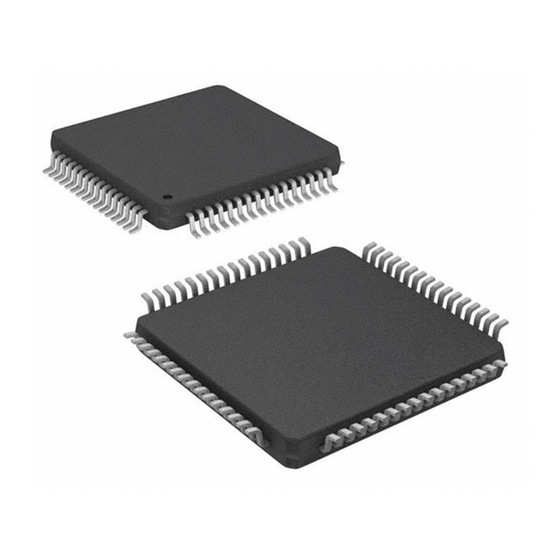
Page 48: Pinout And Pin Functions
XMEGA A3 29. Pinout and Pin Functions The pinout of XMEGA A3 is shown in ”Pinout/Block Diagram” on page 2. In addition to general I/O functionality, each pin may have several function. This will depend on which peripheral is enabled and connected to the actual pin. Only one of the alternate pin functions can be used at time. - Page 49 XMEGA A3 29.1.4 Timer/Counter and AWEX functions OCnx Output Compare Channel x for Timer/Counter n OCxn Inverted Output Compare Channel x for Timer/Counter n 29.1.5 Communication functions Serial Clock for TWI Serial Data for TWI SCLIN Serial Clock In for TWI when external driver interface is enabled SCLOUT Serial Clock Out for TWI when external driver interface is enabled SDAIN...
-
Page 50: Alternate Pin Functions
XMEGA A3 29.2 Alternate Pin Functions The tables below show the main and alternate pin functions for all pins on each port. They also show which peripheral that makes use of or enables the alternate pin function. Table 29-1. Port A - Alternate functions ADAA ADCA PORT A... - Page 51 XMEGA A3 Table 29-3. Port C - Alternate functions PORT C PIN # INTERRUPT TCC0 AWEXC TCC1 USARTC0 USARTC1 SPIC TWIC CLOCKOUT EVENTOUT SYNC OC0A OC0A SYNC OC0B OC0A XCK0 SYNC/ASYNC OC0C OC0B RXD0 SYNC OC0D OC0B TXD0 SYNC OC0C OC1A SYNC OC0C...
- Page 52 XMEGA A3 Table 29-6. Port F - Alternate functions PORT F PIN # INTERRUPT TCF0 USARTF0 SYNC OC0A SYNC OC0B XCK0 SYNC/ASYNC OC0C RXD0 SYNC OC0D TXD0 SYNC SYNC SYNC SYNC Table 29-7. Port R - Alternate functions PORT R PIN # INTERRUPT PROGR...
-
Page 53: Peripheral Module Address Map
XMEGA A3 30. Peripheral Module Address Map The address maps show the base address for each peripheral and module in XMEGA A3. For complete register description and summary for each peripheral module, refer to the XMEGA A Manual. Base Address Name Description 0x0000... -
Page 54: Instruction Set Summary
XMEGA A3 31. Instruction Set Summary Mnemonics Operands Description Operation Flags #Clocks Arithmetic and Logic Instructions ← Rd, Rr Add without Carry Rd + Rr Z,C,N,V,S,H ← Rd, Rr Add with Carry Rd + Rr + C Z,C,N,V,S,H ← ADIW Rd, K Add Immediate to Word Rd + 1:Rd + K... - Page 55 XMEGA A3 Mnemonics Operands Description Operation Flags #Clocks ← CALL call Subroutine None 3 / 4 ← Subroutine Return STACK None 4 / 5 ← RETI Interrupt Return STACK 4 / 5 ← CPSE Rd,Rr Compare, Skip if Equal if (Rd = Rr) PC PC + 2 or 3 None 1 / 2 / 3...
- Page 56 XMEGA A3 Mnemonics Operands Description Operation Flags #Clocks ← (1)(2) Rd, -Y Load Indirect and Pre-Decrement Y - 1 None ← ← (1)(2) Rd, Y+q Load Indirect with Displacement (Y + q) None ← (1)(2) Rd, Z Load Indirect None ←...
- Page 57 XMEGA A3 Mnemonics Operands Description Operation Flags #Clocks ← Rotate Left Through Carry Rd(0) Z,C,N,V,H ← Rd(n+1) Rd(n), ← Rd(7) ← Rotate Right Through Carry Rd(7) Z,C,N,V ← Rd(n) Rd(n+1), ← Rd(0) ← Arithmetic Shift Right Rd(n) Rd(n+1), n=0..6 Z,C,N,V ↔...
-
Page 58: Electrical Characteristics - Tbd
XMEGA A3 32. Electrical Characteristics - TBD 32.1 Absolute Maximum Ratings* *NOTICE: Stresses beyond those listed under “Absolute Operating Temperature........-55°C to +125°C Maximum Ratings” may cause permanent dam- age to the device. This is a stress rating only and Storage Temperature ........ -
Page 59: Speed
XMEGA A3 32.3 Speed The maximum frequency of the XMEGA A3 devices is depending on VCC. As shown in Figure 32-1 on page 59 the Frequency vs. VCC curve is linear between 1.8V < VCC < 2.7V. Figure 32-1. Maximum Frequency vs. Vcc Safe Operating Area 8068C–AVR–06/08... -
Page 60: Adc Characteristics - Tbd
XMEGA A3 32.4 ADC Characteristics – TBD Table 32-1. ADC Characteristics Symbol Parameter Condition Units Resolution Integral Non-Linearity (INL) Differential Non-Linearity (DNL) Gain Error Offset Error Conversion Time µs ADC Clock Frequency DC Supply Voltage Ω Source Impedance Start-up time µs AVCC Analog Supply Voltage... -
Page 61: Dac Characteristics - Tbd
XMEGA A3 32.5 DAC Characteristics – TBD Table 32-3. DAC Characteristics Symbol Parameter Condition Units Resolution Integral Non-Linearity (INL) Differential Non-Linearity (DNL) Gain Error Offset Error Calibrated Gain/Offset Error Output Range Output Settling Time µs Output Capacitance Output Resistance kΩ Reference Input Voltage Reference Input Capacitance Reference Input Resistance... -
Page 62: Typical Characteristics - Tbd
XMEGA A3 33. Typical Characteristics - TBD 8068C–AVR–06/08... -
Page 63: Packaging Information
XMEGA A3 34. Packaging information 34.1 PIN 1 PIN 1 IDENTIFIER 0°~7° COMMON DIMENSIONS (Unit of Measure = mm) NOTE SYMBOL – – 1.20 0.05 – 0.15 0.95 1.00 1.05 15.75 16.00 16.25 13.90 14.00 14.10 Note 2 15.75 16.00 16.25 Notes: 13.90... -
Page 64: 4M1
XMEGA A3 34.2 64M1 Marked Pin# 1 ID SEATING PLANE TOP VIEW 0.08 Pin #1 Corner SIDE VIEW Pin #1 Option A Triangle COMMON DIMENSIONS (Unit of Measure = mm) SYMBOL NOTE Option B 0.80 0.90 1.00 Pin #1 Chamfer –... -
Page 65: Errata
XMEGA A3 35. Errata 35.1 All rev. No known errata. 8068C–AVR–06/08... -
Page 66: Datasheet Revision History
XMEGA A3 36. Datasheet Revision History 36.1 8068C – 06/08 Updated ”Features” on page Updated Figure 2-1 on page Updated ”Overview” on page Updated Table 7-2 on page Replaced Figure 24-1 on page 41 by a correct one. Updated “Features” ”Overview”... -
Page 67: Table Of Contents
XMEGA A3 Table of Contents Features ..................... 1 Typical Applications ................1 Ordering Information ................2 Pinout/Block Diagram ................2 Overview ....................3 3.1Block Diagram ......................4 Resources ....................5 4.1Recommended reading .....................5 Disclaimer ....................5 AVR CPU ....................6 6.1Features ........................6 6.2Overview ........................6 6.3Register File ......................7 6.4ALU - Arithmetic Logic Unit ..................7... - Page 68 XMEGA A3 10.2Overview ........................17 10.3Clock Options ......................18 11 Power Management and Sleep Modes ..........20 11.1Features ........................20 11.2Overview ........................20 11.3Sleep Modes ......................20 12 System Control and Reset ..............22 12.1Features ........................22 12.2Resetting the AVR ....................22 12.3Reset Sources .......................22 12.4WDT - Watchdog Timer ..................23 13 PMIC - Programmable Multi-level Interrupt Controller .......
- Page 69 XMEGA A3 18.2Overview ........................34 19 TWI - Two Wire Interface ............... 35 19.1Features ........................35 19.2Overview ........................35 20 SPI - Serial Peripheral Interface ............36 20.1Features ........................36 20.2Overview ........................36 21 USART ..................... 37 21.1Features ........................37 21.2Overview ........................37 22 IRCOM - IR Communication Module ............. 38 22.1Features ........................38 22.2Overview ........................38 23 Crypto Engine ..................
- Page 70 XMEGA A3 28.3JTAG interface .......................47 28.4PDI - Program and Debug Interface ..............47 29 Pinout and Pin Functions ..............48 29.1Alternate Pin Function Description ................48 29.2Alternate Pin Functions ..................50 30 Peripheral Module Address Map ............53 31 Instruction Set Summary ............... 54 32 Electrical Characteristics - TBD ............
- Page 71 Disclaimer: The information in this document is provided in connection with Atmel products. No license, express or implied, by estoppel or otherwise, to any intellectual property right is granted by this document or in connection with the sale of Atmel products. EXCEPT AS SET FORTH IN ATMEL’S TERMS AND CONDI- TIONS OF SALE LOCATED ON ATMEL’S WEB SITE, ATMEL ASSUMES NO LIABILITY WHATSOEVER AND DISCLAIMS ANY EXPRESS, IMPLIED OR STATUTORY...
Need help?
Do you have a question about the XMEGA A3 series and is the answer not in the manual?
Questions and answers