Table of Contents
Advertisement
Quick Links
Advertisement
Table of Contents

Related Manuals for Aaeon PICO-BSW1


Summary of Contents for Aaeon PICO-BSW1
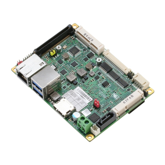
- Page 1 PICO-BSW1 Pico-ITX Board User’s Manual 3 Last Updated: May 18, 2017...
- Page 2 AAEON assumes no liabilities resulting from errors or omissions in this document, or from the use of the information contained herein. AAEON reserves the right to make changes in the product design without notice to its users.
- Page 3 Acknowledgement All other products’ name or trademarks are properties of their respective owners. Microsoft Windows ® is a registered trademark of Microsoft Corp. ITE is a trademark of Integrated Technology Express, Inc. IBM, PC/AT, PS/2, and VGA are trademarks of International Business Machines ...
- Page 4 Packing List Before setting up your product, please make sure the following items have been shipped: Item Quantity PICO-BSW1 Product DVD with User’s Manual (in pdf) and drivers Heat Spreader COM + Line-out Cable If any of these items are missing or damaged, please contact your distributor or sales representative immediately.
- Page 5 (if any), its specifications, dimensions, jumper/connector settings/definitions, and driver installation instructions (if any), to facilitate users in setting up their product. Users may refer to the AAEON.com for the latest version of this document. Preface...
- Page 6 Safety Precautions Please read the following safety instructions carefully. It is advised that you keep this manual for future references All cautions and warnings on the device should be noted. Make sure the power source matches the power rating of the device. Position the power cord so that people cannot step on it.
- Page 7 If any of the following situations arises, please the contact our service personnel: Damaged power cord or plug Liquid intrusion to the device iii. Exposure to moisture Device is not working as expected or in a manner as described in this manual The device is dropped or damaged Any obvious signs of damage displayed on the device...
- Page 8 FCC Statement This device complies with Part 15 FCC Rules. Operation is subject to the following two conditions: (1) this device may not cause harmful interference, and (2) this device must accept any interference received including interference that may cause undesired operation.
- Page 9 China RoHS Requirements (CN) 产品中有毒有害物质或元素名称及含量 AAEON Main Board/ Daughter Board/ Backplane 有毒有害物质或元素 部件名称 铅 汞 镉 六价铬 多溴联苯 多溴二苯醚 (Pb) (Hg) (Cd) (Cr(VI)) (PBB) (PBDE) 印刷电路板 ○ ○ ○ ○ ○ ○ 及其电子组件 外部信号 ○ ○ ○ ○ ○ ○...
- Page 10 China RoHS Requirement (EN) Poisonous or Hazardous Substances or Elements in Products AAEON Main Board/ Daughter Board/ Backplane Poisonous or Hazardous Substances or Elements Hexavalent Polybrominated Polybrominated Component Lead Mercury Cadmium Chromium Biphenyls Diphenyl Ethers (Pb) (Hg) (Cd) (Cr(VI)) (PBB) (PBDE) PCB &...
-
Page 11: Table Of Contents
Table of Contents Chapter 1 - Product Specifications..................1 Specifications ......................2 Chapter 2 – Hardware Information ..................4 Dimensions ....................... 5 Jumpers and Connectors ..................9 List of Jumpers ......................11 2.3.1 Auto Power Button and Clear CMOS Jumper (JP1) ......12 2.3.2 LVDS Port VDD and Backlight Inverter VCC Selection (JP2) ... - Page 12 2.4.16 HDMI Port (CN24) ..................31 Chapter 3 - AMI BIOS Setup ....................33 System Test and Initialization ................34 AMI BIOS Setup ..................... 35 Setup Submenu: Main ..................36 Setup Submenu: Advanced ................. 37 3.4.1 Advanced: CPU configuration ..............39 3.4.2 Advanced: SATA Configuration .............41 3.4.3...
- Page 13 Appendix B - I/O Information ....................70 I/O Address Map ....................71 Memory Address Map ..................74 IRQ Mapping Chart ....................76 Appendix C – Electrical Specifications for I/O Ports ............88 Electrical Specifications for I/O Ports ..............89 Appendix D – Mating Connectors ..................90 List of Mating Connectors and Cables ...............
-
Page 14: Chapter 1 - Product Specifications
Chapter 1 Chapter 1 - Product Specifications... -
Page 15: Specifications
Specifications System Pico-ITX Form Factor Intel® N3160 Quad Core 1.6GHz (6W), Processor Intel® N3060 Dual Core 1.6GHz (6W), Intel® X5-E8000 Quad Core 1.04GHz (5W) 204-pin DDR3L 1600 SODIMM, up to 8 GB System Memory Intel® N3160 Quad Core 1.6GHz (6W), Chipset ... - Page 16 Display Intel® N3160 Quad Core 1.6GHz (6W), Chipset Intel® N3060 Dual Core 1.6GHz (6W), Intel® X5-E8000 Quad Core 1.04GHz (5W) LVDS (18/24bit 2CH) 1920 x 1200 Resolution HDMI up to 3840 x 2160 DDI (BIO) LCD Interface 18/24-bit LVDS ...
-
Page 17: Chapter 2 - Hardware Information
Chapter 2 Chapter 2 – Hardware Information... -
Page 18: Dimensions
Dimensions Component Side Component Side Chapter 2 – Hardware Information... - Page 19 Solder Side Solder Side Chapter 2 – Hardware Information...
- Page 20 Heat Spreader Chapter 2 – Hardware Information...
- Page 21 Chapter 2 – Hardware Information...
-
Page 22: Jumpers And Connectors
Jumpers and Connectors Component Side Component Side Component Side Chapter 2 – Hardware Information... - Page 23 Solder Side Chapter 2 – Hardware Information...
-
Page 24: List Of Jumpers
List of Jumpers Please refer to the table below for all of the board’s jumpers that you can configure for your application Label Function Auto Power Button Selection and Clear CMOS Jumper LVDS Port VDD and Backlight Inverter VCC Selection LVDS Port Backlight Lightness Control Mode Selection COM2 Pin8 Function Selection Chapter 2 –... -
Page 25: Auto Power Button And Clear Cmos Jumper (Jp1)
2.3.1 Auto Power Button and Clear CMOS Jumper (JP1) CMOS Normal (Default) (1-3) Clear CMOS (3-5) AT Mode (2-4) ATX Mode (4-6) 2.3.2 LVDS Port VDD and Backlight Inverter VCC Selection (JP2) LVDS Port VDD +3.3V (Default) (3-5) LVDS Port VDD +5V (1-3) Backlight Inverter VCC +5V (Default) Backlight Inverter VCC +12V (4-6) (2-4) -
Page 26: List Of Connectors
List of Connectors Please refer to the table below for all of the board’s connectors that you can configure for your application Label Function JP16 Front Panel Connector USB Ports 0 and 1 RTC Battery LVDS Port Inverter / Backlight Connector LVDS Port BIO (Board-Board Connector) LAN (RJ-45) -
Page 27: Front Panel Connector (Jp16)
2.4.1 Front Panel Connector (JP16) Pin Name Pin Name Pin 1 PWR_BTN- Pin 2 PWR_BTN+ Pin 3 HDD_LED- Pin 4 HDD_LED+ Pin 5 SPEAKER- Pin 6 SPEAKER+ Pin 7 PWR_LED- Pin 8 PWR_LED+ Pin 9 H/W RESET- Pin 10 H/W RESET+ 2.4.2 USB Ports 0 and 1 (CN1) Pin Name Signal Type... -
Page 28: Rtc Battery (Cn3)
Pin Name Signal Type Signal level USB0_SSRX− DIFF USB0_SSRX+ DIFF USB0_SSTX− DIFF USB0_SSTX+ DIFF +5VSB USB1_D- DIFF USB1_D+ DIFF USB1_SSRX− USB1_SSRX+ USB1_SSTX− USB1_SSTX+ 2.4.3 RTC Battery (CN3) Pin Name Signal Type Signal level +3.3V 3.3V Chapter 2 – Hardware Information... -
Page 29: Lvds Port Inverter / Backlight Connector (Cn5)
2.4.4 LVDS Port Inverter / Backlight Connector (CN5) BLK_PWR BKL_CONTROL BKL_ENABLE Pin Name Signal Type Signal Level BKL_PWR +5V / +12V BKL_CONTROL BKL_ENABLE +3.3V 2.4.5 LVDS Port (CN6) Pin Name Signal Type Signal Level BKL_ENABLE BKL_CONTROL LCD_PWR +3.3V/+5V Chapter 2 – Hardware Information... - Page 30 Pin Name Signal Type Signal Level LVDS_A_CLK- DIFF LVDS_A_CLK+ DIFF LCD_PWR +3.3V/+5V LVDS_DA0- DIFF LVDS_DA0+ DIFF LVDS_DA1- DIFF LVDS_DA1+ DIFF LVDS_DA2- DIFF LVDS_DA2+ DIFF LVDS_DA3- DIFF LVDS_DA3+ DIFF DDC_DATA +3.3V DDC_CLK +3.3V LVDS_DB0- DIFF LVDS_DB0+ DIFF LVDS_DB1- DIFF LVDS_DB1+ DIFF LVDS_DB2- DIFF Chapter 2 –...
-
Page 31: Bio Connector (Cn8)
Pin Name Signal Type Signal Level LVDS_DB2+ DIFF LVDS_DB3- DIFF LVDS_DB3+ DIFF LCD_PWR +3.3V/+5V LVDS_B_CLK- DIFF LVDS_B_CLK+ DIFF 2.4.6 BIO Connector (CN8) Pin Name Pin Name +12VSB PCIE_TXN0 PCIE_RXN0 PCIE_TXP0 PCIE_RXP0 PS_ON# +5VSB +5VSB +5VSB +5VSB PCIE_REF_CLK0 RESET# PCIE_REF_CLK0# Chapter 2 – Hardware Information... - Page 32 Pin Name Pin Name USBN0 USBP0 USBN1 USBP2 SMB_CLK SMB_DATA WAKE# USB_OC0# USB_OC1# LPC_AD0 LPC_FRAME# LPC_AD1 SERIRQ LPC_AD2 LPC_DRQ LPC_AD3 PWG/GPIO0 AGND LPC_CLK AUD_LINEOUT_L PME# AUD_LINEOUT_R Chapter 2 – Hardware Information...
-
Page 33: Lan (Rj-45) Port (Cn9)
Pin Name Pin Name 2.4.7 LAN (RJ-45) Port (CN9) Pin Name Signal Type Signal Level MDI0+ DIFF MDI0- DIFF MDI1+ DIFF MDI2+ DIFF MDI2- DIFF MDI1- DIFF MDI3+ DIFF MDI3- DIFF 2.4.8 Mini-Card Slot (Half-Mini Card) (CN10) Pin Name Signal Type Signal Level PCIE_WAKE# +3.3VSB... - Page 34 Pin Name Signal Type Signal Level +1.5V +1.5V PCIE_CLK_REQ# PCIE_REF_CLK- DIFF PCIE_REF_CLK+ DIFF W_DISABLE# +3.3V PCIE_RST# +3.3V PCIE_RX- DIFF +3.3VSB +3.3V Chapter 2 – Hardware Information...
- Page 35 Pin Name Signal Type Signal Level PCIE_RX+ DIFF +1.5V +1.5V SMB_CLK +3.3V PCIE_TX- DIFF SMB_DATA +3.3V PCIE_TX+ DIFF USB_D- DIFF USB_D+ DIFF +3.3VSB +3.3V +3.3VSB +3.3V Chapter 2 – Hardware Information...
-
Page 36: Sata Port (Cn11)
Pin Name Signal Type Signal Level +1.5V +1.5V +3.3VSB +3.3V 2.4.9 SATA Port (CN11) Pin Name Signal Type Signal Level SATA_TX1+ DIFF SATA_TX1- DIFF SATA_RX1- DIFF SATA_RX1+ DIFF Chapter 2 – Hardware Information... -
Page 37: Output For Sata Hdd (Cn12)
2.4.10 +5V Output for SATA HDD (CN12) Pin Name Signal Type Signal Level 2.4.11 MiniCard Slot (Full-Mini Card) (CN13) Pin Name Signal Type Signal level PCIE_WAKE# +3.3V +3.3VSB/+3.3V +1.5V +1.5V PCIE_CLK_REQ# UIM_PWR UIM_DATA PCIE_REF_CLK- DIFF Chapter 2 – Hardware Information... - Page 38 Pin Name Signal Type Signal level UIM_CLK PCIE_REF_CLK+ DIFF UIM_RST UIM_VPP W_DISABLE# +3.3V PCIE_RST# +3.3V PCIE_RX-/mSATARX+ DIFF +3.3VSB/+3.3V +3.3V PCIE_RX+/mSATARX- DIFF +1.5V +1.5V SMB_CLK +3.3V PCIE_TX-/mSATATX- DIFF SMB_DATA +3.3V Chapter 2 – Hardware Information...
-
Page 39: Digital Io Port (Cn18)
Pin Name Signal Type Signal level PCIE_TX+/mSATATX+ DIFF USB_D- DIFF USB_D+ DIFF +3.3VSB/+3.3V +3.3V +3.3VSB/+3.3V +3.3V +1.5V +1.5V +3.3VSB/+3.3V +3.3V 2.4.12 Digital IO Port (CN18) Chapter 2 – Hardware Information... -
Page 40: Lpc Port (Cn20)
Pin Name Signal Type Signal Level DIO0 DIO1 DIO2 DIO3 2.4.13 LPC Port (CN20) Pin Name Signal Type Signal Level +3.3V LAD0 +3.3V LAD1 +3.3V LAD2 Chapter 2 – Hardware Information... - Page 41 Pin Name Signal Type Signal Level +3.3V LAD3 +3.3V +3.3V LFRAME# +3.3V LRESET# LCLK I2C0_CLK +3.3V (Default)/SMBUS_CLK(Option) I2C_DATA (Default) +3.3V /SMBUS_DATA(Option) +3.3V SERIRQ SMBUS (Optional) Pin Name Signal Type Signal Level +3.3V SMBUS_CLK +3.3V SMBUS_DATA Chapter 2 – Hardware Information...
-
Page 42: Com Port & Audio I/O Connector (Cn21)
I2C (Optional) Pin Name Signal Type Signal Level +3.3V I2C0_CLK +3.3V I2C0_DATA 2.4.14 COM Port & Audio I/O Connector (CN21) Pin Name Signal Type Signal Level DCDB DSRB RTSB ±9V ±9V Chapter 2 – Hardware Information... - Page 43 Pin Name Signal Type Signal Level CTSB DTRB ±9V RIB/+5V/+12V IN/ PWR +5V/+12V DCDA DSRA RTSA ±9V ±9V CTSA DTRA ±9V AGND LOUT_R LOUT_L Chapter 2 – Hardware Information...
-
Page 44: External +12V Input (Cn22)
2.4.15 External +12V Input (CN22) Pin Name Signal Type Signal Level +12V +12V 2.4.16 HDMI Port (CN24) Pin Name Signal Type Signal Level TMDS_DAT2+ DIFF TMDS_DAT2- DIFF TMDS_DAT1+ DIFF TMDS_DAT1- DIFF TMDS_DAT0+ DIFF TMDS_DAT0- DIFF TMDS_CLK+ DIFF Chapter 2 – Hardware Information... - Page 45 Pin Name Signal Type Signal Level TMDS_CLK- DIFF DDC_CLK DDC_DATA HPLG_DETECT Chapter 2 – Hardware Information...
-
Page 46: Chapter 3 - Ami Bios Setup
Chapter 3 Chapter 3 - AMI BIOS Setup... -
Page 47: System Test And Initialization
System Test and Initialization The board uses certain routines to perform testing and initialization. If an error, fatal or non-fatal, is encountered, a few short beeps or an error message will be outputted. The board can usually continue the boot up sequence with non-fatal errors. The system configuration verification routines check the current system configuration against the values stored in the CMOS memory. -
Page 48: Ami Bios Setup
AMI BIOS Setup The AMI BIOS ROM has a pre-installed Setup program that allows users to modify basic system configurations, which is stored in the battery-backed CMOS RAM and BIOS NVRAM so that the information is retained when the power is turned off. To enter BIOS Setup, press <Del>... -
Page 49: Setup Submenu: Main
Setup Submenu: Main Press “Delete” to enter Setup Options summary: (default setting) System Date Day MM:DD:YYYY Change the month, year and century. The ‘Day’ is changed automatically. System Time HH : MM : SS Change the clock of the system. Chapter 3 –... -
Page 50: Setup Submenu: Advanced
Setup Submenu: Advanced Options summary: (default setting) CPU Configuration CPU Configuration Parameters SATA Configuration SATA Device Configuration USB Configuration USB Configuration Parameters SIO Configuration SIO Chip configuration .Enable or Disable SIO Logical Devices, Resources and Features settings, etc. Hardware Monitor Chapter 3 –... - Page 51 Power Management System ACPI/Power Mode/Wake Event Configuration Digital IO Port Configuration Set Input/Output of digital Port Configuration Chapter 3 – AMI BIOS Setup...
-
Page 52: Advanced: Cpu Configuration
3.4.1 Advanced: CPU configuration Options summary: (default setting) EIST Enabled Disabled Enable/Disable Intel SpeedStep feature. Turbo Mode Enabled Disabled Turbo mode. Chapter 3 – AMI BIOS Setup... - Page 53 Intel Virtualization Enabled Technology Disabled When enabled, a VMM can utilize the additional hardware capabilities provide by Vanderpool Technology CPU C state Report Enabled Disabled Enable/Disable CPU C state report to OS. Chapter 3 – AMI BIOS Setup...
-
Page 54: Advanced: Sata Configuration
3.4.2 Advanced: SATA Configuration Options summary: (default setting) SATA Mode AHCI Mode Only AHCI mode support on this platform SATA Port0/Port1 Enabled HotPlug Disabled Enabled/Disabled SATA Port0/Port1 HotPlug function Chapter 3 – AMI BIOS Setup... -
Page 55: Advanced: Usb Configuration
3.4.3 Advanced: USB Configuration Options summary: (default setting) XHCI Mode Enabled Disabled Mode of operation of xHCI controller Legacy USB Support Enabled Disabled Auto Enables BIOS Support for Legacy USB Support. When enabled, USB can be functional in legacy environment like DOS. AUTO option disables legacy support if no USB devices are connected. -
Page 56: Advanced: Sio Configuration
3.4.4 Advanced: SIO Configuration Options summary: (default setting) Serial Port 1/2 Configuration View and Set Basic properties of the SIO Logical device. Like IO Base , IRQ Range , DMA Channel and Device Mode. Chapter 3 – AMI BIOS Setup... -
Page 57: Sio Configuration: Serial Port 1 / 2 Configuration
3.4.4.1 SIO Configuration: Serial Port 1 / 2 Configuration Options summary: (default setting) Use This Device Disabled Enabled En/Disable specified serial port. Change Settings Use Automatic Settings (COM1) IO=3F8h; IRQ=4; IO=2F8h; IRQ=3; Change Settings Use Automatic Settings (COM2) IO=2F8h; IRQ=3; IO=3F8h;... - Page 58 RS422 RS485 Configure COM operated as RS232, RS422 or RS485. Only COM2 support this function. Chapter 3 – AMI BIOS Setup...
-
Page 59: Advanced: Hardware Monitor
3.4.5 Advanced: Hardware Monitor Chapter 3 – AMI BIOS Setup... -
Page 60: Advanced: Csm Configuration
3.4.6 Advanced: CSM Configuration Options summary: (default setting) Enabled CSM Support Disable Enable/Disable CSM Support. UEFI and Legacy Boot option filter Legacy only UEFI only This option controls Legacy/UEFI ROMs priority DIsabled Launch PXE ROM Enabled Controls the execution of UEF and Legacy PXE OpROM Chapter 3 –... - Page 61 Do not launch Storage UEFI Legacy Controls the execution of UEFI and Legacy Storage OpROM. Do not launch Video UEFI Legacy Controls the execution of UEFI and Legacy Video OpROM. Chapter 3 – AMI BIOS Setup...
-
Page 62: Advanced: Power Management
3.4.7 Advanced: Power Management Options summary: (default setting) ATX Type Power Mode AT Type Select system power mode Power Off Restore AC Power Loss Power on Late State Enabled RI Wake Event Disabled Enabled or disabled wake on ring function. Chapter 3 –... - Page 63 RTC wake system from Disabled Fixed Time Dynamic Time Enable system to wake from S5 using RTC alarm. Wake up day 0-31 Select 0 for daily system wake up 1-31 for which day of the month that you would like the system to wake up Wake up hour 0-23 Wake up minute...
-
Page 64: Advanced: Digital Io Port Configuration
3.4.8 Advanced: Digital IO Port Configuration Options summary: (default setting) DIO Port1/2/3/4 Input Output Set DIO Port1/2/3/4 as Input or Output DIO Port5/6/7/8 Input Output Set GPIO3/GPIO4 as Input or Output Output Level Set GPIO Level when used as Output Chapter 3 –... -
Page 65: Setup Submenu: Chipset
Setup submenu: Chipset Options summary: (default setting) North Bridge North Bridge Parameters. South Bridge South Bridge Parameters Chapter 3 – AMI BIOS Setup... -
Page 66: Chipset: North Bridge
3.5.1 Chipset: North Bridge Options summary: (default setting) Max TOLUD 2.25 GB 2.5 GB 2.75 GB Maximum Value of TOLUD. Chapter 3 – AMI BIOS Setup... - Page 67 Primary Boot Display Auto Extension Board LVDS HDMI Select the Video Device which will be activated during POST. This has no effect if external graphics present. Secondary boot display Selection will appear based on your selection. VGA mode will be supported only on primary disply. Secondary Boot Display Disabled Extension Board LVDS...
-
Page 68: North Bridge: Lvds Panel Configuration
3.5.1.1 North Bridge: LVDS Panel Configuration Options summary: (default setting) LVDS Disabled Enabled Enable or Disable LVDS interface Panel Type 640x480 800x480 800x600 1024x600 1024x768 1280x768 1280x800 1280x1024 1366x768 Chapter 3 – AMI BIOS Setup... - Page 69 1440x900 1600x1200 1920x1080 1920x1200 Select panel resolution. Color Depth 18-Bit 24-Bit 36-Bit 48-Bit Select color depth of the panel Backlight Type Inverted Normal Select Backlight control type. Inverted: Brightest for low PWM duty cycle and low voltage. Normal: Brightest for high PWM duty cycle and high voltage. Backlight Level 100% Select Backlight Level...
-
Page 70: Chipset: South Bridge
3.5.2 Chipset: South Bridge Options summary: (default setting) Audio Controller Disabled Enabled Enable or disabled Azalia device for audio function. Chapter 3 – AMI BIOS Setup... -
Page 71: Setup Submenu: Security
Setup submenu: Security Change User/Administrator Password You can set a User Password once an Administrator Password is set. The password will be required during boot up, or when the user enters the Setup utility. Please Note that a User Password does not provide access to many of the features in the Setup utility. -
Page 72: Setup Submenu: Boot
Setup submenu: Boot Options summary: (default setting) Quiet Boot Disabled Enabled En/Disable showing boot logo. Launch PXE OpROM Disabled Enabled En/Disable network OpROM for legacy PXE boot Boot Option #X/ XXXX Drive BBS Priorities The order of boot priorities. Chapter 3 – AMI BIOS Setup... -
Page 73: Boot: Bbs Priorities
3.7.1 Boot: BBS Priorities Options summary: (default setting) Boot Option #x Disabled Device name Sets the system boot order Chapter 3 – AMI BIOS Setup... -
Page 74: Setup Submenu: Save & Exit
Setup submenu: Save & Exit Options summary: (default setting) Save Changes and Reset Reset the system after saving the changes Discard Changes and Exit Reset system setup without saving any changes Restore Defaults Restore/Load Default values for all the setup options. Chapter 3 –... -
Page 75: Chapter 4 - Drivers Installation
Chapter 4 Chapter 4 – Drivers Installation... -
Page 76: Product Cd/Dvd
Product CD/DVD The PICO-BSW1 comes with a product DVD that contains all the drivers and utilities you need to setup your product. Insert the DVD and follow the steps in the autorun program to install the drivers. In case the program does not start, follow the sequence below to install the drivers. - Page 77 Step 4 – Install Audio Driver Open the Step4 - Audio folder and select your OS Open the Setup.exe file in the folder Follow the instructions Driver will be installed automatically Step 5 – Install TXE Driver Open the Step5 - TXE folder and open the Setup.exe file Follow the instructions Driver will be installed automatically Step 6 –...
-
Page 78: Appendix A - Watchdog Timer Programming
Appendix A Appendix A - Watchdog Timer Programming... -
Page 79: Watchdog Timer Registers
Watchdog Timer Registers Table 1 : Watch dog relative IO address Default Value Note I/O Base I/O Base address for Watchdog operation. 0x2E Address This address is assigned by SIO LDN7 Table 2 : Watchdog relative register table Register Offset BitNum Value Note... -
Page 80: Watchdog Sample Program
A.2 Watchdog Sample Program ****************************************************************************** // WDT I/O operation relative definition (Please reference to Table 1) #define WDTAddr 0x510 // WDT I/O base address Void WDTWriteByte(byte Register, byte Value); byte WDTReadByte(byte Register); Void WDTSetReg(byte Register, byte Bit, byte Val); // Watch Dog relative definition (Please reference to Table 2) #define DevReg 0x00 // Device configuration register #define WDTRstBit 0x80 // Watchdog WDTRST# (Bit7) - Page 81 ******************************************************************************* // Procedure : AaeonWDTEnable VOID EnterSIOconfig IOWriteByte (IoConfAddr,0x87); IOWriteByte (IoConfAddr,0x87); VOID ExitSIOconfig IOWriteByte (IoConfAddr,0xAA); VOID SetWDT IOWriteByte (IoConfAddr,0x2B); IOWriteByte(IoConfAddr+1, (IOReadByte(IoConfAddr+1)&0xFC)); // Procedure : AaeonWDTEnable AaeonWDTEnable () VOID WDTEnableDisable(1); // Procedure : AaeonWDTConfig AaeonWDTConfig (byte Counter, BOOLEAN Unit) VOID // Disable WDT counting WDTEnableDisable( // Clear Watchdog Timeout Status WDTClearTimeoutStatus();...
- Page 82 WDTSetBit( TimerReg, UnitBit, Unit // WDT output mode set to pulse WDTSetBit( TimerReg, ModeBit, ModeVal // WDT output mode set to active low WDTSetBit( TimerReg, PolarityBit, PolarityVal // WDT output pulse width is 25ms WDTSetBit( TimerReg, PSWidthBit, PSWidthVal // Watchdog WDTRST# Enable WDTSetBit( DevReg, WDTRstBit, WDTRstVal WDTClearTimeoutStatus()
-
Page 83: Appendix B - I/O Information
Appendix B Appendix B - I/O Information... -
Page 84: I/O Address Map
I/O Address Map Appendix B – I/O Information... - Page 85 Appendix B – I/O Information...
- Page 86 Appendix B – I/O Information...
-
Page 87: Memory Address Map
Memory Address Map Appendix B – I/O Information... - Page 88 Appendix B – I/O Information...
-
Page 89: Irq Mapping Chart
IRQ Mapping Chart Appendix B – I/O Information... - Page 90 Appendix B – I/O Information...
- Page 91 Appendix B – I/O Information...
- Page 92 Appendix B – I/O Information...
- Page 93 Appendix B – I/O Information...
- Page 94 Appendix B – I/O Information...
- Page 95 Appendix B – I/O Information...
- Page 96 Appendix B – I/O Information...
- Page 97 Appendix B – I/O Information...
- Page 98 Appendix B – I/O Information...
- Page 99 Appendix B – I/O Information...
- Page 100 Appendix B – I/O Information...
-
Page 101: Appendix C - Electrical Specifications For I/O Ports
Appendix C Appendix C – Electrical Specifications for I/O Ports... -
Page 102: Electrical Specifications For I/O Ports
Electrical Specifications for I/O Ports Reference Signal Name Rate Output +5VSB/1A (per USB 3.0 Ports 0 & 1 +5VSB channel) LVDS Port Inverter / +5V/2A or Backlight Connector +12V/2A +3.3V/2A or LVDS Port +5V/2A MiniCard Slot +3.3VSB +3.3V/1.1A CN10 (Halfl MiniCard) +1.5V +1.5V/0.375A +5V Output for... -
Page 103: Appendix D - Mating Connectors
Appendix D Appendix D – Mating Connectors... -
Page 104: List Of Mating Connectors And Cables
CN13 Mini-Card FOXCONN AS0B226-S68Q- Slot (Full-Mini Card) CN18 Digital IO SM6B-GHS-TB Port CN20 LPC Port SHR-12V-S-B AAEON LPC 1703120130 Cable CN21 COM Port DF14-20S-1.25C COM Port 1703200153 1/2 & line 1/2 & line out cable connector Appendix D –Mating Connectors... - Page 105 CN22 External DINKLE DT-126VP-S2016 Power cable 170204010R +12V Input 002P DIMM1 DDR3 FOXCONN AS0A626-JER6-7 204PIN SKT JP16 Buzzer PINREX 712-73-02TWE0 Buzzer 170302010C connector Cable JP16 Front Panel PINREX 222-97-05GBE1 Front 1701100156 Connector Panel Cable Appendix D –Mating Connectors...
Need help?
Do you have a question about the PICO-BSW1 and is the answer not in the manual?
Questions and answers