Chapters
Table of Contents
Troubleshooting

Subscribe to Our Youtube Channel
Related Manuals for Omron CS1W-AD041-V1


Summary of Contents for Omron CS1W-AD041-V1
- Page 1 Cat. No. W345-E1-08 SYSMAC CS/CJ Series CS1W-AD041-V1/AD081-V1/AD161 CS1W-DA041/DA08V/DA08C CS1W-MAD44 CJ1W-AD041-V1/AD081-V1 CJ1W-DA021/DA041/DA08V/DA08C CJ1W-MAD42 Analog I/O Units OPERATION MANUAL...
- Page 2 SYSMAC CS/CJ Series CS1W-AD041-V1/AD081-V1/AD161 CS1W-DA041/DA08V/DA08C CS1W-MAD44 CJ1W-AD041-V1/AD081-V1 CJ1W-DA021/DA041/DA08V/DA08C CJ1W-MAD42 Analog I/O Units Operation Manual Revised July 2005...
- Page 4 OMRON. No patent liability is assumed with respect to the use of the information contained herein. Moreover, because OMRON is con- stantly striving to improve its high-quality products, the information contained in this manual is subject to change without notice.
-
Page 6: Table Of Contents
TABLE OF CONTENTS PRECAUTIONS ....... . xvii Intended Audience ..........xviii General Precautions . - Page 7 TABLE OF CONTENTS SECTION 4 CS-series Analog Output Units ....125 Specifications........... . . Operating Procedure .
- Page 8 TABLE OF CONTENTS SECTION 7 CJ-series Analog I/O Unit......287 Specifications........... . . Operating Procedure .
- Page 9 TABLE OF CONTENTS...
- Page 10 About this Manual: This manual describes the installation and operation of the CS1W-AD041-V1, CS1W-AD081-V1, CS1W-AD161, CJ1W-AD041-V1, and CJ1W-AD081-V1 Analog Input Units; the CS1W-DA041, CS1W- DA08V, CS1W-DA08C, CJ1W-DA021, CJ1W-DA041, CJ1W-DA08V, and CJ1W-DA08C Analog Output Units; and the CS1W-MAD44 and CJ1W-MAD42 Analog I/O Units. This manual includes the sections described below.
- Page 11 Section 1 describes the features and system configurations of the CS/CJ-series Analog I/O Unit. Section 2 explains how to use the CS1W-AD041-V1/081-V1/161 Analog Input Units. Section 3 explains how to use the CJ1W-AD041-V1/081-V1 Analog Input Units. Section 4 explains how to use the CS1W-DA041/08V/08C Analog Output Units.
- Page 12 WHETHER SUCH CLAIM IS BASED ON CONTRACT, WARRANTY, NEGLIGENCE, OR STRICT LIABILITY. In no event shall the responsibility of OMRON for any act exceed the individual price of the product on which liability is asserted. IN NO EVENT SHALL OMRON BE RESPONSIBLE FOR WARRANTY, REPAIR, OR OTHER CLAIMS...
- Page 13 Application Considerations SUITABILITY FOR USE OMRON shall not be responsible for conformity with any standards, codes, or regulations that apply to the combination of products in the customer's application or use of the products. At the customer's request, OMRON will provide applicable third party certification documents identifying ratings and limitations of use that apply to the products.
- Page 14 Performance data given in this manual is provided as a guide for the user in determining suitability and does not constitute a warranty. It may represent the result of OMRON's test conditions, and the users must correlate it to actual application requirements. Actual performance is subject to the OMRON Warranty and Limitations of Liability.
-
Page 16: Precautions
PRECAUTIONS This section provides general precautions for using the Programmable Controller (PLC) and Analog I/O Units. The information contained in this section is important for the safe and reliable application of the Analog I/O Unit. You must read this section and understand the information contained before attempting to set up or operate a PLC system and Analog I/O Unit. -
Page 17: Intended Audience
It is extremely important that a PLC and all PLC Units be used for the speci- fied purpose and under the specified conditions, especially in applications that can directly or indirectly affect human life. You must consult with your OMRON representative before applying a PLC System to the above-mentioned appli- cations. -
Page 18: Operating Environment Precautions
Operating Environment Precautions • The PLC outputs may remain ON or OFF due to deposition or burning of the output relays or destruction of the output transistors. As a counter- measure for such problems, external safety measures must be provided to ensure safety in the system. -
Page 19: Application Precautions
Application Precautions Application Precautions Observe the following precautions when using the PLC. !WARNING Always heed these precautions. Failure to abide by the following precautions could lead to serious or possibly fatal injury. • Always connect to a class-3 ground (to 100 Ω or less) when installing the Units. -
Page 20: Ec Directives
EC Directives • Remove the labels after the completion of wiring to ensure proper heat dissipation. Leaving the label attached may result in malfunction. • Do not pull on cables and cords and do not bend them past their natural bending radius. -
Page 21: Other Applicable Directives
EMC and Low Voltage Directives EMC Directive In order that OMRON products can be used with any machinery and in combi- nation with other manufacturer’s equipment, the products themselves are designed to comply with EMC standards (see note 1.), so that the assembled machinery or device can then also easily comply with EMC standards. -
Page 22: Changes To The Cj1W-Da08V/08C And Cj1W-Mad42
Switching was changed by means of a DIP switch setting on the rear panel of the Unit. (CJ1W-DA08V/DA08C/ (With CJ1W/CS1W-AD041-V1/08-V1 Units, the operation mode can be MAD42) changed by means of either a rear-panel switch or a DM Area setting.) With the CJ1W-DA08V/DA08C/MAD42, it is possible only by means of a set- ting in D(m+18) in the Special I/O Unit DM Area. - Page 23 Changes to the CJ1W-DA08V/08C and CJ1W-MAD42 For earlier models, the maximum value was 12 mA (for 1 k Ω of external load External Maximum Output Current during resistance). For the CJ1W-DA08V/MAD42, the maximum value is 2.4 mA (for 5 k Ω of external load resistance). Voltage Output (CJ1W-DA08V/MAD42) For earlier models, the maximum value was 600 Ω.
-
Page 24: System Design
SECTION 1 System Design This section describes the features and system configurations of CS/CJ-series Analog I/O Units. Features and Functions ......... . Basic Configuration . -
Page 25: Features And Functions
CS1W-DA08V CS1W-DA08C CS1W-MAD44 The SYSMAC CS Series includes CS1W-AD041-V1, CS1W-AD081-V1, and CS1W-AD161 Analog Input Units that convert analog signals to digital signals and transfer them to CS-series CPU Units, and CS1W-DA041, CS1W-DA08V, and CS1W-DA08C Analog Output Units for converting digital data in CS- series CPU Units into analog signals for output, and CS1W-MAD44 Analog I/ O Units that have both analog input and output functions. - Page 26 4 to 20 mA 4 to 20 mA High-speed Conversion The Analog Input Units (CS1W-AD041-V1/081-V1/161 and CJ1W-AD041-V1/ 081-V1) and the CJ1W-DA08V/08C Analog Output Unit provide high-speed data conversion at 250 µ s per I/O point. The CJ1W-MAD42 Analog I/O Unit provides data conversion at 500 µ...
- Page 27 Features and Functions Section 1-1 Input Disconnection The input disconnection detection function can be used for analog inputs Detection Function within an input signal range of 1 to 5 V (4 to 20 mA). Any input under 0.3 V will be regarded as a disconnection.
- Page 28 Section 1-1 Features and Functions Mean Value Function The mean value function can be used to remove erroneous values that occur due to factors such as noise that is included in analog inputs. The operating mean is taken without affecting the data refresh cycle. For details, refer to 2-6- 3 or 6-6-2 Mean Value Processing.
- Page 29 Section 1-1 Features and Functions into user-specified units. (See note 2.) When input values are negative, they are set using two’s complement. Note 1. Only output scaling is supported by CJ1W-DA08V/08C Analog Output Units. 2. This is possible only for a conversion time of 1 ms and a resolution of µs 4,000.
-
Page 30: Basic Configuration
Basic Configuration Section 1-2 Basic Configuration CS-series PLCs Analog Input Unit Analog Output Unit CPU Unit Sensor Regulator Temperature (Temperature control) Pressure Preamp Speed Servo- Flow rate controller (Position control) Variable speed Voltage controller Current (Speed control) Transducer Power Power factor Chart recorder Sensor Note The above diagram is an installation example for the CS1W-AD081-V1 Ana-... - Page 31 Section 1-2 Basic Configuration CJ-series PLCs CPU Unit Analog Input Unit Analog Output Unit AD081 DA041 SYSMAC ERR/ALM CJ1G-CPU44 PROGRAMMABLE PRPHL CONTROLLER COMM OPEN MACH MACH MCPWR BUSY PERIHERAL MODE MODE PORT Sensor Regulator Temperature (Temperature control) Preamp Pressure Speed Servo- controller Flow rate...
-
Page 32: Mounting Procedure
Analog I/O Units that can be con- nected in one Rack if no other I/O Units are connected. Power Supply Unit Rack CJ1W-DA021 CS1W-AD041-V1 CJ1W-MAD42 CJ1W-DA041 CJ1W-AD081-V1 (5 VDC 580 mA) (5 VDC 120 mA) - Page 33 Section 1-2 Basic Configuration 3. To remove the Unit, first loosen the mounting screws using a Phillips screwdriver. Mounting screw Leave enough space below each Rack, as shown in the following diagram for mounting and removing the Units. 20 mm min. Backplane 20 mm min.
-
Page 34: Precautions
Basic Configuration Section 1-2 1,2,3... 1. Align the connectors and press in firmly on the Units to connect them com- pletely. Hooks Hook holes Connector 2. Move the sliders on the top and bottom of the Unit to the lock position to secure the Units. -
Page 35: Function Applications
Function Applications Section 1-3 CJ-series PLCs Remove the label after the wiring has been completed. A D 0 A D 0 R U N R U N E R C E R C E R H E R H A D J A D J M A C M A C... -
Page 36: Cs-Series Analog Input Units
CS-series Analog Input Units This section explains how to use the CS1W-AD041-V1/081-V1/161 Analog Input Units. Specifications .......... -
Page 37: Specifications
Specifications Section 2-1 Specifications 2-1-1 Specifications Item CS1W-AD041-V1 CS1W-AD081-V1 CS1W-AD161 Unit type CS-series Special I/O Unit Isolation (See note 1.) Between I/O and PLC signals: Photocoupler (No isolation between individual I/O signals.) External terminals 21-point detachable terminal block (M3 screws) - Page 38 Section 2-1 Specifications Item CS1W-AD041-V1 CS1W-AD081-V1 CS1W-AD161 Input Mean value processing Stores the last “n” data conversions in the buffer, and stores the mean value of the func- conversion values. tions Buffer number: n = 2, 4, 8, 16, 32, 64 Peak value holding Stores the maximum conversion value while the Peak Value Hold Bit is ON.
- Page 39 Analog Input Units. 5. Input signal ranges can be set for each input. 6. Voltage input or current input is selected for the CS1W-AD041-V1 and CS1W-AD081-V1 by using the voltage/current switch at the back of the ter- minal block.
-
Page 40: Input Function Block Diagram
Analog input 7 Same as above. (See note.) Same as above. (See note.) Analog input 8 Note There are only four analog inputs for the CS1W-AD041-V1, and 16 analog inputs for the CS1W-AD161. 2-1-3 Input Specifications If signals that are outside the specified range provided below are input, the conversion values (16-bit binary data) used will be either the maximum or minimum value. - Page 41 Section 2-1 Specifications Range: 0 to 10 V Conversion value 1068 (20D0) 0FA0 (1F40) Resolution: 4,000 (Resolution: 8,000) 0000 (0000) FF38 (FE70) 10 V –0.5 V 10.5 V Analog input signal Range: 0 to 5 V Conversion value 1068 (20D0) 0FA0 (1F40) Resolution: 4,000 (Resolution: 8,000)
- Page 42 Section 2-1 Specifications Range: –10 to 10 V Conversion value 0898 (1130) 07D0 (0FA0) Resolution: 4,000 (Resolution: 8,000) 0000 (0000) F830 (F060) F768 (EED0) –10 V 10 V –11 V 11 V Analog input signal Note The conversion values for a range of –10 to 10 V will be as follows (for a reso- lution of 4,000): 16-bit binary data F768...
-
Page 43: Operating Procedure
If adjustment mode is set in either or both of the settings, the Unit operates in adjustment mode. The operation mode selec- tion setting is allocated in DM word m+18 for CS1W-AD041-V1 and CS1W- AD081-V1 and in DM word m+19 for CS1W-AD161. -
Page 44: Procedure Examples
Set the unit number for the Special I/O Unit using the rotary switches on the front panel of the Unit. Set the CS1W-AD041-V1 and CS1W-AD081-V1 between 0 and 95. A sin- gle CS1W-AD161 is allocated words in the CIO Area and DM Area for two Units. - Page 45 Operating Procedure Section 2-2 2. Set the voltage/current switch. Refer to 2-3-4 Voltage/Current Switch (CS1W-AD041-V1/AD081-V1) for further details. Pins IN1 to IN8 correspond to analog inputs 1 to 8. E.g., To use voltage input for analog inputs 1 and 2, turn OFF IN1 and IN2.
- Page 46 Section 2-2 Operating Procedure If the unit number is set to 1, words will be allocated to the Special I/O Unit Area CIO 2010 to CIO 2019 and to the Special I/O Unit Area D20100 to D20199. Note A single CS1W-AD161 is allocated CIO Area words and DM Area words for two Units.
- Page 47 Operating Procedure Section 2-2 Initial Data Settings 1,2,3... 1. Specify the Special I/O Unit DM Area settings. Refer to 2-5-4 Fixed Data Allocations for further details. Peripheral port Setting conditions Unit No. 1 Analog input 1: 1 to 5 V Analog input 2: 1 to 5 V Analog input 3: 4 to 20 mA Analog input 4: 4 to 20 mA...
- Page 48 Section 2-2 Operating Procedure • The following diagram shows the conversion time/resolution setting. (Refer to 2-6-2 Conversion Time/Resolution Setting .) 14 13 12 11 10 09 08 07 06 05 04 03 01 00 m+18: D20118 (See note.) (0000 Hex) Conversion Time/Resolution Setting 0000: 1-ms conversion time, 4,000 resolution C100: 250- µ...
- Page 49 Section 2-2 Operating Procedure • The following table shows the addresses used for analog input. Input number Input signal range Input conversion Conversion data value address holding address (n = CIO 2010) (See note 2.) (See note 1.) 1 to 5 V (n+1) = CIO 2011 D00100 1 to 5 V...
-
Page 50: Components And Switch Settings
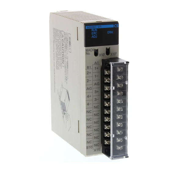
Components and Switch Settings Section 2-3 Components and Switch Settings CS1W-AD041-V1 CS1W-AD081-V1 Front Front With Terminal Block With Terminal Block Removed With Terminal Block With Terminal Block Removed Unit number Unit number setting switch setting switch External External terminal block... -
Page 51: Indicators
Section 2-3 Components and Switch Settings The terminal block is attached by a connector. It can be removed by loosening the two black mounting screws located at the top and bottom of the terminal block. Check to be sure that the black terminal block mounting screw is securely tightened to a torque of 0.5 N·m. -
Page 52: Unit Number Switch
Always turn OFF the power before setting the unit number. Use a flat-blade screwdriver, being careful not to damage the slot in the screw. Be sure not to leave the switch midway between settings. Switch CS1W-AD041-V1/AD081-V1 CS1W-AD161 (See note 2.) setting Unit... -
Page 53: Operation Mode Switch
1. The operation mode can be set in the DM Area as an alternative to using the operation mode switch. 2. Set the operation mode in DM word m+18 for CS1W-AD041-V1 and CS1W-AD081-V1, and in DM word m+19 for CS1W-AD161. -
Page 54: Voltage/Current Switch (Cs1W-Ad041-V1/Ad081-V1)
IN8: Input 8 IN7: Input 7 Note 1. There are only four inputs for the CS1W-AD041-V1. 2. With CS1W-AD161, select voltage/current input by wiring the connector terminals. !Caution Be sure to turn OFF the power to the PLC before mounting or removing the... -
Page 55: Wiring
Section 2-4 Wiring Wiring 2-4-1 Terminal Arrangement The signal names corresponding to the connecting terminals are as shown in the following diagram. CS1W-AD041-V1 Input 1 (+) Input 2 (+) Input 1 (–) Input 2 (–) Input 3 (+) Input 4 (+) Input 3 (–) -
Page 56: Internal Circuitry
Unit. Connecting shielded input lines can improve noise resistance. !Caution Do not make any connections to the N.C. terminals. 2-4-2 Internal Circuitry The following diagrams show the internal circuitry of the analog input section. Input Circuitry CS1W-AD041-V1/AD081-V1 15 k 15 k Input circuit Input (+) conversion... - Page 57 Section 2-4 Wiring CS1W-AD161 15 kΩ 15 kΩ Input (+) Input circuit 250 Ω 1 MΩ Current mode conversion circuit 15 kΩ 15 kΩ Input (−) 1 MΩ AG (analog 0 V) AG (common to all inputs) Internal Configuration Indicators/Switch Externally connected Multi-...
-
Page 58: Voltage Input Disconnection
Section 2-4 Wiring 2-4-3 Voltage Input Disconnection Connected device #1 Connected device #2 24 VDC Note If the connected device #2 in the above example outputs 5 V and the power supply is shared by 2 channels as shown in the above diagram, approximately one third of the voltage, or 1.6 V, will be input at input 1. -
Page 59: Input Wiring Example
1. When using current inputs, pins IN1 to IN8 (pins IN1 to IN4 for the CS1W- AD041-V1) of the voltage/current switch must be set to ON. Refer to 2-3-4 Voltage/Current Switch (CS1W-AD041-V1/AD081-V1) for further details. 2. For inputs that are not used, either set to “0: Not used” in the input number settings (refer to 2-6-1 Input Settings and Conversion Values) or short-cir- cuit the voltage input terminals (V+) and (V–). - Page 60 Section 2-4 Wiring CS1W-AD161 Use OMRON's XW2D-34G6 Connector-Terminal Conversion Unit and Special Connection Cable for input wiring. CS1W-AD161 Analog Input Unit CN2 (inputs 9 to 16) CN1 (inputs 1 to 8) XW2Z-200C XW2Z-200C Terminal Block Terminal Block Conversion Unit Conversion Unit...
-
Page 61: Input Wiring Considerations
Section 2-4 Wiring CN2 to Terminal Block Conversion A9 A10 A11 A12 A13 A14 A15 A16 A17 B9 B10 B11 B12 B13 B14 B15 B16 B17 Voltage Input Wiring Input n+ Voltage input n Current mode n − Input n− Shield Current Input Wiring Short-circuit the input(+) and current mode terminals when using current... -
Page 62: Exchanging Data With The Cpu Unit
2-5-1 Outline of Data Exchange Data is exchanged between the CPU Unit and the CS1W-AD041-V1/081-V1/ AD161 Analog Input Unit via the Special I/O Unit Area (for data used to oper- ate the Unit) and the Special I/O Unit DM Area (for data used for initial set- tings). -
Page 63: Unit Number Settings
The Special I/O Unit Area and Special I/O Unit DM Area word addresses that each Analog Input Unit occupies are set by the unit number switch on the front panel of the Unit. Switch CS1W-AD041-V1/AD081-V1 CS1W-AD161 (See note 2.) setting Unit... -
Page 64: Special I/O Unit Restart Bits
Special I/O Unit DM Area. Settings, such as the inputs used and the analog input signal range must be set in this area. CS1W-AD041-V1/AD081-V1 SYSMAC CS-series CPU Unit CS1W-AD041-V1/081-V1 Analog Input Unit (Special I/O Unit DM Area) (Fixed Data Area) Word... - Page 65 Exchanging Data with the CPU Unit Section 2-5 CS1W-AD161 CS1W-AD161 Analog Input Unit CS-series CPU Unit Special I/O Unit DM Area Allocated DM Area words Initial data Unit #0 D20000 to D20199 Input conversion D (m) enabled/disabled Unit #1 D20100 to D20299 Unit #2 D20200 to D20399 D (m+1)
- Page 66 Section 2-5 Exchanging Data with the CPU Unit DM Allocation Contents The following table shows the allocation of DM words and bits for both normal and adjustment mode. CS1W-AD041-V1 DM word Bits (See note.) D(m) Not used. (Settings are ignored.) Not used.
- Page 67 Exchanging Data with the CPU Unit Section 2-5 CS1W-AD161 DM word Bits (See note D(m) Input use setting Input Input Input Input Input Input Input Input Input Input Input Input Input Input Input Input D(m+1) Input range setting (inputs 1 to 8) Input 8 Input 7 Input 6...
- Page 68 Scaling setting Only set for CS1W-AD161 Note 1. For CS1W-AD041-V1 and CS1W-AD081-V1, the input signal range of “1 to 5 V” and “4 to 20 mA” is switched using the pins of the voltage/current switch. Refer to 2-3-4 Voltage/Current Switch (CS1W-AD041-V1/AD081- V1) for details.
-
Page 69: I/O Refresh Data Allocations
I/O refresh data for the Analog Input Unit is exchanged according to the allo- cations in the Special I/O Unit Area. CS1W-AD041-V1/AD081-V1 SYSMAC CS-series CPU Unit CS1W-AD041-V1/081-V1 Analog Input Unit (I/O Refresh Data Area) (Special I/O Unit Area) Normal mode... - Page 70 Exchanging Data with the CPU Unit Section 2-5 CS1W-AD161 CS1W-AD161 CS-series CPU Unit Analog Input Unit Special I/O Unit CIO Area Operation data Allocated addresses Normal mode Unit #0 CIO 2000 to CIO 2019 Unit #1 OUT refresh CIO 2010 to CIO 2029 CIO n I/O refresh Unit #2...
- Page 71 Section 2-5 Exchanging Data with the CPU Unit CS1W-AD041-V1 Word Bits Output Not used. Peak value hold (CPU to Input Input Input Input Unit) Input n + 1 Input 1 conversion value (Unit to CPU) n + 2 Input 2 conversion value...
- Page 72 Section 2-5 Exchanging Data with the CPU Unit CS1W-AD161 Word Bits Output Peak value hold (CPU to Input Input Input Input Input Input Input Input Input Input Input Input Input Input Input Input Unit) Input n + 1 Input 1 A/D conversion value (Unit to CPU) n + 2...
- Page 73 Input Input Input Input Input Note 1. Use settings 1 to 4 for the CS1W-AD041-V1. 2. With the CS1W-AD041-V1, bits 04 to 07 in word n+9 (disconnection detec- tion) are not used. CS1W-AD161 Word Bits Output Not used. Inputs to be adjusted (See note 2.)
- Page 74 Contents Input to be adjusted Sets input to be adjusted. Leftmost digit: 2 (fixed) Rightmost digit: 1 to 8 (1 to 4 for CS1W-AD041-V1) Offset (Offset Bit) When ON, adjusts offset error. Gain (Gain Bit) When ON, adjusts gain error.
-
Page 75: Analog Input Functions And Operating Procedures
00: −10 to 10 V 01: 0 to 10 V 10: 1 to 5 V / 4 to 20 mA 11: 0 to 5 V Note There are only four inputs for the CS1W-AD041-V1. CS1W-AD161 Input 8 Input 6 Input 6... - Page 76 Reading Conversion Analog input conversion values are read in 4-digit hexadecimal for each input. Values Address CS1W-AD161 CS1W-AD081-V1 CS1W-AD041-V1 Input 1 conversion value Input 1 conversion value Input 1 conversion value Input 2 conversion value Input 2 conversion value Input 2 conversion value...
-
Page 77: Conversion Time/Resolution Setting
Conversion Time/Resolution Setting The default setting is a conversion cycle of 1 ms and resolution of 4,000. For even higher speed and precision, change the settings in bits 08 to 15. CS1W-AD041-V1/AD081-V1 D (m+18) Conversion time/resolution setting Operation mode setting... -
Page 78: Mean Value Processing
Specify whether or not to use mean value processing and the number of his- tory buffers to be used for mean value processing. Address CS1W-AD161 CS1W-AD081-V1 CS1W-AD041-V1 Set value D(m+2) Input 1 Input 1 0000: Mean value processing with 2 buffers... - Page 79 Section 2-6 Analog Input Functions and Operating Procedures Unit Restart Bit to transfer the contents of the DM settings to the Special I/O Unit. The history buffer operational means are calculated as shown below. (In this example, there are four buffers.) 1,2,3...
- Page 80 Section 2-6 Analog Input Functions and Operating Procedures When a disconnection is restored, the mean value processing function begins again from step 1. Note 1. The default setting for mean value processing in the Analog Input Unit is mean value processing with 2 buffers. The response time for the default setting is different from when there is no mean processing, as shown in the following diagram.
-
Page 81: Peak Value Hold Function
The peak value hold function can be set individually for each input number by turning on the respective bits (00 to 07 for CS1W-AD081-V1, 00 to 03 for CS1W-AD041-V1) in CIO word n. Word n n = D20000 + unit number x 10... -
Page 82: Input Disconnection Detection Function
Setting 0: Not used (the conversion value is reset when the bit turns OFF) 1: Peak value hold function is used (held while ON) • CS1W-AD041-V1: Inputs 1 to 4 • CS1W-AD081-V1: Inputs 1 to 8 For the CIO word addresses, n = CIO 2000 + (unit number x 10). -
Page 83: Scaling Function (Cs1W-Ad161 Only)
Section 2-7 Adjusting Offset and Gain In the following example, the conversion value is read only if there is no dis- connection at analog input number 1. (The unit number is 0.) 200901 The conver- MOV (021) sion value in 2001 CIO word 2001 (input... - Page 84 Section 2-7 Adjusting Offset and Gain The following diagram shows the flow of operations when using the adjust- ment mode for adjusting offset and gain. Set the operation mode to adjustment mode. Set the operation mode switch, or (for version-1 Unit) set the operation mode in DM Area word m+18 (see note), to adjustment mode.
-
Page 85: Input Offset And Gain Adjustment Procedures
Word n adjusted 1 to 8 (See note.) n = CIO 2000 + unit number x 10 2: Input (fixed) Note Use inputs 1 to 4 for the CS1W-AD041-V1. CS1W-AD161 Input numbers to be adjusted 1 to 16 Not used. - Page 86 ^ OFF 200100 ^ ON For CS1W-AD041-V1 and CS1W-AD081-V1, the analog input’s digital conversion values while the Offset Bit is ON will be monitored in CIO word n+8. For CS1W-AD161, the values will be monitored in CIO word n+17. 2. Check whether the input devices are connected.
- Page 87 Section 2-7 Adjusting Offset and Gain Wiring for Voltage Input CS1W-AD041-V1/081-V1 Voltage input – Input 1 CS1W-AD161 Input n+ Current mode n Voltage n − Input n− Shield Wiring for Current Input When using current input, short-circuit the input (+) terminal and the current mode terminal.
- Page 88 Section 2-7 Adjusting Offset and Gain 4. After inputting the voltage or current so that the conversion value for the analog input terminal is 0000, turn ON bit 04 (the Set Bit) of CIO word n+1, and then turn it OFF again. CONT SHIFT 200104...
- Page 89 ^ OFF 200101 ^ ON For CS1W-AD041-V1 and CS1W-AD081-V1, the analog input’s digital conversion values while the Gain Bit is ON will be monitored in CIO word n+8. For CS1W-AD161, the values will be monitored in CIO word n+17. 2. Check whether the input devices are connected.
- Page 90 Section 2-7 Adjusting Offset and Gain Wiring for Current Input When using current input, short-circuit the input (+) terminal and the current mode terminal. CS1W-AD041-V1/081-V1 Current input – Input 1 For current input, check that the voltage/ current switch is ON.
- Page 91 Section 2-7 Adjusting Offset and Gain 5. To finish the gain adjustment, turn OFF bit 01 (the Gain Bit) of CIO word n+1. CONT SHIFT 200101 ^ ON 200101 ^ OFF RESET !Caution Do not turn OFF the power supply or restart the Unit while the Set Bit is ON (data is being written to the EEPROM).
-
Page 92: Handling Errors And Alarms
Section 2-8 Handling Errors and Alarms While the Clear Bit is ON, the adjusted value will be cleared and reset to the default offset and gain values when the Set Bit turns ON. 3. To finish the clearing of adjusted values, turn OFF bit 05 (the Clear Bit) of CIO word n+1. -
Page 93: Alarms Occurring At The Analog Input Unit
4 to 20 mA. CS1W-AD041-V1/AD081-V1 Disconnection Detection Flags (See note.) Word n+9 Alarm Flags m = D20000 + unit number x 10 Note Use inputs 1 to 4 for the CS1W-AD041-V1. CS1W-AD161 Disconnection Detection Flags Word n+18 Word n+19 Alarm Flags Not used. - Page 94 1. These alarms are output in word n+9 for CS1W-AD041-V1 and CS1W- AD081-V1, and in words n+18/n+19 for CS1W-AD161. 2. The CS1W-AD041-V1 uses bits 00 to 08 of word n+9, and the CS1W- AD081-V1 uses bits 00 to 04. The CS1W-AD161 uses bits 00 to 15 of word n+18.
- Page 95 3. These alarms are output in CIO word n+8 for CS1W-AD041-V1 and CS1W-AD081-V1, and in CIO word n+18 for CS1W-AD161. 4. The operation mode is set in DM word m+18 for CS1W-AD041-V1 and CS1W-AD081-V1, and in DM word m+19 for CS1W-AD161.
-
Page 96: Errors In The Cpu Unit
Mode Setting and data Error becomes 0000. Note These alarms are output in CIO word n+9 for CS1W-AD041-V1 and CS1W- AD081-V1, and in CIO word n+19 for CS1W-AD161. 2-8-3 Errors in the CPU Unit When errors occur in the CPU Unit or I/O bus, and I/O refresh with the Special I/O Unit is not performed correctly resulting in the Analog Input Unit malfunc- tioning, the ERH indicator will be lit. -
Page 97: Restarting Special I/O Units
Handling Errors and Alarms Section 2-8 The unit number for the Analog Input Unit has not been set correctly. Error Error contents Input status Duplicate Unit Number The same unit number has been Conversion does not start and (See note.) assigned to more than one Unit data becomes 0000. - Page 98 Section 2-8 Handling Errors and Alarms Value Does Not Change as Intended Probable cause Countermeasure Page The input device’s signal range Check the specifications of the does not match the input signal input device, and match the settings range for the relevant input number for the input signal ranges.
- Page 99 Section 2-8 Handling Errors and Alarms...
- Page 100 SECTION 3 CJ-series Analog Input Units This section explains how to use the CJ1W-AD041-V1/081-V1 Analog Input Unit. Specifications ..........3-1-1 Specifications .
-
Page 101: Specifications
Section 3-1 Specifications Specifications 3-1-1 Specifications Item CJ1W-AD041-V1 CJ1W-AD081-V1 Unit type CJ-series Special I/O Unit Isolation (See note 1.) Between I/O and PLC signals: Photocoupler (No isolation between individual I/O signals.) External terminals 18-point detachable terminal block (M3 screws) Affect on CPU Unit cycle time 0.2 ms Power consumption 420 mA max. - Page 102 3. The maximum number of Analog Input Units that can be mounted to one Rack varies depending on the current consumption of the other Units mounted to the Rack. Power Supply Unit Rack CJ1W-DA021 CS1W-AD041-V1 CJ1W-MAD42 CJ1W-DA041 CJ1W-AD081-V1 (5 VDC 580 mA) (5 VDC 120 mA)
-
Page 103: Input Function Block Diagram
Section 3-1 Specifications 3-1-2 Input Function Block Diagram Analog Input Unit CPU Unit Special I/O Unit Area Mean value Peak value refresh processing hold function Analog Input dis- disabled disabled input 1 Analog input 1 connection conver- detection sion Mean value Peak value value hold function... - Page 104 Section 3-1 Specifications Range: 0 to 10 V Conversion value 1068 (20D0) 0FA0 (1F40) Resolution: 4,000 (Resolution: 8,000) 0000 (0000) FF38 (FE70) 10 V –0.5 V 10.5 V Analog input signal Range: 0 to 5 V Conversion value 1068 (20D0) 0FA0 (1F40) Resolution: 4,000 (Resolution: 8,000)
- Page 105 Section 3-1 Specifications Range: –10 to 10 V Conversion value 0898 (1130) 07D0 (0FA0) Resolution: 4,000 (Resolution: 8,000) 0000 (0000) F830 (F060) F768 (EED0) –10 V 10 V –11 V 11 V Analog input signal Note The conversion values for a range of –10 to 10 V will be as follows (for a reso- lution of 4,000): 16-bit binary data F768...
-
Page 106: Operating Procedure
Section 3-2 Operating Procedure Operating Procedure Follow the procedure outlined below when using Analog Input Units. Installation and Settings 1,2,3... 1. Set the operation mode to normal mode. Set the DIP switch on the front panel of the Unit, or set the operation mode in DM word m+18, to normal mode. -
Page 107: Procedure Examples
Section 3-2 Operating Procedure 3-2-1 Procedure Examples CJ1W-AD041-V1 CJ-series CPU Unit CJ1W-AD081-V1 AD081 IN1: 1 to 5 V IN2: 1 to 5 V MACH IN3: 4 to 20 mA Analog inputs IN4: 4 to 20 mA IN5: 0 to 10 V IN6: 0 to 10 V IN7: -10 to 10V MODE... - Page 108 Section 3-2 Operating Procedure 3. Set the unit number switch. Refer to 3-3-2 Unit Number Switch for further details. AD081 If the unit number is set to 1, words will MACH be allocated to the Analog Input Unit in Special I/O Unit Area CIO 2010 to MACH CIO 2019 and in the Special I/O Unit Area D20100 to D20199.
- Page 109 Section 3-2 Operating Procedure Initial Data Settings 1,2,3... 1. Specify the Special I/O Unit DM Area settings. Refer to 3-5-4 Fixed Data Allocations for further details. Peripheral port AD081 DA041 OD261 Analog input 1: 1 to 5 V SYSMAC ERR/ALM CJ1G-CPU44 9 10 11 12 13 14 15 PROGRAMMABLE...
- Page 110 Section 3-2 Operating Procedure • The following diagram shows the conversion time/resolution setting. (Refer to 3-6-2 Conversion Time/Resolution Setting .) 14 13 12 11 10 09 08 07 06 05 04 03 01 00 m+18: D20118 (0000 Hex) Conversion Time/Resolution Setting 0000: 1-ms conversion time, 4,000 resolution C100: 250- µ...
- Page 111 Section 3-2 Operating Procedure 2. Set as required. 201900 Input 1 Disconnection Detection Flag (See note 3.) For 1 to 5 V, the hexadecimal value 0000 MOV (021) to 0FA0 will be stored in CIO 2011, so if there is no disconnection (i.e., 201900 is 2011 OFF), CIO 2011 will be stored in D00100...
-
Page 112: Components And Switch Settings
Section 3-3 Components and Switch Settings Components and Switch Settings CJ1W-AD041-V1 CJ1W-AD081-V1 Front With Terminal Block With Terminal Block Removed Indicators AD081 AD081 Terminal block MACH MACH Unit number Voltage/current setting switch switch MODE MODE Terminal block DIN Track mounting pin Terminal block lock lever Operating mode switch (pull down to release... -
Page 113: Indicators
Section 3-3 Components and Switch Settings The terminal block is attached using a connector mechanism. It can be removed by lowering the lever at the bottom of the terminal block. The lever must normally be in the raised position. Confirm this before opera- tion. -
Page 114: Operation Mode Switch
Section 3-3 Components and Switch Settings Always turn OFF the power before setting the unit number. Use a flat-blade screwdriver, being careful not to damage the slot in the screw. Be sure not to leave the switch midway between settings. Switch Unit Special/O Unit Area... -
Page 115: Voltage/Current Switch
Section 3-3 Components and Switch Settings Relationship between Operation Mode Setting and Hardware Operation Mode Switch Hardware operation Setting of bits 00 to 07 of Operation mode when mode switch m+18 power is turned ON or Unit is restarted Normal mode Normal mode Normal mode Normal mode... -
Page 116: Wiring
Section 3-4 Wiring Wiring 3-4-1 Terminal Arrangement The signal names corresponding to the connecting terminals are as shown in the following diagram. CJ1W-AD041-V1 Input 2 (+) Input 1 (+) Input 2 (–) Input 1 (–) Input 4 (+) Input 3 (+) Input 4 (–) Input 3 (–) N.C. -
Page 117: Internal Circuitry
Section 3-4 Wiring 3-4-2 Internal Circuitry The following diagrams show the internal circuitry of the analog input section. Input Circuitry 15 k 15 k Input (+) Input circuit conversion 15 k 15 k circuit Input (–) Voltage/ current input switch (analog 0 V) AG (common to all inputs) -
Page 118: Voltage Input Disconnection
Section 3-4 Wiring 3-4-3 Voltage Input Disconnection Connected device #1 Connected device #2 24 VDC Note If the connected device #2 in the above example outputs 5 V and the power supply is shared by 2 channels as shown in the above diagram, approximately one third of the voltage, or 1.6 V, will be input at input 1. -
Page 119: Input Wiring Example
Section 3-4 Wiring 3-4-4 Input Wiring Example CJ1W-AD081-V1 Input 2 − Input 1 − Input 4 − Input 3 − Input 6 − Input 5 − Input 8 − Input 7 − Note There are only four inputs for the CJ1W-AD041-V1. Inputs 5 to 8 are not used. -
Page 120: Exchanging Data With The Cpu Unit
Section 3-5 Exchanging Data with the CPU Unit • If there is noise interference from power lines (if, for example, the power supply is shared with electrical welding devices or electrical discharge machines, or if there is a high-frequency generation source nearby) install a noise filter at the power supply input area. -
Page 121: Unit Number Settings
Section 3-5 Exchanging Data with the CPU Unit 3-5-2 Unit Number Settings The Special I/O Unit Area and Special I/O Unit DM Area word addresses that each Analog Input Unit occupies are set by the unit number switch on the front panel of the Unit. -
Page 122: Fixed Data Allocations
Section 3-5 Exchanging Data with the CPU Unit 3-5-4 Fixed Data Allocations DM Allocation and The initial settings of the Analog Input Unit are set according to the data allo- Contents cated in the Special I/O Unit DM Area. Settings, such as the inputs used and the analog input signal range must be set in this area. - Page 123 Section 3-5 Exchanging Data with the CPU Unit DM Allocation Contents The following table shows the allocation of DM words and bits for both normal and adjustment mode. CJ1W-AD041-V1 DM word Bits D(m) Not used. (Settings are ignored.) Not used. Input use setting Input Input...
-
Page 124: I/O Refresh Data Allocations
Section 3-5 Exchanging Data with the CPU Unit Set Values and Stored Values Item Contents Page Input Use setting Not used. Used. Input signal range 00: –10 to 10 V 01: 0 to 10 V 10: 1 to 5 V/4 to 20 mA (See note 1.) 11: 0 to 5 V Mean value processing set- 0000:... - Page 125 Section 3-5 Exchanging Data with the CPU Unit 2. If two or more Special I/O Units are assigned the same unit number, a “UNIT No. DPL ERR” error (in the Programming Console) will be generat- ed (A40113 will turn ON) and the PLC will not operate. Allocations for Normal For normal mode, set the operation mode switch on the front panel of the Unit Mode...
- Page 126 Section 3-5 Exchanging Data with the CPU Unit Set Values and Stored Values Item Contents Page Input Peak value hold function Not used. Peak value hold used. Conversion value 16-bit binary data Calculation result Disconnection detection No disconnection Disconnection Common Alarm Flags Bits 00 to 03: Disconnection detection 102,121...
-
Page 127: Analog Input Functions And Operating Procedures
Section 3-6 Analog Input Functions and Operating Procedures Set Values and Stored Refer to 3-7-1 Adjustment Mode Operational Flow for further details. Values Item Contents Input to be adjusted Sets input to be adjusted. Leftmost digit: 2 (fixed) Rightmost digit: 1 to 8 (1 to 4 for CJ1W-AD041-V1) Offset (Offset Bit) When ON, adjusts offset error. - Page 128 Section 3-6 Analog Input Functions and Operating Procedures Note Use 250 µ s instead of 1 ms is set to a conversion time of 250 µ s and resolution of 8,000. The conversion values in words for inputs that have been set to “Not used” will always be “0000.”...
-
Page 129: Conversion Time/Resolution Setting
Section 3-6 Analog Input Functions and Operating Procedures Example 1 In this example, the conversion data from only one input is read. (The unit number is 0.) Input condition Conversion data in CIO word MOV(021) 2001 (input number 1) is read 2001 to D 00001. -
Page 130: Mean Value Processing
Section 3-6 Analog Input Functions and Operating Procedures 3-6-3 Mean Value Processing The Analog Input Unit can compute the mean value of the conversion values of analog inputs that have been previously sampled. Mean value processing involves an operational mean value in the history buffers, so it has no effect on the data refresh cycle. - Page 131 Section 3-6 Analog Input Functions and Operating Procedures 1,2,3... 1. With the first cycle, Data 1 is stored in all the history buffers. Data 1 Data 1 (Mean value Conversion value processing) Data 1 Data 1 Mean value = (Data 1 + Data 1 + Data 1 + Data 1) ÷ 4 2.
- Page 132 Section 3-6 Analog Input Functions and Operating Procedures setting is different from when there is no mean processing, as shown in the following diagram. 2. Specify “no mean value processing” to follow conversion of a rapid change in input signals. 3.
-
Page 133: Peak Value Hold Function
Section 3-6 Analog Input Functions and Operating Procedures Calculation Example The following example calculations are for a resolution of 8,000 with an appli- cation using inputs 1 and 8, 64 averaging buffers set for input 1, and no aver- aging set for input 8. •... -
Page 134: Input Disconnection Detection Function
Analog Input Functions and Operating Procedures Section 3-6 3-6-5 Input Disconnection Detection Function When an input signal range of 1 to 5 V (4 to 20 mA) is used, input circuit dis- connections can be detected. The detection conditions for each of the input signal ranges are shown in the following table. -
Page 135: Adjusting Offset And Gain
Adjusting Offset and Gain Section 3-7 Adjusting Offset and Gain 3-7-1 Adjustment Mode Operational Flow The adjustment mode enables the input of the connected devices to be cali- brated. The offset voltage (or current) and gain voltage (or current) at the output device are entered as analog input conversion data 0000 and 0FA0 (07D0 if the range is ±... - Page 136 Section 3-7 Adjusting Offset and Gain The following diagram shows the flow of operations when using the adjust- ment mode for adjusting offset and gain. Set the operation mode to adjustment mode. Set the operation mode switch, or set the operation mode in DM Area word m+18, to adjustment mode.
-
Page 137: Input Offset And Gain Adjustment Procedures
Input to be adjusted (1 to 8) 2: Input (fixed) (1 to 4 for CS1W-AD041-V1) For the CIO word addresses, n = CIO 2000 + (unit number x 10). The following example uses input number 1 adjustment for illustration. (The unit number is 0.) - Page 138 Section 3-7 Adjusting Offset and Gain Offset Adjustment The procedure for adjusting the analog input offset is explained below. As shown in the following diagram, the offset is adjusted by sampling inputs so that the conversion value becomes 0. 0FA0 Input signal range: 0 to 10 V 10 V...
- Page 139 Section 3-7 Adjusting Offset and Gain 3. Input the voltage or current so that the conversion value becomes 0000. The following table shows the offset adjustment voltages and currents to be input according to the input signal range. Input signal range Input range Word (n+8) monitoring value...
- Page 140 Adjusting Offset and Gain Section 3-7 Gain Adjustment The procedure for adjusting the analog input gain is explained below. As shown in the following diagram, the gain is adjusted by sampling inputs so that the conversion value is maximized. Gain adjustment input range 0FA0 Input signal range: 0 to 10 V...
- Page 141 Section 3-7 Adjusting Offset and Gain 3. Input the voltage or current so that the conversion value is maximized (0FA0 or 07D0 at a resolution of 4,000). The following table shows the gain adjustment voltages and currents to be input according to the input signal range.
- Page 142 Section 3-7 Adjusting Offset and Gain Clearing Offset and Gain Follow the procedure outlined below to return the offset and gain adjusted val- Adjusted Values ues to their default settings. The following example uses input number 1 adjustment for illustration. (The unit number is 0.) 1,2,3...
-
Page 143: Handling Errors And Alarms
Section 3-8 Handling Errors and Alarms Handling Errors and Alarms 3-8-1 Indicators and Error Flowchart Indicators If an alarm or error occurs in the Analog Input Unit, the ERC or ERH indica- tors on the front panel of the Unit will light. Front panel of Unit Meaning Indicator... -
Page 144: Alarms Occurring At The Analog Input Unit
Handling Errors and Alarms Section 3-8 3-8-2 Alarms Occurring at the Analog Input Unit When an alarm occurs at the Analog Input Unit, the ERC indicator lights and the Alarm Flags are stored in bits 08 to 15 of CIO word n+9. 15 14 09 08 04 03... - Page 145 Handling Errors and Alarms Section 3-8 ERC Indicator and RUN Indicator: Lit, ADJ Indicator: Flashing : Lit : Flashing : Not lit This alarm will occur in the case of incorrect operation while in the adjustment mode. In adjustment mode, the Adjustment Mode ON Flag will turn ON in bit 15 of CIO word n+9.
-
Page 146: Errors In The Cpu Unit
Section 3-8 Handling Errors and Alarms 3-8-3 Errors in the CPU Unit When errors occur in the CPU Unit or I/O bus, and I/O refresh with the Special I/O Unit is not performed correctly resulting in the Analog Input Unit malfunc- tioning, the ERH indicator will be lit. -
Page 147: Restarting Special I/O Units
Handling Errors and Alarms Section 3-8 3-8-4 Restarting Special I/O Units There are two ways to restart Special I/O Unit operation after having changed DM contents or having cleared the cause of an error. The first way is to turn the power to the PLC OFF and ON, and the second way is to turn ON the Special I/O Unit Restart Bit ON. -
Page 148: Cs-Series Analog Output Units
SECTION 4 CS-series Analog Output Units This section explains how to use the CS1W-DA041/08V/08C Analog Output Units. Specifications ..........4-1-1 Specifications . -
Page 149: Specifications
Section 4-1 Specifications Specifications 4-1-1 Specifications Item CS1W-DA041 CS1W-DA08V CS1W-DA08C Unit type CS-series Special I/O Unit Isolation (See note 1.) Between I/O and PLC signals: Photocoupler (No isolation between individual I/O signals.) External terminals 21-point detachable terminal block (M3 screws) Power consumption 130 mA max. - Page 150 Specifications Section 4-1 2. Refer to Dimensions on page 359 for details on the Unit’s dimensions. 3. Maximum Number of Units Power Supply CS1W-DA041/08V CS1W-DA08C Unit C200HW-PA204 3 Units max. 2 Units max. C200HW-PA204S C200HW-PA204R C200HW-PD204 C200HW-PA209R 7 Units max. 5 Units max.
-
Page 151: Output Function Block Diagram
Section 4-1 Specifications 4-1-2 Output Function Block Diagram Analog Output Unit CPU Unit Special I/O Unit Area Output hold enabled Analog Analog output 1 output 1 set value Output hold disabled Analog output 2 Same as above. Analog output 3 Same as above. - Page 152 Section 4-1 Specifications Range: 0 to 10 V Analog output signal 10.5 V 10 V –0.5 V 0000 0FA0 FF38 Resolution: 4,000 1068 Set value (16-bit binary data) Range: 0 to 5 V Analog output signal 5.25 V –0.25 V 0000 0FA0 FF38...
-
Page 153: Operating Procedure
Section 4-2 Operating Procedure Range: − 10 to 10 V Analog output signal 11 V 10 V –10 V –11 V 0000 F830 07D0 Resolution: 4,000 0898 F768 Set value (16-bit binary data) Note The set values for a range of –10 to 10 V will be as follows: 16-bit binary data F768 –2200... -
Page 154: Procedure Examples
Section 4-2 Operating Procedure Offset and Gain Adjustment 1,2,3... 1. Set the operation mode switch on the rear panel of the Unit to adjustment mode. 2. Turn ON the power to the PLC. 3. Adjust the offset and gain. 4. Turn OFF the power to the PLC. 5. - Page 155 Section 4-2 Operating Procedure 2. Mount and wire the Analog Output Unit. Refer to 1-2-1 Mounting Proce- dure, 4-4 Wiring or 4-4-3 Output Wiring Example for further details. 3. Set the unit number switch. Refer to 4-3-2 Unit Number Switch for further details.
- Page 156 Section 4-2 Operating Procedure Creating I/O Tables After turning ON the power to the PLC, be sure to create the I/O tables. Peripheral port Initial Data Settings 1,2,3... 1. Specify the Special I/O Unit DM Area settings. Refer to DM Allocation Con- tents on page 145 for further details.
- Page 157 Section 4-2 Operating Procedure • The following diagram shows the output range settings. Refer to 4-6-1 Output Settings and Conversions for more details. Output 1: 1 to 5 V. Set to 10. Output 2: 1 to 5 V. Set to 10. Output 3: –10 to 10 V.
- Page 158 Section 4-2 Operating Procedure The following table shows the addresses used for analog output. Output number Output signal Output setting Original range address conversion address (n = CIO 2010) See note 1. 1 to 5 V (n+1) = CIO 2011 D00200 0 to 10 V (n+2) = CIO 2012...
-
Page 159: Components And Switch Settings
Section 4-3 Components and Switch Settings Components and Switch Settings Front CS1W-DA041 CS1W-DA08V CS1W-DA08C Unit number setting switch External ter- minal block mounting screws (black M3) External terminal block (M3) Back Side Terminal block Operation mode switch Backplane connector... -
Page 160: Indicators
Section 4-3 Components and Switch Settings The terminal block is attached by a connector. It can be removed by loosening the two black mounting screws located at the top and bottom of the terminal block. Check to be sure that the black terminal block mounting screw is securely tightened to a torque of 0.5 N·m. -
Page 161: Unit Number Switch
Section 4-3 Components and Switch Settings 4-3-2 Unit Number Switch The CPU Unit and Analog Output Unit exchange data via the Special I/O Unit Area and the Special I/O Unit DM Area. The Special I/O Unit Area and Special I/O Unit DM Area word addresses that each Analog Output Unit occupies are set by the unit number switch on the front panel of the Unit. -
Page 162: Wiring
Section 4-4 Wiring Wiring 4-4-1 Terminal Arrangement The signal names corresponding to the connecting terminals are as shown in the following diagram. CS1W-DA08V/08C N.C. N.C. Output 1 (+) Output 2 (+) Output 1 (–) Output 2 (–) Output 3 (+) Output 4 (+) Output 3 (–) Output 4 (–) -
Page 163: Internal Circuitry
Section 4-4 Wiring 4-4-2 Internal Circuitry The following diagrams show the internal circuitry of the analog output sec- tion. Voltage Output Circuitry Voltage output section for CS1W-DA08V/DA041 Output switch and Voltage conversion output (+) circuit Voltage output (–) AG (common to all outputs) Current Output Circuitry Current output section for CS1W-DA08C/DA041 Output... -
Page 164: Output Wiring Example
Wiring Section 4-4 4-4-3 Output Wiring Example CS1W-DA08V/08C Output 1 Output 2 Shield Output 3 Output 4 Output 5 Output 6 Shield Output 7 Output 8 CS1W-DA041 Output 2 Output 1 (Voltage output) (Voltage output) Output 3 Output 4 (Current output) (Current output) Note Crimp-type terminals must be used for terminal connections, and the screws must be tightened securely. -
Page 165: Exchanging Data With The Cpu Unit
Exchanging Data with the CPU Unit Section 4-5 4-4-4 Output Wiring Considerations When wiring outputs, apply the following points to avoid noise interference and optimize Analog Output Unit performance. • Use two-core shielded twisted-pair cables for output connections. • Route output cables separately from the AC cable, and do not run the Unit’s cables near a main circuit cable or a high voltage cable. -
Page 166: Unit Number Settings
Section 4-5 Exchanging Data with the CPU Unit 4-5-2 Unit Number Settings The Special I/O Unit Area and Special I/O Unit DM Area word addresses that each Analog Output Unit occupies are set by the unit number switch on the front panel of the Unit. -
Page 167: Fixed Data Allocations
Exchanging Data with the CPU Unit Section 4-5 4-5-4 Fixed Data Allocations DM Allocation and The initial settings of the Analog Output Unit are set according to the data Contents allocated in the Special I/O Unit DM Area. Settings, such as the outputs used, and the analog output signal ranges must be set in this area. - Page 168 Section 4-5 Exchanging Data with the CPU Unit DM Allocation Contents The following table shows the allocation of DM words and bits for both normal and adjustment mode. CS1W-DA08V/08C DM word Bits D(m) Not used. Output use setting Out- Out- Out- Out- Out-...
-
Page 169: I/O Refresh Data Allocations
Section 4-5 Exchanging Data with the CPU Unit 4-5-5 I/O Refresh Data Allocations I/O refresh data for the Analog Output Unit is exchanged according to the allo- cations in the Special I/O Unit Area. SYSMAC CS-series CPU Unit CS1W-DA08V/08C/041 Analog Output Unit (Special I/O Unit Area) (I/O Refresh Data Area) Normal mode... - Page 170 Exchanging Data with the CPU Unit Section 4-5 Allocations for Normal For normal mode, set the operation mode switch on the rear panel of the Unit Mode as shown in the following diagram. The allocation of words and bits in the CIO Area is shown in the following table.
- Page 171 Section 4-5 Exchanging Data with the CPU Unit Set Values and Stored Values Item Contents Page Output Conversion enable 0: Conversion output stopped. 1: Conversion output begun. Set value 16-bit binary data Output setting error 0: No error 1: Output setting error Common Alarm Flags Bits 00 to 03: Output set value error...
-
Page 172: Analog Output Functions And Operating Procedures
Section 4-6 Analog Output Functions and Operating Procedures Set Values and Stored Refer to 4-7 Adjusting Offset and Gain or 4-8-2 Alarms Occurring at the Ana- Values log Output Unit for further details. Item Contents Output to be adjusted Sets output to be adjusted. Leftmost digit: 1 (fixed) Rightmost digit: 1 to 8 (1 to 4 for CS1W-DA041) Offset (Offset Bit) - Page 173 Section 4-6 Analog Output Functions and Operating Procedures Output Signal Range Any of four types of output signal range (–10 to 10 V, 0 to 10 V, 1 to 5 V/4 to 20 mA, and 0 to 5 V) can be selected for each of the outputs. To specify the output signal range for each output, use a Programming Device to set the D(m+1) bits in the DM Area shown in the following diagram.
-
Page 174: Starting And Stopping Conversion
Section 4-6 Analog Output Functions and Operating Procedures Example 2 In this example, multiple set values are written. (The unit number is #0.) Input condition XFER(070) The set values stored in D 00001 #0004 to D 00004 are written to CIO words 2001 to 2004 (outputs 1 to 4). -
Page 175: Output Hold Function
Section 4-6 Analog Output Functions and Operating Procedures 4-6-3 Output Hold Function The Analog Output Unit stops conversion under the following circumstances and outputs the value set by the output hold function. 1,2,3... 1. When the Conversion Enable Bit is OFF. Refer to Allocations for Normal Mode on page 147 and 4-6-2 Starting and Stopping Conversion. -
Page 176: Output Setting Errors
Section 4-7 Adjusting Offset and Gain Note After specifying the DM settings from a Programming Device, it will be neces- sary to either turn the power to the PLC OFF and ON, or turn ON the Special I/O Unit Restart Bit to transfer the contents of the DM settings to the Special I/ O Unit. - Page 177 Section 4-7 Adjusting Offset and Gain The following diagram shows the flow of operations when using the adjust- ment mode for adjusting offset and gain. Set the operation mode switch to adjustment mode. Set the operation mode switch on the rear panel of the Unit to adjustment mode.
-
Page 178: Output Offset And Gain Adjustment Procedures
Section 4-7 Adjusting Offset and Gain !Caution Set the PLC to PROGRAM mode when using the Analog Output Unit in adjustment mode. If the PLC is in MONITOR mode or RUN mode, the Analog Output Unit will stop operating, and the output values that existed immediately before this stoppage will be retained. - Page 179 Section 4-7 Adjusting Offset and Gain Offset Adjustment The procedure for adjusting the analog output offset is explained below. As shown in the following diagram, the set value is adjusted so that the analog output reaches the standard value (0 V/1 V/4 mA). 10 V Output signal range: 0 to 10 V...
- Page 180 Section 4-7 Adjusting Offset and Gain 4. Change the set value so that the output voltage are as shown in the follow- ing table. The data can be set within the indicated ranges. Output signal range Possible output Output range voltage/current adjustment 0 to 10 V...
- Page 181 Section 4-7 Adjusting Offset and Gain The bit will remain ON until the output becomes an appropriate value, at which time, it will turn OFF. 200102 ^ ON 200102 ^ OFF RESET 5. Check the 0-V/1-V/4-mA output, and then turn bit 04 (the Set Bit) of CIO word n+1 ON and then OFF again.
- Page 182 Section 4-7 Adjusting Offset and Gain Gain Adjustment The procedure for adjusting the analog output gain is explained below. As shown in the following diagram, the set value is adjusted so that the analog output is maximized (to 10 V/5 V/20 mA). Gain adjustment output range 10 V Output signal range:...
- Page 183 Section 4-7 Adjusting Offset and Gain 4. Change the set value so that the output voltage is as shown in the following table. The data can be set within the indicated ranges. Output signal range Possible output Output range voltage/current adjustment 0 to 10 V 9.5 to 10.5 V...
- Page 184 Section 4-7 Adjusting Offset and Gain The bit will remain ON until the output voltage becomes an appropriate val- ue, at which time, the output will turn OFF. 200102 ^ ON 200102 ^ OFF RESET 5. Check the 10V/5V/20 mA output, and then turn bit 04 (the Set Bit) of CIO word n+1 ON and then OFF again.
- Page 185 Section 4-7 Adjusting Offset and Gain Clearing Offset and Gain Follow the procedure outlined below to return the offset and gain adjusted val- Adjusted Values ues to their default settings. The following example uses output number 1 adjustment for illustration. (The unit number is 0.) 1,2,3...
-
Page 186: Handling Errors And Alarms
Section 4-8 Handling Errors and Alarms Handling Errors and Alarms 4-8-1 Indicators and Error Flowchart Indicators If an alarm or error occurs in the Analog Output Unit, the ERC or ERH indica- tors on the front panel of the Unit will light. Front panel of Unit Meaning Indicator... -
Page 187: Alarms Occurring At The Analog Output Unit
Section 4-8 Handling Errors and Alarms 4-8-2 Alarms Occurring at the Analog Output Unit When an alarm occurs at the Analog Output Unit, the ERC indicator lights and the Alarm Flags are stored in bits 08 to 15 of CIO word n+9. 15 14 09 08 01 00... -
Page 188: Errors In The Cpu Unit
Section 4-8 Handling Errors and Alarms ERC Indicator and RUN Indicator: Lit, ADJ Indicator: Flashing : Lit : Flashing : Not lit This alarm will occur in the case of incorrect operation while in the adjustment mode. In adjustment mode, the Adjustment Mode ON Flag will turn ON in bit 15 of CIO word n+9. -
Page 189: Restarting Special I/O Units
Section 4-8 Handling Errors and Alarms The ERH and RUN indicators will be lit if an error occurs in the I/O bus caus- ing a WDT (watchdog timer) error in the CPU Unit, resulting in incorrect I/O refresh with the Analog Output Unit. Turn ON the power supply again or restart the system. -
Page 190: Troubleshooting
Section 4-8 Handling Errors and Alarms 4-8-5 Troubleshooting The following tables explain the probable causes of troubles that may occur, and the countermeasures for dealing with them. Analog Output Does Not Change Probable Cause Countermeasure Page The output is not set for being used. Set the output for being used. The output hold function is in opera- Turn ON the Output Conversion tion. - Page 191 Section 4-8 Handling Errors and Alarms...
-
Page 192: Cj-Series Analog Output Unit
SECTION 5 CJ-series Analog Output Unit This section explains how to use the CJ1W-DA021/041/08V/08C Analog Output Units. Specifications ..........5-1-1 Specifications . -
Page 193: Specifications
Section 5-1 Specifications Specifications 5-1-1 Specifications Item CJ1W-DA021 CJ1W-DA041 CJ1W-DA08V CJ1W-DA08C Unit type CJ-series Special I/O Unit Isolation (See note 1.) Between I/O and PLC signals: Photocoupler (No isolation between individual I/O signals.) External terminals 18-point detachable terminal block (M3 screws) Affect on CPU Unit 0.2 ms cycle time... - Page 194 Rack varies depending on the current consumption of the other Units mounted to the Rack. Select a 24-VDC power supply based on the surge current. The following OMRON power supplies are recommended. S82K-05024: 100 VAC, 50 W S82K-10024: 100 VAC, 100 W...
-
Page 195: Output Function Block Diagram
Specifications Section 5-1 5-1-2 Output Function Block Diagram Analog Output Unit CPU Unit Special I/O Unit Area Output value, Output hold hold enabled Analog Analog output 1 output 1 Output value, set value Output hold no hold disabled Analog output 2 Same as above. - Page 196 Section 5-1 Specifications Range: 0 to 10 V Analog output signal 10.5 V 10 V −0.5 V 0000 0FA0 (0000) FF38 (1F40) Resolution: 4,000/8,000 1068 (FE70) (20D0) Set value (16-bit binary data) ( ): Values in parentheses are for a resolution of 8,000.
-
Page 197: Operating Procedure
Operating Procedure Section 5-2 Range: − 10 to 10 V Analog output signal 11 V 10 V −10 V −11 V 0000 F830 07D0 (0000) (F060) (0FA0) 0898 Resolution: 4,000/8,000 F768 (1130) (FED0) Set value (16-bit binary data) ( ): Values in parentheses are for a resolution of 8,000. - Page 198 Section 5-2 Operating Procedure • Set the output hold function. 8. Turn the power to the PLC OFF and ON, or turn ON the Special I/O Unit Restart Bit. When the output for the connected devices needs to be calibrated, follow the procedures in Offset and Gain Adjustment below.
-
Page 199: Procedure Examples
Section 5-2 Operating Procedure When the output for the connected devices needs to be calibrated, follow the procedures in Offset and Gain Adjustment below. Otherwise, skip to Opera- tion below. Offset and Gain Adjustment 1,2,3... 1. Turn ON the power to the PLC. Be sure to set the PLC to PROGRAM mode. - Page 200 Operating Procedure Section 5-2 Setting the Analog Output Unit 1,2,3... 1. Set the operation mode switch on the front panel of the Unit. Refer to 5-3- 3 Operation Mode Switch (DA021/041) for further details. The CJ1W-DA08V/08C does not have this switch. Change the mode by making the setting in D(m+18).
- Page 201 Section 5-2 Operating Procedure 4. Turn ON the power to the PLC. 5. Turn ON the power to the external devices. (Can be turned ON at the same time as the PLC.) Creating I/O Tables After turning ON the power to the PLC, be sure to create the I/O tables. Peripheral port AD081 DA041...
- Page 202 Section 5-2 Operating Procedure • The following diagram shows the output settings used. Refer to 5-6-1 Output Settings and Conversions for more details. 14 13 12 11 10 09 08 07 06 05 04 03 01 00 m: DM20100 (0007 Hex) Not used Output 4 Output 3...
- Page 203 Section 5-2 Operating Procedure Creating Ladder Programs Peripheral port AD081 DA041 OD261 SYSMAC ERR/ALM CJ1G-CPU44 9 10 11 12 13 14 15 PROGRAMMABLE PRPHL 9 10 11 12 13 14 15 CONTROLLER COMM OPEN MACH MACH MCPWR BUSY PERIHERAL MODE MODE PORT Programming Console...
- Page 204 Section 5-2 Operating Procedure 2. Set as required. Execution condition MOV (021) D00200 is set in word CIO 2011. D00200 2011 MOV (021) D00201 is set in word CIO 2012. D00201 2012 MOV (021) D00202 is set in word CIO 2013. D00202 2013 Execution condition...
-
Page 205: Components And Switch Settings
Section 5-3 Components and Switch Settings Components and Switch Settings CJ1W-DA021 CJ1W-DA041 CJ1W-DA08V Front Side CJ1W-DA08C With Terminal Block Slider Indicators DA041 MACH Unit number switches Expansion connector MODE Terminal block Terminal block lock lever Slider (pull down to release terminal block) Operating mode switch (Not applicable to... -
Page 206: Indicators
Section 5-3 Components and Switch Settings 5-3-1 Indicators The indicators show the operating status of the Unit. The following table shows the meanings of the indicators. Meaning Indicator Operating status RUN (green) Operating Operating in normal mode. Not lit Unit has stopped exchanging data with the CPU Unit. -
Page 207: Operation Mode Switch (Da021/041)
Section 5-4 Wiring 5-3-3 Operation Mode Switch (DA021/041) The operation mode switch on the front panel of the Unit is used to set the operation mode to either normal mode or adjustment mode (for adjusting off- set and gain). (The CJ1W-DA08V/08C does not have this switch. Change the mode by mak- ing the setting in bits 00 to 07 of DM word m+18. - Page 208 (DM). They can be set in units of output numbers. 3. The N.C. terminals are not connected to internal circuitry. 4. We recommend the following external power supplies. Maker Model number Specifications OMRON S82K-05024 100 VAC, 50 W S82K-10024 100 VAC, 100 W S82J-5524...
-
Page 209: Internal Circuitry
Section 5-4 Wiring 5-4-2 Internal Circuitry The following diagrams show the internal circuitry of the analog output sec- tion. Voltage Output Circuitry Voltage output section Output switch and Voltage conversion output (+) circuit Voltage output (–) AG (common to all outputs) Current Output Circuitry Current output section Current... -
Page 210: Output Wiring Example
Section 5-4 Wiring 5-4-3 Output Wiring Example CJ1W-DA041 Output 2 Output 1 − (voltage output) − (voltage output) Output 4 − (current output) − Output 3 (current output) 24 VDC External power supply Note Crimp-type terminals must be used for terminal connections, and the screws must be tightened securely. -
Page 211: Exchanging Data With The Cpu Unit
Section 5-5 Exchanging Data with the CPU Unit Exchanging Data with the CPU Unit 5-5-1 Outline of Data Exchange Data is exchanged between the CPU Unit and the Analog Output Unit via the Special I/O Unit Area (for data used to operate the Unit) and the Special I/O Unit DM Area (for data used for initial settings). -
Page 212: Unit Number Settings
Section 5-5 Exchanging Data with the CPU Unit 5-5-2 Unit Number Settings The Special I/O Unit Area and Special I/O Unit DM Area word addresses that each Analog Output Unit occupies are set by the unit number switch on the front panel of the Unit. -
Page 213: Fixed Data Allocations
Section 5-5 Exchanging Data with the CPU Unit 5-5-4 Fixed Data Allocations DM Allocation and The initial settings of the Analog Output Unit are set according to the data Contents allocated in the Special I/O Unit DM Area. Settings, such as the outputs used, and the analog output signal ranges must be set in this area. - Page 214 Section 5-5 Exchanging Data with the CPU Unit CJ1W-DA041 DM word Bits D(m) Not used. Not used. Output use setting Out- Out- Out- Out- put 4 put 3 put 2 put 1 D(m+1) Not used. Output signal range setting Output 4 Output 3 Output 2 Output 1...
- Page 215 Section 5-5 Exchanging Data with the CPU Unit Set Values and Stored Values Item Contents Page Output Use setting Not used. 190, 196 Used. Output signal range –10 to 10 V 190, 196 (See note 1.) 0 to 10 V 1 to 5 V/4 to 20 mA (See note 2.) 0 to 5 V Output status when stopped...
-
Page 216: I/O Refresh Data Allocations
Section 5-5 Exchanging Data with the CPU Unit 5-5-5 I/O Refresh Data Allocations I/O refresh data for the Analog Output Unit is exchanged according to the allo- cations in the Special I/O Unit Area. SYSMAC CJ-series CPU Unit CJ1W-DA021/041/08V/08C Analog Output Unit (Special I/O Unit Area) (I/O Refresh Data Area) Normal mode... - Page 217 Section 5-5 Exchanging Data with the CPU Unit CJ1W-DA021 Word Bits Output Not used. Not used. Conversion enable (CPU to Out- Out- Unit) put 2 put 1 n + 1 Output 1 set value n + 2 Output 2 set value n + 3 Not used.
- Page 218 Section 5-5 Exchanging Data with the CPU Unit CJ1W-DA08V/08C Word Bits Output Not used. Conversion enable (CPU to Out- Out- Out- Out- Out- Out- Out- Out- Unit) put 8 put 7 put 6 put 5 put 4 put 3 put 2 put 1 n + 1 Output 1 set value...
- Page 219 Section 5-5 Exchanging Data with the CPU Unit The allocation of CIO words and bits is shown in the following table. Word Bits Output Not used. Outputs to be adjusted (CPU to 1 (fixed) 1 to 8 (1 and 2 for CJ1W- Unit) DA021, 1 to 4 for CJ1W- DA041)
-
Page 220: Analog Output Functions And Operating Procedures
Section 5-6 Analog Output Functions and Operating Procedures Analog Output Functions and Operating Procedures 5-6-1 Output Settings and Conversions Output Numbers The Analog Output Unit converts only analog outputs specified by output numbers 1 to 8 (1 to 4 for the CJ1W-DA041, and 1 and 2 for the CJ1W- DA021). - Page 221 Section 5-6 Analog Output Functions and Operating Procedures ON again, or set the Special I/O Unit Restart Bit to ON. The contents of the data memory settings will be transferred to the Special I/O Unit when the power is turned ON or the Special I/O Unit Restart Bit is ON. 4.
-
Page 222: Conversion Time/Resolution Setting (Cj1W-Da08V/08C Only)
Section 5-6 Analog Output Functions and Operating Procedures 5-6-2 Conversion Time/Resolution Setting (CJ1W-DA08V/08C Only) This setting is supported only by version-1 Units. Bits 08 to 15 in DM word m+18 can be used to set the conversion time and resolution for the CJ1W-AD08V/08C to increase speed and accuracy. This setting applies to analog outputs 1 to 8, i.e., there are not individual set- tings for each input. -
Page 223: Output Hold Function
Section 5-6 Analog Output Functions and Operating Procedures In this example, conversion is begun for analog output number 1. (The unit number is 0.) Input condition Conversion 200000 begins for output number 1. 5-6-4 Output Hold Function The Analog Output Unit stops conversion under the following circumstances and outputs the value set by the output hold function. -
Page 224: Output Scaling Function (Cj1W-Da08V/08C Only)
Section 5-6 Analog Output Functions and Operating Procedures To specify the output hold function, use a Programming Device to set the DM Area words D(m+2) to D(m+9) as shown in the following table. (See note.) DM word Function Set value D(m+2) Output 1: Output status when conversion is xx00:CLR... - Page 225 Section 5-6 Analog Output Functions and Operating Procedures generated and scaling cannot be executed. Operation starts normally when both the upper and lower limits are set to 0000 (the default values). Setting Upper and Lower Set the scaling upper and lower limits for outputs 1 and 2 in words D(m+19) to Limits for Output Scaling D(m+22) of the DM Area, as shown below.
-
Page 226: Output Setting Errors
Section 5-6 Analog Output Functions and Operating Procedures When Output Signal Range is 0 V to 10 V (Reverse Scaling) +10.5 V +10 V Scaling line 0000 (0000) −0.5 V 10500 (2904) −500 (FE0C) 10000 (2710) The following table shows the correspondence between output signals and converted scaling values. -
Page 227: Adjusting Offset And Gain
Section 5-7 Adjusting Offset and Gain Adjusting Offset and Gain 5-7-1 Adjustment Mode Operational Flow The adjustment mode enables the output of the connected devices to be cali- brated. This function adjusts the output voltage according to the offset value and gain value at the input device, and sets the settings values at the Unit at that time to 0000 and 0FA0 (07D0 if the range is ±... - Page 228 Section 5-7 Adjusting Offset and Gain CJ1W-DA021/041 The following diagram shows the flow of operations when using the adjust- ment mode for adjusting offset and gain. Set the operation mode switch to adjustment mode Set the operation mode switch on the DIP switch on the back panel of the Unit to adjustment mode.
- Page 229 Section 5-7 Adjusting Offset and Gain !Caution Set the PLC to PROGRAM mode when using the Analog Output Unit in adjustment mode. If the PLC is in MONITOR mode or RUN mode, the Analog Output Unit will stop operating, and the output values that existed immediately before this stoppage will be retained.
-
Page 230: Output Offset And Gain Adjustment Procedures
Section 5-7 Adjusting Offset and Gain 5-7-2 Output Offset and Gain Adjustment Procedures Specifying Output To specify the output number to be adjusted, write the value to the rightmost Number to be Adjusted byte of CIO word n as shown in the following diagram. (Rightmost) (Leftmost) Word n... - Page 231 Section 5-7 Adjusting Offset and Gain Offset Adjustment The procedure for adjusting the analog output offset is explained below. As shown in the following diagram, the set value is adjusted so that the analog output reaches the standard value (0 V/1 V/4 mA). 10 V Output signal range: 0 to 10 V...
- Page 232 Section 5-7 Adjusting Offset and Gain 4. Change the set value so that the output voltage are as shown in the follow- ing table. The data can be set within the indicated ranges. Output signal range Possible output Output range voltage/current adjustment 0 to 10 V...
- Page 233 Section 5-7 Adjusting Offset and Gain The bit will remain ON until the output becomes an appropriate value, at which time, it will turn OFF. 200102 ^ ON 200102 ^ OFF RESET 5. Check the 0-V/1-V/4 mA output, and then turn bit 04 (the Set Bit) of CIO word n+1 ON and then OFF again.
- Page 234 Adjusting Offset and Gain Section 5-7 Gain Adjustment The procedure for adjusting the analog output gain is explained below. As shown in the following diagram, the set value is adjusted so that the analog output is maximized (to 10 V/5 V/20 mA). Gain adjustment output range 10 V Output signal range:...
- Page 235 Adjusting Offset and Gain Section 5-7 4. Change the set value so that the output voltage is as shown in the following table. The data can be set within the indicated ranges. Output signal Possible output Output range range voltage/current adjustment 0 to 10 V 9.5 to 10.5 V...
- Page 236 Section 5-7 Adjusting Offset and Gain The bit will remain ON until the output voltage becomes an appropriate val- ue, at which time, the output will turn OFF. 200102 ^ ON 200102 ^ OFF RESET 5. Check the 10V/5V/20 mA output, and then turn bit 04 (the Set Bit) of CIO word n+1 ON and then OFF again.
- Page 237 Adjusting Offset and Gain Section 5-7 Clearing Offset and Gain Follow the procedure outlined below to return the offset and gain adjusted val- Adjusted Values ues to their default settings. The following example uses output number 1 adjustment for illustration. (The unit number is 0.) 1,2,3...
-
Page 238: Handling Errors And Alarms
Section 5-8 Handling Errors and Alarms Handling Errors and Alarms 5-8-1 Indicators and Error Flowchart Indicators If an alarm or error occurs in the Analog Output Unit, the ERC or ERH indica- tors on the front panel of the Unit will light. Front panel of Unit Meaning Indicator... -
Page 239: Alarms Occurring At The Analog Output Unit
Section 5-8 Handling Errors and Alarms 5-8-2 Alarms Occurring at the Analog Output Unit When an alarm occurs at the Analog Output Unit, the ERC indicator lights and the Alarm Flags are stored in bits 08 to 15 of CIO word n+9. 15 14 09 08 01 00... - Page 240 Handling Errors and Alarms Section 5-8 ERC Indicator and RUN Indicator: Lit, ADJ Indicator: Flashing : Lit : Flashing : Not lit This alarm will occur in the case of incorrect operation while in the adjustment mode. In adjustment mode, the Adjustment Mode ON Flag will turn ON in bit 15 of CIO word n+9.
-
Page 241: Errors In The Cpu Unit
Section 5-8 Handling Errors and Alarms 5-8-3 Errors in the CPU Unit When errors occur in the CPU Unit or I/O bus, and I/O refresh with the Special I/O Unit is not performed correctly resulting in the Analog Output Unit mal- functioning, the ERH indicator will be lit. -
Page 242: Restarting Special I/O Units
Section 5-8 Handling Errors and Alarms 5-8-4 Restarting Special I/O Units There are two ways to restart Special I/O Unit operation after having changed DM contents or having cleared the cause of an error. The first way is to turn the power to the PLC OFF and ON, and the second way is to turn the Special I/O Unit Restart Bit ON and then OFF again. - Page 243 Section 5-8 Handling Errors and Alarms...
-
Page 244: Cs-Series Analog I/O Unit
SECTION 6 CS-series Analog I/O Unit This section explains how to use the CS1W-MAD44 Analog I/O Unit. Specifications ..........6-1-1 Specifications . -
Page 245: Specifications
Specifications Section 6-1 Specifications 6-1-1 Specifications Item CS1W-MAD44 Unit type CS-series Special I/O Unit Isolation Between I/O and PLC signals: Photocoupler (No isolation between individual I/O signals.) External terminals 21-point detachable terminal block (M3 screws) Power consumption 200 mA max. at 5 VDC, 200 mA max. at 26 VDC Dimensions (mm) 35 x 130 x 126 (W x H x D) (See note 1.) - Page 246 Section 6-1 Specifications Item CS1W-MAD44 Input Specifications Voltage input Current input Number of analog inputs Input signal range (See note 3.) 1 to 5 V 4 to 20 mA 0 to 5 V (See note 4.) 0 to 10 V –10 to 10 V ±15 V ±30 mA...
- Page 247 Specifications Section 6-1 2. The maximum number of Analog I/O Units that can be mounted to one Rack will varies depending on the current consumption of the other Units mounted to the Rack. 3. Input and output signal ranges can be set for each input and output. 4.
-
Page 248: I/O Function Block Diagram
Section 6-1 Specifications 6-1-2 I/O Function Block Diagram Analog I/O Unit CPU Unit Special I/O Unit Area Mean value Peak value I/O refresh processing hold function Analog Input dis- disabled disabled input 1 Analog input 1 connection conver- detection sion Peak value Mean value value... - Page 249 Section 6-1 Specifications Range: 0 to 10 V Conversion value (16-bit binary data) 1068 0FA0 Resolution: 4,000 0000 FF38 10 V –0.5 V 10.5 V Analog input signal Range: 0 to 5 V Conversion value (16-bit binary data) 1068 0FA0 Resolution: 4,000 0000 FF38...
-
Page 250: Output Specifications
Specifications Section 6-1 Range: –10 to 10 V Conversion value (16-bit binary data) 0898 07D0 Resolution: 4,000 0000 F830 F768 –10 V 10 V –11 V 11 V Analog input signal 6-1-4 Output Specifications If the set value is outside the specified range provided below, an output setting error will occur, and the output specified by the output hold function will be output. - Page 251 Section 6-1 Specifications Range: 0 to 10 V Analog output signal 10.5 V 10 V –0.5 V 0000 0FA0 FF38 Resolution: 4,000 1068 Set value (16-bit binary data) Range: 0 to 5 V Analog output signal 5.25 V –0.25 V 0000 0FA0 FF38...
- Page 252 Section 6-1 Specifications Range: –10 to 10 V Analog output signal 11 V 10 V –10 V –11 V 0000 F830 07D0 Resolution: 4,000 0898 F768 Set value (16-bit binary data) Note The conversion values and set values for a range of –10 to 10 V will be as fol- lows: 16-bit binary data F768...
-
Page 253: Operating Procedure
Section 6-2 Operating Procedure Operating Procedure Follow the procedure outlined below when using Analog I/O Units. Installation and Settings 1,2,3... 1. Set the operation mode switch on the rear panel of the Unit to normal mode. 2. Set the voltage/current switch at the back of the terminal block. 3. -
Page 254: Procedure Examples
Section 6-2 Operating Procedure 6-2-1 Procedure Examples CS1W-MAD44 CS-series CPU Unit D00100 OUT1: 1 to 5 V OUT2: 1 to 5 V D00101 Analog output OUT3: –10 to 10 V D00102 D00103 OUT4: Not used IN1: 1 to 5 V D00200 IN2: 0 to 10 V D00201... - Page 255 Section 6-2 Operating Procedure 3. Mount and wire the Analog I/O Unit. Refer to 1-2-1 Mounting Procedure, 6- 4 Wiring or 6-4-4 I/O Wiring Example for further details. 4. Set the unit number switch. Refer to 6-3-2 Unit Number Switch for further details.
- Page 256 Section 6-2 Operating Procedure Creating I/O Tables After turning ON the power to the PLC, be sure to create the I/O tables. Peripheral port Initial Data Settings 1,2,3... 1. Specify the Special I/O Unit DM Area settings. Refer to DM Allocation and Contents on page 246 for further details.
- Page 257 Section 6-2 Operating Procedure • The following diagram shows the input and output range settings. Re- fer to 6-6-1 Input Settings and Conversion Values or 6-7-1 Output Set- tings and Conversions for more details. Output 1: 1 to 5 V. Set to 10. Output 2: 1 to 5 V.
- Page 258 Section 6-2 Operating Procedure • The following table shows the addresses used for analog input. Input number Input signal range Input conversion Conversion data value address holding address (n = CIO 2010) (See note 2.) (See note 1.) 1 to 5 V (n+5) = CIO 2015 D00100 0 to 10 V...
- Page 259 Section 6-2 Operating Procedure Note a) The addresses are set according to the unit number of the Special I/O Unit. Refer to 6-3-2 Unit Number Switch for further details. b) Set as required. Execution condition MOV (021) D00200 is set in word CIO 2011. D00200 2011 D00201 is set in word CIO 2012.
-
Page 260: Components And Switch Settings
Section 6-3 Components and Switch Settings Components and Switch Settings Front Removing from terminal block Mounting to terminal block Unit number setting switch External ter- minal block mounting screws (black M3) Voltage/Current switch External terminal block (M3) Back Side Terminal block Operation mode switch Backplane connector... -
Page 261: Indicators
Section 6-3 Components and Switch Settings The terminal block is attached by a connector. It can be removed by loosening the two black mounting screws located at the top and bottom of the terminal block. Check to be sure that the black terminal block mounting screw is securely tightened to a torque of 0.5 N·m. -
Page 262: Unit Number Switch
Section 6-3 Components and Switch Settings 6-3-2 Unit Number Switch The CPU Unit and Analog I/O Unit exchange data via the Special I/O Unit Area and the Special I/O Unit DM Area. The Special I/O Unit Area and Special I/O Unit DM Area word addresses that each Analog I/O Unit occupies are set by the unit number switch on the front panel of the Unit. -
Page 263: Voltage/Current Switch
Section 6-4 Wiring 6-3-4 Voltage/Current Switch The analog conversion input can be switched from voltage input to current input by changing the pin settings on the voltage/current switch located on the back of the terminal block. IN2: Input 2 OFF: Voltage input IN1: Input 1 ON: Current input IN4: Input 4... -
Page 264: Internal Circuitry
Wiring Section 6-4 6-4-2 Internal Circuitry The following diagrams show the internal circuitry of the analog I/O section. Input Circuitry 15 k 15 k Input circuit Input (+) conversion 15 k 15 k circuit Input (–) Voltage/ current input switch (analog 0 V) AG (common to all inputs) -
Page 265: Voltage Input Disconnection
Wiring Section 6-4 6-4-3 Voltage Input Disconnection Connected device #1 Connected device #2 24 VDC Note If the connected device #2 in the above example outputs 5 V and the power supply is shared by 2 channels as shown in the above diagram, approximately one third of the voltage, or 1.6 V, will be input at input 1. -
Page 266: I/O Wiring Example
Section 6-4 Wiring 6-4-4 I/O Wiring Example CS1W-MAD44 Output 2 (Voltage output) Shield Input 1 (Current input) Input 2 (Voltage input) – – Shield Shield See note 4. See note 4. Note 1. When using current inputs, pins IN1 to IN4 of the voltage/current switch must be set to ON. -
Page 267: I/O Wiring Considerations
Exchanging Data with the CPU Unit Section 6-5 6-4-5 I/O Wiring Considerations When wiring inputs, apply the following points to avoid noise interference and optimize Analog I/O Unit performance. • Use two-core shielded twisted-pair cables for external connections. • Route I/O cables separately from the AC cable, and do not run the Unit’s cables near a main circuit cable or a high voltage cable. -
Page 268: Unit Number Settings
Section 6-5 Exchanging Data with the CPU Unit 6-5-2 Unit Number Settings The Special I/O Unit Area and Special I/O Unit DM Area word addresses that each Analog I/O Unit occupies are set by the unit number switch on the front panel of the Unit. -
Page 269: Fixed Data Allocations
Section 6-5 Exchanging Data with the CPU Unit 6-5-4 Fixed Data Allocations DM Allocation and The initial settings of the Analog I/O Unit are set according to the data allo- Contents cated in the Special I/O Unit DM Area. Settings, such as the inputs and out- puts used, the analog input signal range, and analog output signal range must be set in this area. - Page 270 Exchanging Data with the CPU Unit Section 6-5 DM Allocation Contents The following table shows the allocation of DM words and bits for both normal and adjustment mode. DM word Bits D(m) Ratio conversion use setting Input use setting Output use setting Loop 4 Loop 3 Loop 2...
- Page 271 Section 6-5 Exchanging Data with the CPU Unit Set Values and Stored Values Item Contents Page Input Use setting Not used. Used. Input signal range 00: –10 to 10 V 01: 0 to 10 V 10: 1 to 5 V/4 to 20 mA (See note 1.) 11: 0 to 5 V Mean value processing set- 0000: Mean value processing for 2 buffers (See note 3.)
-
Page 272: I/O Refresh Data Allocations
Section 6-5 Exchanging Data with the CPU Unit 6-5-5 I/O Refresh Data Allocations Special I/O Unit Area I/O refresh data for the Analog I/O Unit is exchanged according to the alloca- Allocation and Contents tions in the Special I/O Unit Area. Analog input converted values and analog output set values are exchanged with the CPU Unit at I/O refresh. - Page 273 Section 6-5 Exchanging Data with the CPU Unit Allocations for Normal For normal mode, set the operation mode switch on the rear panel of the Unit Mode as shown in the following diagram. The allocation of words and bits in the CIO Area is shown in the following table.
- Page 274 Section 6-5 Exchanging Data with the CPU Unit The input disconnection detection function can be used when the input signal range is set for 1 to 5 V (4 to 20 mA). Input signal range Voltage/current 1 to 5 V 0.3 V max.
-
Page 275: Analog Input Functions And Operating Procedures
Section 6-6 Analog Input Functions and Operating Procedures Item Contents Disconnection detection 0: No disconnection 1: Disconnection Alarm Flags Bit 12: Input value is outside adjustment limits (in adjustment mode) Bit 13: I/O number setting error (in adjustment mode) Bit 14: EEPROM write error (in adjustment mode) Bit 15: Operating in adjustment mode (always 1 in adjustment mode) Note For the CIO word addresses, n = CIO 2000 + (unit number x 10). - Page 276 Section 6-6 Analog Input Functions and Operating Procedures Input Signal Range Any of four types of input signal range (–10 to 10 V, 0 to 10 V, 1 to 5 V, and 4 to 20 mA) can be selected for each of the inputs (i.e., input numbers 1 to 4). To specify the input signal range for each input, set from a Programming Device the D(m+1) bits in the DM Area as shown in the following diagram.
-
Page 277: Mean Value Processing
Section 6-6 Analog Input Functions and Operating Procedures 6-6-2 Mean Value Processing The Analog I/O Unit can compute the mean value of the conversion values of analog inputs that have been previously sampled. Mean value processing involves an operational mean value in the history buffers, so it has no effect on the data refresh cycle. - Page 278 Section 6-6 Analog Input Functions and Operating Procedures 1,2,3... 1. With the first cycle, Data 1 is stored in all the history buffers. Data 1 Data 1 (Mean value Conversion value processing) Data 1 Data 1 Mean value = (Data 1 + Data 1 + Data 1 + Data 1) ÷ 4 2.
- Page 279 Section 6-6 Analog Input Functions and Operating Procedures the delay in the conversion data in comparison to changes in the input sig- nals will be as shown in the following diagram. 2. Specify “no mean value processing” to follow conversion of a rapid change in input signals.
-
Page 280: Peak Value Hold Function
Section 6-6 Analog Input Functions and Operating Procedures 6-6-3 Peak Value Hold Function The peak value hold function holds the maximum digital conversion value for every input (including mean value processing). This function can be used with analog input. The following diagram shows how digital conversion values are affected when the peak value hold function is used. -
Page 281: Input Disconnection Detection Function
Section 6-6 Analog Input Functions and Operating Procedures 6-6-4 Input Disconnection Detection Function When an input signal range of 1 to 5 V (4 to 20 mA) is used, input circuit dis- connections can be detected. The detection conditions for each of the input signal ranges are shown in the following table. -
Page 282: Analog Output Functions And Operating Procedures
Section 6-7 Analog Output Functions and Operating Procedures Analog Output Functions and Operating Procedures 6-7-1 Output Settings and Conversions Setting Outputs and Signal Ranges Output Numbers The Analog I/O Unit converts analog outputs specified by output numbers 1 to 4 only. To specify the analog outputs to be used, turn ON from a Programming Device the D(m) bits in the DM Area shown in the following diagram. - Page 283 Section 6-7 Analog Output Functions and Operating Procedures Writing Set Values Analog output set values are written to CIO words (n+1) to (n+4). Word Function Stored value Output 1 set value 16-bit binary data Output 2 set value Output 3 set value Output 4 set value For the CIO word addresses, n = CIO 2000 + (unit number x 10).
-
Page 284: Output Hold Function
Section 6-7 Analog Output Functions and Operating Procedures 3. When a fatal error occurs at the PLC. 4. When there is an input disconnection during a ratio conversion. When the operation mode for the CPU Unit is changed from RUN or MONI- TOR mode to PROGRAM mode, or when the power is turned ON, the Conver- sion Enable Bits will all turn OFF. -
Page 285: Ratio Conversion Function
Section 6-8 Ratio Conversion Function To specify the output hold function, use a Programming Device to set the DM Area words D(m+2) to D(m+5) as shown in the following table. DM word Function Set value D(m+2) Output 1: Output status when stopped xx00: CLR Output 0 or mini- mum value of range... - Page 286 Section 6-8 Ratio Conversion Function The relationship between the analog input and the analog output is expressed by the following conversion equations. Positive Gradient (Analog output) = A x (Analog input) + B Conversion Analog output Analog input A: Ratio set value 0 to 99.99 (BCD) B: Bias 8000 to 7FFF (16-bit binary data)
- Page 287 Section 6-8 Ratio Conversion Function Specifying Ratio To specify the use of Loop 1 to Loop 4 and their I/O relationships, set bits 08 Conversion Function to 15 of DM Area word D (m) as shown in the following diagram. 15 14 09 08 03 02...
-
Page 288: Adjusting Offset And Gain
Section 6-9 Adjusting Offset and Gain Adjusting Offset and Gain These functions can be used to calibrate inputs or outputs according to the devices that are connected. Input Calibration Function This function takes an output device’s offset voltage (or current) and gain volt- age (or current) as the analog input conversion data 0000 and 0FA0 (or 07D0 ±... -
Page 289: Adjustment Mode Operational Flow
Section 6-9 Adjusting Offset and Gain 6-9-1 Adjustment Mode Operational Flow The following diagram shows the flow of operations when using the adjust- ment mode for adjusting offset and gain. Set the operation mode switch to adjustment mode. Set the operation mode switch on the DIP switch on the back panel of the Unit to adjustment mode. -
Page 290: Input Offset And Gain Adjustment Procedures
Section 6-9 Adjusting Offset and Gain !Caution Set the PLC to PROGRAM mode when using the Analog I/O Unit in adjust- ment mode. If the PLC is in MONITOR mode or RUN mode, the Analog I/O Unit will stop operating, and the input and output values that existed immedi- ately before this stoppage will be retained. - Page 291 Section 6-9 Adjusting Offset and Gain Offset Adjustment The procedure for adjusting the analog input offset is explained below. As shown in the following diagram, the offset is adjusted by sampling inputs so that the conversion value becomes 0000. 0FA0 Input signal range: 0 to 10 V 10 V...
- Page 292 Section 6-9 Adjusting Offset and Gain 3. Input the voltage or current so that the conversion value becomes 0000. The following table shows the offset adjustment voltages and currents to be input according to the input signal range. Input signal range Input range Word (n+8) monitoring value...
- Page 293 Section 6-9 Adjusting Offset and Gain Gain Adjustment The procedure for adjusting the analog input gain is explained below. As shown in the following diagram, the gain is adjusted by sampling inputs so that the conversion value is maximized. Gain adjustment input range 0FA0 Input signal range: 0 to 10 V...
- Page 294 Adjusting Offset and Gain Section 6-9 3. Input the voltage or current so that the conversion value is maximized (0FA0 or 07D0). The following table shows the gain adjustment voltages and currents to be input according to the input signal range. Input signal range Input range Word (n+8) monitoring...
- Page 295 Adjusting Offset and Gain Section 6-9 Clearing Offset and Gain Follow the procedure outlined below to return the offset and gain adjusted val- Adjusted Values ues to their default settings. The following example uses input number 1 adjustment for illustration. (The unit number is 0.) 1,2,3...
-
Page 296: Output Offset And Gain Adjustment Procedures
Section 6-9 Adjusting Offset and Gain 6-9-3 Output Offset and Gain Adjustment Procedures Specifying Output To specify the output number to be adjusted, write the value to the rightmost Number to be Adjusted byte of CIO word n as shown in the following diagram. (Rightmost) (Leftmost) Word n... - Page 297 Adjusting Offset and Gain Section 6-9 The following example uses output number 1 adjustment for illustration. (The unit number is 0.) 1,2,3... 1. Turn ON bit 00 (the Offset Bit) of CIO word n+1. (Hold the ON status.) 000000 CT00 CONT SHIFT 200100...
- Page 298 Section 6-9 Adjusting Offset and Gain Change the set value, using the Up Bit (bit 03 of word n+1) and the Down Bit (bit 02 of word n+1). 15 14 09 08 04 03 Word n+1 Up Bit Down Bit While the Up Bit is ON, the set value will be increased by 1 resolution every 0.5 seconds.
- Page 299 Section 6-9 Adjusting Offset and Gain 5. Check the 0-V/1-V output, and then turn bit 04 (the Set Bit) of CIO word n+1 ON and then OFF again. CONT SHIFT 200104 ^ OFF 200104 ^ ON 200104 ^ OFF RESET While the Offset Bit is ON, the offset value will be saved to the Unit’s EE- PROM when the Set Bit turns ON.
- Page 300 Adjusting Offset and Gain Section 6-9 The following example uses output number 1 adjustment for illustration. (The unit number is 0.) 1,2,3... 1. Turn ON bit 01 (the Gain Bit) of CIO word n+1. (Hold the ON status.) 000000 CT00 CONT SHIFT 200101...
- Page 301 Section 6-9 Adjusting Offset and Gain Change the set value, using the Up Bit (bit 03 of word n+1) and the Down Bit (bit 02 of word n+1). 15 14 09 08 04 03 Word n+1 Up Bit Down Bit While the Up Bit is ON, the set value will be increased by 1 resolution every 0.5 seconds.
- Page 302 Section 6-9 Adjusting Offset and Gain 5. Check the 10V/5V output, and then turn bit 04 (the Set Bit) of CIO word n+1 ON and then OFF again. CONT SHIFT 200104 ^ OFF 200104 ^ ON 200104 ^ OFF RESET While the Gain Bit is ON, the gain value will be saved to the Unit’s EE- PROM when the Set Bit turns ON.
- Page 303 Section 6-9 Adjusting Offset and Gain 2. Turn bit 04 of CIO word n+1 ON and then OFF again. CONT SHIFT 200104 ^ OFF 200104 ^ ON 200104 ^ OFF RESET While the Clear Bit is ON, the adjusted value will be cleared and reset to the default offset and gain values when the Set Bit turns ON.
-
Page 304: 6-10 Handling Errors And Alarms
Section 6-10 Handling Errors and Alarms 6-10 Handling Errors and Alarms 6-10-1 Indicators and Error Flowchart Indicators If an alarm or error occurs in the Analog I/O Unit, the ERC or ERH indicators on the front panel of the Unit will light. Front panel of Unit Meaning Indicator... -
Page 305: 6-10-2 Alarms Occurring At The Analog I/O Unit
Section 6-10 Handling Errors and Alarms 6-10-2 Alarms Occurring at the Analog I/O Unit When an alarm occurs at the Analog I/O Unit, the ERC indicator lights and the Alarm Flags are stored in bits 08 to 15 of CIO word n+9. 15 14 09 08 04 03... - Page 306 Section 6-10 Handling Errors and Alarms ERC Indicator and RUN Indicator: Lit, ADJ Indicator: Flashing : Lit : Flashing : Not lit This alarm will occur in the case of incorrect operation while in the adjustment mode. In adjustment mode, the Adjustment Mode ON Flag will turn ON in bit 15 of CIO word n+9.
-
Page 307: 6-10-3 Errors In The Cpu Unit
Section 6-10 Handling Errors and Alarms the Unit is restarted, or the Special I/O Unit Restart Bit is turned ON and then OFF again. Word n + 9 Alarm flag Error contents I/O status Countermeasure Bit 08 Ratio Conver- The I/O number for the ratio con- Conversion Set the I/O number for use. -
Page 308: 6-10-4 Restarting Special I/O Units
Section 6-10 Handling Errors and Alarms ERH Indicator: Lit, RUN Indicator: Not Lit : Lit : Not lit The unit number for the Analog I/O Unit has not been set correctly. Error Error contents Input condition Output condition Duplicate Unit Number The same unit number has Conversion does not start The output value will be 0 V. - Page 309 Section 6-10 Handling Errors and Alarms Value Does Not Change as Intended Probable cause Countermeasure Page The input device’s signal range Check the specifications of the does not match the input signal input device, and match the settings range for the relevant input number for the input signal ranges.
-
Page 310: Cj-Series Analog I/O Unit
SECTION 7 CJ-series Analog I/O Unit This section explains how to use the CJ1W-MAD42 Analog I/O Unit. Specifications ..........7-1-1 Specifications . -
Page 311: Specifications
Section 7-1 Specifications Specifications 7-1-1 Specifications Item CJ1W-MAD42 Unit type CJ-series Special I/O Unit Isolation Between I/O and PLC signals: Photocoupler (No isolation between individual I/O signals.) External terminals 18-point detachable terminal block (M3 screws) Current consumption 580 mA max. at 5 V DC Dimensions (mm) 31 x 90 x 65 (W x H x D) (See note 1.) - Page 312 Section 7-1 Specifications Item Voltage input Current input Scaling Enabled only for conversion time of 1 ms and resolution of 4,000. Setting any values within a range of ±32,000 as the upper and lower limits allows the A/D conversion result to be output with these values as full scale.
-
Page 313: I/O Function Block Diagram
Section 7-1 Specifications Item Voltage output Current output Scaling Enabled only for conversion time or 1 ms and resolution of 4,000. Setting any values within a range of ±32,000 as the upper and lower limits allows D/A conversion to be exe- cuted and analog signals to be output with these values as full scale. -
Page 314: Input Specifications
Section 7-1 Specifications 7-1-3 Input Specifications If signals that are outside the specified range provided below are input, the conversion values used will be at either the maximum or minimum value. Range: 1 to 5 V (4 to 20 mA) Conversion value (16-bit binary data) 1068 (20D0) 0FA0 (1F40) - Page 315 Section 7-1 Specifications Range: 0 to 5 V Conversion value (16-bit binary data) 1068 (20D0) 0FA0 (1F40) Resolution: 4,000/8,000 0000 (0000) FF38 (FE70) –0.25 V 5.25 V Analog input signal Range: –10 to 10 V Conversion value (16-bit binary data) 0898 (1130) 07D0 (0FA0) Resolution: 4,000/8,000...
-
Page 316: Output Specifications
Section 7-1 Specifications 7-1-4 Output Specifications If the set value is outside the specified range provided below, the output set- ting will be fixed at the maximum or the minimum value. Range: 1 to 5 V Analog output signal 5.2 V 0.8 V 0FA0 0000... - Page 317 Section 7-1 Specifications Range: 0 to 5 V Analog output signal 5.25 V –0.25 V 0000 0FA0 (0000) Resolution: 4,000/8,000 FF38 (1F40) 1068 (FE70) (20D0) Set value (16-bit binary data) ( ): Values in parentheses are for a resolution of 8,000. Range: –10 to 10 V Analog output signal 11 V...
-
Page 318: Operating Procedure
Section 7-2 Operating Procedure Operating Procedure Follow the procedure outlined below when using Analog I/O Units. Installation and Settings 1,2,3... 1. Set the voltage/current switch at the back of the terminal block. 2. Wire the Unit. 3. Use the unit number switch on the front panel of the Unit to set the unit number. -
Page 319: Procedure Examples
Section 7-2 Operating Procedure 7-2-1 Procedure Examples CJ1W-MAD42 CJ-series CPU Unit MAD42 D00100 OUT1: 0 to 10 V Analog output OUT2: 4 to 20 mA D00101 MACH D00102 D00103 IN1: 1 to 5 V D00200 IN2: 0 to 10 V D00201 Analog input D00202... - Page 320 Section 7-2 Operating Procedure 3. Set the unit number switch. Refer to 7-3-2 Unit Number Switch for further details. MAD42 If the unit number is set to 1, words will MACH be allocated to the Analog Input Unit in Special I/O Unit Area CIO 2010 to MACH CIO 2019 and in the Special I/O Unit Area D20100 to D20199.
- Page 321 Section 7-2 Operating Procedure • The following diagram shows the input and output settings used. Refer to 7-6-1 Input Settings and Conversion Values or 7-7-1 Output Settings and Conversions for more details. 14 13 12 11 10 09 08 07 06 05 04 03 01 00...
- Page 322 Section 7-2 Operating Procedure 2. Restart the CPU Unit. MAD42 OD261 SYSMAC ERR/ALM CJ1G-CPU44 9 10 11 12 13 14 15 PROGRAMMABLE PRPHL 9 10 11 12 13 14 15 CONTROLLER COMM OPEN MACH MCPWR BUSY Power turned ON again (or Special I/O Unit Restart PERIHERAL Bit is turned ON).
- Page 323 Section 7-2 Operating Procedure b) Set as required. 201904 Input 1 Disconnection Detection Flag (See note c.) For 1 to 5 V, the hexadecimal value 0000 MOV (021) to 0FA0 will be stored in CIO 2015, so if there is no disconnection (i.e., 201904 is 2015 OFF), CIO 2015 will be stored in D00100...
- Page 324 Section 7-2 Operating Procedure b) Set as required. Execution condition MOV (021) D00200 is set in word CIO 2011. D00200 2011 D00201 is set in word CIO 2012. MOV (021) D00201 2012 Execution condition To start analog output, turn ON the Conversion Enable Bits 201000 to 201000 201001 (bits 00 to 01 of word...
-
Page 325: Components And Switch Settings
Section 7-3 Components and Switch Settings Components and Switch Settings Front With Terminal Block With Terminal Block Removed Indicators MAD42 MAD42 Terminal block MACH MACH User number setting switch Voltage/current switch Terminal block DIN Track mounting pin Terminal block lock lever (pull down to release terminal block) Side... -
Page 326: Indicators
Section 7-3 Components and Switch Settings The terminal block is attached using a connector mechanism. It can be removed by lowering the lever at the bottom of the terminal block. The lever must normally be in the raised position. Confirm this before opera- tion. -
Page 327: Voltage/Current Switch
Section 7-3 Components and Switch Settings Always turn OFF the power before setting the unit number. Use a flat-blade screwdriver, being careful not to damage the slot in the screw. Be sure not to leave the switch midway between settings. Switch Unit Special/O Unit Area... -
Page 328: Wiring
Section 7-4 Wiring Wiring 7-4-1 Terminal Arrangement The signal names corresponding to the connecting terminals are as shown in the following diagram. Voltage output 2 (+) Voltage output 1 (+) Output 2 (–) Output 1 (–) Current output 2 (+) Current output 1 (+) N.C. - Page 329 Section 7-4 Wiring Current Output Circuitry Output Current switch output (+) and con- version circuit Current output (–) Internal Configuration Indicators/Switch Multi- OUTPUT plexer converter amplifier Externally connected RAM ROM terminal interface Multi- plexer converter amplifier INPUT EEPROM Oscillator Division +15 V +5 V Regulator...
-
Page 330: Voltage Input Disconnection
Section 7-4 Wiring 7-4-3 Voltage Input Disconnection Connected device #1 Connected device #2 24 VDC Note If the connected device #2 in the above example outputs 5 V and the power supply is shared by 2 channels as shown in the above diagram, approximately one third of the voltage, or 1.6 V, will be input at input 1. -
Page 331: I/O Wiring Example
Section 7-4 Wiring 7-4-4 I/O Wiring Example CJ1W-MAD42 Output 2 (Voltage output) Shield Input 2 Input 1 (Voltage input) (Current input) − − Shield Shield See note 4. See note 4. Note 1. When using current inputs, pins IN1 of the voltage/current switch must be set to ON. -
Page 332: I/O Wiring Considerations
Section 7-5 Exchanging Data with the CPU Unit 7-4-5 I/O Wiring Considerations When wiring inputs, apply the following points to avoid noise interference and optimize Analog I/O Unit performance. • Use two-core shielded twisted-pair cables for external connections. • Route I/O cables separately from the AC cable, and do not run the Unit’s cables near a main circuit cable or a high voltage cable. -
Page 333: Unit Number Settings
Section 7-5 Exchanging Data with the CPU Unit 7-5-2 Unit Number Settings The Special I/O Unit Area and Special I/O Unit DM Area word addresses that each Analog I/O Unit occupies are set by the unit number switch on the front panel of the Unit. -
Page 334: Special I/O Unit Restart Bits
Section 7-5 Exchanging Data with the CPU Unit 7-5-4 Special I/O Unit Restart Bits To restart the Unit operations after changing the contents of the data memory or correcting an error, turn ON the power to the PLC again or turn the Special I/O Unit Restart Bit ON and then OFF again. -
Page 335: Fixed Data Allocations
Section 7-5 Exchanging Data with the CPU Unit 7-5-5 Fixed Data Allocations DM Allocation and The initial settings of the Analog I/O Unit are set according to the data allo- Contents cated in the Special I/O Unit DM Area. Settings, such as the inputs and out- puts used, the analog input signal range, and analog output signal range must be set in this area. - Page 336 Section 7-5 Exchanging Data with the CPU Unit DM Allocation Contents The following table shows the allocation of DM words and bits for both normal and adjustment mode. DM word Bits D(m) Ratio conversion use setting Input use setting Output use setting Not used.
- Page 337 Section 7-5 Exchanging Data with the CPU Unit Set Values and Stored Values Item Contents Page Input Use setting Not used. Used. Input signal range 00: –10 to 10 V 01: 0 to 10 V 10: 1 to 5 V, 4 to 20 mA (See note 1.) 11: 0 to 5 V Voltage/current range setting 0: Voltage range (1 to 5 V) 1: Current range (4 to 20 mA)
-
Page 338: I/O Refresh Data Allocations
Section 7-5 Exchanging Data with the CPU Unit 7-5-6 I/O Refresh Data Allocations Special I/O Unit Area I/O refresh data for the Analog I/O Unit is exchanged according to the alloca- Allocation and Contents tions in the Special I/O Unit Area. Analog input converted values and analog output set values are exchanged with the CPU Unit at I/O refresh. - Page 339 Section 7-5 Exchanging Data with the CPU Unit Allocations for Normal For normal mode, set bits 00 to 07 in D(m+18) to 00 hex. Mode The allocation of words and bits in the CIO Area is shown in the following table.
- Page 340 Section 7-5 Exchanging Data with the CPU Unit The input disconnection detection function can be used when the input signal range is set for 1 to 5 V (4 to 20 mA). Input signal range Voltage/current 1 to 5 V 0.3 V max.
-
Page 341: Analog Input Functions And Operating Procedures
Section 7-6 Analog Input Functions and Operating Procedures The input disconnection detection function can be used when the input signal range is set for 1 to 5 V (4 to 20 mA). Input signal range Voltage/current 1 to 5 V 0.3 V max. - Page 342 Section 7-6 Analog Input Functions and Operating Procedures 3. After making the DM settings from a Programming Device, it will be neces- sary to either turn the power to the PLC OFF and ON, or turn ON the Spe- cial I/O Unit Restart Bit in order to transfer the contents of the DM settings to the Special I/O Unit.
-
Page 343: Conversion Time And Resolution Setting
Section 7-6 Analog Input Functions and Operating Procedures 7-6-2 Conversion Time and Resolution Setting Bits 08 to 15 in DM word m+18 can be used to set the conversion time and resolution for the CJ1W-MAD42 to increase speed and accuracy. This setting applies to analog inputs 1 to 4, i.e., there are not individual set- tings for each input. - Page 344 Section 7-6 Analog Input Functions and Operating Procedures Device to make the settings in D(m+6) to D(m+9) as shown in the following table. DM word Function Set value D(m+6) Input 1 mean value processing 0000: Mean value processing with 2 buffers 0001: No mean value processing D(m+7) Input 2 mean value processing...
- Page 345 Section 7-6 Analog Input Functions and Operating Procedures 4. With the fourth cycle, the Data 4 is stored in the first history buffer. Data 4 Data 3 (Mean value Conversion value processing) Data 2 Data 1 Mean value = (Data 4 + Data 3 + Data 2 + Data 1) ÷ 4 5.
-
Page 346: Peak Value Hold Function
Section 7-6 Analog Input Functions and Operating Procedures Response Time for a Unit: ms Resolution of 500 µ s/8,000 129.25 65.25 33.25 17.25 9.25 98.25 50.25 26.25 14.25 8.25 67.25 35.25 19.25 11.25 7.25 33.5 17.5 The above response times are not affected by the number of analog I/O points that are used. -
Page 347: Input Scaling Function
Section 7-6 Analog Input Functions and Operating Procedures In the following example, the peak value hold function is in effect for input number 1, and the unit number is 0. Input condition The maximum 200004 conversion data value is held for input number 1. - Page 348 Section 7-6 Analog Input Functions and Operating Procedures Note For decimal numbers − 32,000 to +32,000, set 16-bit binary data (8300 to 7D00). DM word Bits D(m+27) Input 1 scaling lower limit D(m+28) Input 1 scaling upper limit D(m+29) Input 2 scaling lower limit D(m+30) Input 2 scaling upper limit D(m+31)
-
Page 349: Input Disconnection Detection Function
Section 7-6 Analog Input Functions and Operating Procedures When Input Signal Range is 0 V to 10 V (Reverse Scaling) 10500 (2904) 10000 (2710) Scaling line 0000 (0000) −500 (EFC0) +10.5 V −0.5 V +10 V The following table shows the correspondence between input signals and converted scaling values. -
Page 350: Analog Output Functions And Operating Procedures
Section 7-7 Analog Output Functions and Operating Procedures In the following example, the conversion value is read only if there is no dis- connection at analog input number 1. (The unit number is 0.) 200904 The conver- MOV (021) sion value in 2005 CIO word 2005 (input... - Page 351 Section 7-7 Analog Output Functions and Operating Procedures gramming Device to set the D(m+1) bits in the DM Area shown in the following diagram. 15 14 09 08 04 03 D(m + 1) 00: −10 to 10 V 01: 0 to 10 V 10: 1 to 5 V 11: 0 to 5 V Note...
-
Page 352: Conversion Time And Resolution Setting
Section 7-7 Analog Output Functions and Operating Procedures Example 2 In this example, multiple set values are written. (The unit number is #0.) Input condition XFER(070) The set values stored in D 00001 #0004 to D 00004 are written to CIO words 2001 to 2004 (outputs 1 to 4). -
Page 353: Output Hold Function
Section 7-7 Analog Output Functions and Operating Procedures 4. When there is an input disconnection during a ratio conversion. When the operation mode for the CPU Unit is changed from RUN or MONI- TOR mode to PROGRAM mode, or when the power is turned ON, the Conver- sion Enable Bits will all turn OFF. -
Page 354: Output Scaling Function
Section 7-7 Analog Output Functions and Operating Procedures To specify the output hold function, use a Programming Device to set the DM Area words D(m+2) to D(m+5) as shown in the following table. DM word Function Set value D(m+2) Output 1: Output status when stopped xx00: CLR Output 0 or mini- mum value of range... - Page 355 Section 7-7 Analog Output Functions and Operating Procedures Setting Upper and Lower Set the scaling upper and lower limits for outputs 1 and 2 in words D(m+19) to Limits for Output Scaling D(m+22) of the DM Area, as shown below. Note For decimal numbers −...
-
Page 356: Output Setting Errors
Section 7-8 Ratio Conversion Function When Output Signal Range is 0 V to 10 V +10.5 V +10 V Scaling line 0000 (0000) −0.5 V 10500 (2904) −500 (FE0C) 10000 (2710) The following table shows the correspondence between output signals and converted scaling values. - Page 357 Section 7-8 Ratio Conversion Function Positive Gradient (Analog output) = A x (Analog input) + B Conversion Analog output Analog input A: Ratio set value 0 to 99.99 (BCD) B: Bias 8000 to 7FFF (16-bit binary data) The following example is for an I/O range of –10 to 10 V. Constant A: 0050 (0.5) Constant B:...
- Page 358 Section 7-8 Ratio Conversion Function Specifying Ratio To specify the use of Loop 1 and Loop 2 and their I/O relationships, set bits 08 Conversion Function to 11 of DM Area word D (m) as shown in the following diagram. 15 14 09 08 03 02...
-
Page 359: Adjusting Offset And Gain
Section 7-9 Adjusting Offset and Gain Adjusting Offset and Gain These functions can be used to calibrate inputs or outputs according to the devices that are connected. Input Calibration Function When the resolution is set to 4,000, this function takes an output device’s off- set voltage (or current) and gain voltage (or current) as the analog input con- ±... -
Page 360: Adjustment Mode Operational Flow
Section 7-9 Adjusting Offset and Gain 7-9-1 Adjustment Mode Operational Flow The adjustment mode enables the input or output of the connected devices to be calibrated. Refer to 2-7 Adjusting Offset and Gain and 4-7 Adjusting Offset and Gain for details of input and output functions. The following diagram shows the flow of operations when using the adjustment mode for adjusting offset and gain. -
Page 361: Input Offset And Gain Adjustment Procedures
Section 7-9 Adjusting Offset and Gain !Caution Always perform adjustments in conjunction with offset and gain adjustments. Note Input adjustments can be performed more accurately in conjunction with mean value processing. 7-9-2 Input Offset and Gain Adjustment Procedures Specifying Input Number To specify the input number to be adjusted, write the value to the rightmost to be Adjusted byte of CIO word n as shown in the following diagram. - Page 362 Section 7-9 Adjusting Offset and Gain Offset Adjustment The procedure for adjusting the analog input offset is explained below. As shown in the following diagram, the offset is adjusted by sampling inputs so that the conversion value becomes 0000. 0FA0 Input signal range: 0 to 10 V 10 V...
- Page 363 Section 7-9 Adjusting Offset and Gain 3. Input the voltage or current so that the conversion value becomes 0000. The following table shows the offset adjustment voltages and currents to be input according to the input signal range. Input signal range Input range Word (n+8) monitoring value...
- Page 364 Section 7-9 Adjusting Offset and Gain Gain Adjustment The procedure for adjusting the analog input gain is explained below. As shown in the following diagram, the gain is adjusted by sampling inputs so that the conversion value is maximized. Gain adjustment input range 0FA0 Input signal range: 0 to 10 V...
- Page 365 Section 7-9 Adjusting Offset and Gain 3. Input the voltage or current so that the conversion value is maximized (0FA0 or 07D0 for a resolution of 4,000). The following table shows the gain adjustment voltages and currents to be input according to the input signal range.
- Page 366 Section 7-9 Adjusting Offset and Gain Clearing Offset and Gain Follow the procedure outlined below to return the offset and gain adjusted val- Adjusted Values ues to their default settings. The following example uses input number 1 adjustment for illustration. (The unit number is 0.) 1,2,3...
-
Page 367: Output Offset And Gain Adjustment Procedures
Section 7-9 Adjusting Offset and Gain 7-9-3 Output Offset and Gain Adjustment Procedures Specifying Output To specify the output number to be adjusted, write the value to the rightmost Number to be Adjusted byte of CIO word n as shown in the following diagram. (Rightmost) (Leftmost) Word n... - Page 368 Section 7-9 Adjusting Offset and Gain The following example uses output number 1 adjustment for illustration. (The unit number is 0.) 1,2,3... 1. Turn ON bit 00 (the Offset Bit) of CIO word n+1. (Hold the ON status.) 000000 CT00 CONT SHIFT 200100...
- Page 369 Section 7-9 Adjusting Offset and Gain Change the set value, using the Up Bit (bit 03 of word n+1) and the Down Bit (bit 02 of word n+1). 15 14 09 08 04 03 Word n+1 Up Bit Down Bit While the Up Bit is ON, the set value will be increased by 1 resolution every 0.5 seconds.
- Page 370 Section 7-9 Adjusting Offset and Gain 5. Check the 0-V/1-V/4 mA output, and then turn bit 04 (the Set Bit) of CIO word n+1 ON and then OFF again. CONT SHIFT 200104 ^ OFF 200104 ^ ON 200104 ^ OFF RESET While the Offset Bit is ON, the offset value will be saved to the Unit’s EE- PROM when the Set Bit turns ON.
- Page 371 Section 7-9 Adjusting Offset and Gain The following example uses output number 1 adjustment for illustration. (The unit number is 0.) 1,2,3... 1. Turn ON bit 01 (the Gain Bit) of CIO word n+1. (Hold the ON status.) 000000 CT00 CONT SHIFT 200101...
- Page 372 Section 7-9 Adjusting Offset and Gain Change the set value, using the Up Bit (bit 03 of word n+1) and the Down Bit (bit 02 of word n+1). 15 14 09 08 04 03 Word n+1 Up Bit Down Bit While the Up Bit is ON, the set value will be increased by 1 resolution every 0.5 seconds.
- Page 373 Section 7-9 Adjusting Offset and Gain 5. Check the 10 V/5 V/20 mA output, and then turn bit 04 (the Set Bit) of CIO word n+1 ON and then OFF again. CONT SHIFT 200104 ^ OFF 200104 ^ ON 200104 ^ OFF RESET While the Gain Bit is ON, the gain value will be saved to the Unit’s EE-...
- Page 374 Section 7-9 Adjusting Offset and Gain 2. Turn bit 04 of CIO word n+1 ON and then OFF again. CONT SHIFT 200104 ^ OFF 200104 ^ ON 200104 ^ OFF RESET While the Clear Bit is ON, the adjusted value will be cleared and reset to the default offset and gain values when the Set Bit turns ON.
-
Page 375: 7-10 Handling Errors And Alarms
Section 7-10 Handling Errors and Alarms 7-10 Handling Errors and Alarms 7-10-1 Indicators and Error Flowchart Indicators If an alarm or error occurs in the Analog I/O Unit, the ERC or ERH indicators on the front panel of the Unit will light. Front panel of Unit Meaning Indicator... -
Page 376: 7-10-2 Alarms Occurring At The Analog I/O Unit
Section 7-10 Handling Errors and Alarms 7-10-2 Alarms Occurring at the Analog I/O Unit When an alarm occurs at the Analog I/O Unit, the ERC indicator lights and the Alarm Flags are stored in bits 08 to 15 of CIO word n+9. 15 14 09 08 04 03... - Page 377 Section 7-10 Handling Errors and Alarms ERC Indicator and RUN Indicator: Lit, ADJ Indicator: Flashing : Lit : Flashing : Not lit This alarm will occur in the case of incorrect operation while in the adjustment mode. In adjustment mode, the Adjustment Mode ON Flag will turn ON in bit 15 of CIO word n+9.
-
Page 378: 7-10-3 Errors In The Cpu Unit
Section 7-10 Handling Errors and Alarms the Unit is restarted, or the Special I/O Unit Restart Bit is turned ON and then OFF again. Word n + 9 Alarm flag Error contents I/O status Countermeasure Bit 08 Ratio Conver- The I/O number for the ratio con- Conversion Set the I/O number for use. -
Page 379: 7-10-4 Restarting Special I/O Units
Section 7-10 Handling Errors and Alarms ERH Indicator: Lit, RUN Indicator: Not Lit : Lit : Not lit The unit number for the Analog I/O Unit has not been set correctly. Error Error contents Input condition Output condition Duplicate Unit Number The same unit number has Conversion does not start The output value will be 0 V. - Page 380 Section 7-10 Handling Errors and Alarms Value Does Not Change as Intended Probable cause Countermeasure Page The input device’s signal range Check the specifications of the does not match the input signal input device, and match the settings range for the relevant input number for the input signal ranges.
- Page 381 Section 7-10 Handling Errors and Alarms...
-
Page 382: Dimensions
Appendix A Dimensions CS-series Units: CS1W-AD041-V1/081-V1, CS1W-DA08V/08C/ 041, CS1W-MAD44 CS1W-AD161 118.03 34.5 100.5... - Page 383 Appendix A Dimensions CS-series Unit Terminal Block Dimensions Terminal size: M3 CJ-series Units: CJ1W-AD041-V1/081-V1, CJ1W-DA021/041/08V/ 08C, CJ1W-MAD42 AD081 MACH MODE...
- Page 384 Appendix A Dimensions CJ-series Unit Terminal Block Dimensions 17.5 7.62 74.77 Note The appearance varies with the model.
- Page 385 Appendix A Dimensions...
-
Page 386: Sample Programs
Appendix B Sample Programs Obtaining Analog Input Conversion Values This is a program for obtaining the Analog Input Unit’s input conversion values. Individual input values are obtained by MOV(021) when their Disconnection Detection Flags are OFF. Unit Settings Item Setting contents Actual settings Unit CS1W-AD081-V1... - Page 387 Appendix B Sample Programs Program Example Execution condition MOV(021) D00000 Set value 2001 Output 1 Setting Error Flag Reset condition 200900 Output Setting Error Flag Upper and Lower-limit Alarm (Constant Monitoring) Comparisons are made to the upper and lower limits of the A/D conversion values or D/A output values from the beginning of operation.
- Page 388 Appendix B Sample Programs Upper and Lower-limit Alarm (with Standby Sequence) Comparisons are made to the upper and lower limits of the A/D conversion values or D/A output values after the value falls within the range between the upper limit and lower limit following the beginning of operation. If they fall outside the specified range, the Alarm Flag will turn ON.
- Page 389 Appendix B Sample Programs Scaling Using the Scaling Functions Note This function is supported only by the CS1W-AD161, CJ1W-MAD42, and CJ1W-DA08V/08C. Outline A pressure sensor is connected to analog input 1 of CJ1W-MAD42. The pressure sensor outputs an analog signal of between 0 and 20 mA for a pressure between 0 and 500 Pa. Therefore, for a 4 to 20-mA input, a binary value of 0000 to 01F4 (0 to 500 decimal) in engineering units for the pressure in Pa is directly set using the MOV instruction.
- Page 390 Appendix B Sample Programs 0315 0300 0315 (nY) 0000 –0015 FF38 0000 0FA0 1068 0.8 V 1 V 5.2 V 1068 Hex (nX) Unit Settings Item Setting contents Actual settings Unit CS1W-AD081-V1 Unit number Unit number switch: 00 Operation mode Normal mode Back-panel DIP switch: All OFF Input number...
- Page 391 Appendix B Sample Programs Note The value scaled using SCL2(486) is stored as positive or negative BCD data according to the status of the CY (Carry) Flag. To convert the BCD data into signed binary data, use the SCL3(487) instruction. Execution condition SCL2 2005...
- Page 392 Appendix B Sample Programs Program Example • Data Flow (Unit Number 0): Word 2001 (A/D Conversion Value) → Words 0201 and 0200 (Conversion Result) Execution condition MOV(021) 16-bit binary data 2001 D00000 MOV(021) Clears leftmost word to 0000 #0000 D00001 ANDW(034) #8000 D00000...
- Page 393 Appendix B Sample Programs Program Example • Data Flow (Unit Number 0): Word 2001 (A/D Conversion Value) → Word 0200 (Calculation Result) Execution condition +(400) Conversion value + 2001 Negative number D00000 D00001 SCL(194) Scaling is executed using D00001 augmented value. Result is D00002 output to word D00006.
- Page 394 Appendix B Sample Programs Program Example • Data Flow (Unit Number 0): Word 2001 (AD Conversion Value) → D00001 (Mean Value Result) Execution condition AVG(195) 2001 Conversion value #0064 Number of samplings D00001 Mean value Limit If the output value range is exceeded, the output voltage is held when the Conversion Enable Flag turns OFF. 5 V (03E8) Set value 0 V (0000)
- Page 395 Appendix B Sample Programs...
-
Page 396: Data Memory Coding Sheets
Appendix C Data Memory Coding Sheets... - Page 397 Appendix C Data Memory Coding Sheets CS1W-AD041-V1/CJ1W-AD041-V1 Setting contents DM word 14 13 12 11 10 09 08 07 06 05 04 03 02 01 00 D2@@00 D2@@01 D2@@02 D2@@03 D2@@04 D2@@05 D2@@18...
- Page 398 Appendix C Data Memory Coding Sheets Use Designation 03 02 Setting contents DM word 0: Do not use. 1: Use Input use designation Input signal Signal Range Setting range setting 07 06 01 00 Input 1: Mean value processing setting Input 2: Mean value processing setting Input 3: Mean value processing setting 00: −10 to 10 V...
- Page 399 Appendix C Data Memory Coding Sheets CS1W-AD081-V1/CJ1W-AD081-V1 Setting contents DM word 14 13 12 11 10 09 08 07 06 05 04 03 02 01 00 D2@@00 D2@@01 D2@@02 D2@@03 D2@@04 D2@@05 D2@@06 D2@@07 D2@@08 D2@@09 D2@@18...
- Page 400 Appendix C Data Memory Coding Sheets Use Designation 07 06 Setting contents DM word 0: Do not use. 1: Use Input use Not used. designation Signal Range Setting 07 06 01 00 Input 1: Mean value processing setting Input 2: Mean value processing setting Input 3: Mean value processing setting 15 14 09 08...
- Page 401 Appendix C Data Memory Coding Sheets CS1W-AD161 @@: Unit number DM Area address D2@@00 D2@@01 D2@@02 D2@@03 D2@@04 D2@@05 D2@@06 D2@@07 D2@@08 D2@@09 D2@@10 D2@@11 D2@@12 D2@@13 D2@@14 D2@@15 D2@@16 D2@@17 D2@@18 D2@@19 D2@@20 D2@@21 D2@@22 D2@@23 D2@@24 D2@@25 D2@@26 D2@@27 D2@@28 D2@@29...
- Page 402 Appendix C Data Memory Coding Sheets DM Area address D2@@45 D2@@46 D2@@47 D2@@48 D2@@49 D2@@50 D2@@51 D2@@52 m = D20000 + unit number x 100 DM Area Setting contents address 15 to 08 07 to 00 Input use setting Input signal range setting (inputs 1 to 8) Input signal range setting (inputs 9 to 16) Input 1 mean value processing setting Input 2 mean value processing setting...
- Page 403 Appendix C Data Memory Coding Sheets DM Area Setting contents address 15 to 08 07 to 00 m+36 Input 9 scaling lower limit m+37 Input 9 scaling upper limit m+38 Input 10 scaling lower limit m+39 Input 10 scaling upper limit m+40 Input 11 scaling lower limit m+41...
- Page 404 Appendix C Data Memory Coding Sheets Mean Value Processing Setting 15 to 12 11 to 08 07 to 04 03 to 00 0000: Mean value processing for 2 buffers 0001: No mean value processing 0002: Mean value processing for 4 buffers 0003: Mean value processing for 8 buffers 0004: Mean value processing for 16 buffers 0005: Mean value processing for 32 buffers...
- Page 405 Appendix C Data Memory Coding Sheets CJ1W-DA021 Setting contents DM word 14 13 12 11 10 09 08 07 06 05 04 03 02 01 D2@@00 D2@@01 D2@@02 D2@@03...
- Page 406 Appendix C Data Memory Coding Sheets Use Designation Setting contents DM word 0: Do not use. 1: Use Output use designation Output signal Signal Range Setting range setting 01 00 Output 1: Output status when conversion stopped Output 2: Output status when conversion stopped 00: −10 to 10 V 01: 0 to 10 V...
- Page 407 Appendix C Data Memory Coding Sheets CS1W-DA041/CJ1W-DA041 Setting contents DM word 14 13 12 11 10 09 08 07 06 05 04 03 02 01 00 D2@@00 D2@@01 D2@@02 D2@@03 D2@@04 D2@@05...
- Page 408 Appendix C Data Memory Coding Sheets Use Designation 03 02 Setting contents DM word 0: Do not use. 1: Use Output use designation Output signal Signal Range Setting range setting 07 06 01 00 Output 1: Output status when conversion stopped Output 2: Output status when conversion stopped Output 3: Output status...
- Page 409 Appendix C Data Memory Coding Sheets CS1W-DA08V/08C Setting contents DM word 14 13 12 11 10 09 08 07 06 05 04 03 02 01 00 D2@@00 D2@@01 D2@@02 D2@@03 D2@@04 D2@@05 D2@@06 D2@@07 D2@@08 D2@@09...
- Page 410 Appendix C Data Memory Coding Sheets Use Designation 03 02 01 00 Setting contents DM word 0: Do not use. 1: Use Output use designation Output signal range setting Signal Range Setting (not valid for CS1W-DA08C) Output 1: Output status 05 04 01 00 when conversion stopped...
- Page 411 Appendix C Data Memory Coding Sheets CJ1W-DA08V/08C Setting contents DM word 14 13 12 11 10 09 08 07 06 05 04 03 02 01 00 D2@@00 D2@@01 D2@@02 D2@@03 D2@@04 D2@@05 D2@@06 D2@@07 D2@@08 D2@@09 D2@@18 D2@@20 D2@@21 D2@@22 D2@@23 D2@@24 D2@@25...
- Page 412 Appendix C Data Memory Coding Sheets Use Designation Setting contents DM word 03 02 01 00 Output use designation Output signal range settings Output 1: Output status when conversion stopped 0: Do not use Output 2: Output status 1: Use when conversion stopped Output Signal Range Settings Output 3: Output status...
- Page 413 Appendix C Data Memory Coding Sheets CS1W-MAD44 Setting contents DM word 14 13 12 11 10 09 08 07 06 05 04 03 02 01 00 D2@@00 D2@@01 D2@@02 D2@@03 D2@@04 D2@@05 D2@@06 D2@@07 D2@@08 D2@@09 D2@@10 D2@@11 D2@@12 D2@@13 D2@@14 D2@@15 D2@@16...
- Page 414 Appendix C Data Memory Coding Sheets Use Designation 07 06 01 00 Setting contents DM word 0: Do not use. 1: Use Ratio conversion Input use Output use use designation designation designation Input signal Output signal 15 14 09 08 range setting range setting Output 1: Output status...
- Page 415 Appendix C Data Memory Coding Sheets CJ1W-MAD42 Setting contents DM word 14 13 12 11 10 09 08 07 06 05 04 03 02 01 00 D2@@00 D2@@01 D2@@02 D2@@03 D2@@06 D2@@07 D2@@08 D2@@09 D2@@10 D2@@11 D2@@12 D2@@13 D2@@18 D2@@19 D2@@20 D2@@21 D2@@22...
- Page 416 Appendix C Data Memory Coding Sheets Use Designation Setting contents DM word 07 06 01 00 Ratio conversion Input use Output use designation designation use designation Input Input Input Input Out- Out- put 2 put 1 Input signal range setting Output signal range setting 0: Do not use.
- Page 417 Appendix C Data Memory Coding Sheets...
-
Page 418: Index
Index A–B Analog Input Unit Analog Output Unit A constant configuration Analog I/O Unit internal A/D conversion time Analog I/O Unit Analog I/O Unit Analog Input Unit Analog Input Unit Analog Output Unit adjustment mode conversion allocations signed binary to signed BCD Analog I/O Unit stopping and starting Analog Input Unit... - Page 419 Index DM allocations Analog I/O Unit contents output Analog I/O Unit Analog I/O Unit Analog Input Unit Analog Output Unit G–H Down Bit Analog I/O Unit gain adjustment function Analog Input Unit Analog I/O Unit Analog Output Unit Analog Input Unit Analog Output Unit applications clearing adjusted values...
- Page 420 Index Analog Input Unit Analog Output Unit Analog Output Unit isolation I/O tables Analog I/O Unit creation Analog Input Unit Analog I/O Unit Analog Output Unit Analog Input Unit ladder programs Analog Output Unit Analog I/O Unit indicators Analog Input Unit Analog I/O Unit Analog Output Unit Analog Input Unit...
- Page 421 Index Analog Input Unit Analog Output Unit Analog Output Unit status applications Analog I/O Unit clearing adjusted values Analog Output Unit Analog I/O Unit output functions Analog Input Unit block diagram Analog Output Unit Analog I/O Unit setting procedure Analog Output Unit Analog I/O Unit output hold function Analog Input Unit...
- Page 422 Index Analog Input Unit Analog Output Unit rated input general Analog I/O Unit Analog I/O Unit Analog Input Unit Analog Input Unit Analog Output Unit ratio conversion function input Analog I/O Unit Analog I/O Unit applications Analog Input Unit ratio set value output Analog I/O Unit Analog I/O Unit...
- Page 423 Index voltage/current switch Analog I/O Unit Analog Input Unit weight Analog I/O Unit Analog Input Unit Analog Output Unit wiring Analog I/O Unit Analog Input Unit Analog Output Unit considerations Analog I/O Unit Analog Input Unit Analog Output Unit examples Analog I/O Unit Analog Input Unit Analog Output Unit...
-
Page 424: Revision History
Other changes are as follows: Page xiv: Precautions added. Pages 11 and 57: Note added. November 2001 Revised to include information on CS1W-AD041-V1, CS1W-AD081-V1, CJ1W- AD041-V1, CJ1W-AD081-V1, CJ1W-DA021. November 2002 Revised to include information on CJ1W-DA08V and CJ1W-MAD42. Changes include changes and additions to the following items. - Page 426 The Netherlands Tel: (31)2356-81-300/Fax: (31)2356-81-388 OMRON ELECTRONICS LLC 1 East Commerce Drive, Schaumburg, IL 60173 U.S.A. Tel: (1)847-843-7900/Fax: (1)847-843-8568 OMRON ASIA PACIFIC PTE. LTD. 83 Clemenceau Avenue, #11-01, UE Square, Singapore 239920 Tel: (65)6835-3011/Fax: (65)6835-2711 OMRON (CHINA) CO., LTD. Room 2211, Bank of China Tower,...
- Page 427 Authorized Distributor: Cat. No. W345-E1-08 Note: Specifications subject to change without notice Printed in Japan This manual is printed on 100% recycled paper.
Need help?
Do you have a question about the CS1W-AD041-V1 and is the answer not in the manual?
Questions and answers