Table of Contents
Advertisement
Quick Links
Introduction
The evaluation board is designed to help the customer evaluate the 9ZXL1951D. The device is programmable through an SMBus
interface. This user guide details the board set and connection, as well as the companion GUI installation for communicating to the
device. The board has a self-contained USB to SMBus interface.
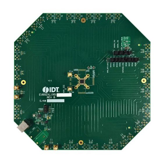
Board Overview
Use
Figure 1
and
Table 1
to identify: USB connector, input and output frequency SMA connectors.
Figure 1. Evaluation Board Overview
1
2
©2018 Integrated Device Technology, Inc.
9ZXL1951D PCIe Clock Generator
Evaluation Board
8
3
7
4
1
User Guide
6
5
March 23, 2018
Advertisement
Table of Contents

Related Manuals for IDT 9ZXL1951D


Summary of Contents for IDT 9ZXL1951D
-
Page 1: Evaluation Board User Guide
Introduction The evaluation board is designed to help the customer evaluate the 9ZXL1951D. The device is programmable through an SMBus interface. This user guide details the board set and connection, as well as the companion GUI installation for communicating to the device. -
Page 2: Usb Power Supply
Name On-board Connector Label Function Used for power-up of the device and connection with a PC, and USB Interface for interaction with the IDT PCIe GUI. On-board USB to SMBus connection. Power LED Power from USB connector. SMBus Header External SMBus connection. - Page 3 Figure 3. FTDI CDM Drivers Executable File Window 4. Connect the 9ZXL1951D board to the computer using the supplied USB cable. Double-click on the application file ClockCtl.exe to start the PCIe GUI support application. The PCIe Clock/Buffer GUI main window appears (see Figure 4).
- Page 4 9ZXL1951D PCIe Clock Generator Evaluation Board User Guide Figure 4. PCIe Clock/Buffer GUI Main Window Table 2 for descriptions. ©2018 Integrated Device Technology, Inc. March 23, 2018...
- Page 5 9ZXL1951D PCIe Clock Generator Evaluation Board User Guide Table 2. PCIe Clock/Buffer GUI Main Window Label Descriptions Label # Name Description Slave Address/TypeXfer The address is 7-bit slave address combined with “0” in LSB. For example, if the slave address is 1101000, “D0”...
- Page 6 9ZXL1951D PCIe Clock Generator Evaluation Board User Guide Table 2. PCIe Clock/Buffer GUI Main Window Label Descriptions (Cont.) Label # Name Description ▪ Read operation Register Operations Clicking the Read button initiates a read. If a chipset is used for reading, the byte count is determined by the value in the device byte count register.
- Page 7 9ZXL1951D PCIe Clock Generator Evaluation Board User Guide Table 2. PCIe Clock/Buffer GUI Main Window Label Descriptions (Cont.) Label # Name Description Write Register File to Clicking the “Write Register File to Device” button writes the register from file.A pop-up a window Device appears allowing the selection of the file path and the file name.
- Page 8 9ZXL1951D PCIe Clock Generator Evaluation Board User Guide Table 2. PCIe Clock/Buffer GUI Main Window Label Descriptions (Cont.) Label # Name Description Save Register’s Value Clicking the “Save Registers Value to File” button saves the registers to the file, A pop-up window is to File displayed.
- Page 9 9ZXL1951D PCIe Clock Generator Evaluation Board User Guide Table 2. PCIe Clock/Buffer GUI Main Window Label Descriptions (Cont.) Label # Name Description Byte Count Range A 32-byte value is the default display. If the byte count exceeds 32, select the radio button that Switch coincides with the new range.
- Page 10 9ZXL1951D PCIe Clock Generator Evaluation Board User Guide Clicking the “Save Registers Value to File” button saves the registers to a file. A pop-up window is displayed (see Figure 6). Select the file path and enter a file name, then click “Save”. The GUI will dump all register’s value then save to the file.
- Page 11 9ZXL1951D PCIe Clock Generator Evaluation Board User Guide Schematics Figure 7. 9ZXL1951D Connections ©2018 Integrated Device Technology, Inc. March 23, 2018...
- Page 12 9ZXL1951D PCIe Clock Generator Evaluation Board User Guide Figure 8. USB Interface and Power ©2018 Integrated Device Technology, Inc. March 23, 2018...
-
Page 13: Ordering Information
IDT or any third parties. IDT's products are not intended for use in applications involving extreme environmental conditions or in life support systems or similar devices where the failure or malfunction of an IDT product can be rea- sonably expected to significantly affect the health or safety of users.
Need help?
Do you have a question about the 9ZXL1951D and is the answer not in the manual?
Questions and answers