Advertisement
Quick Links
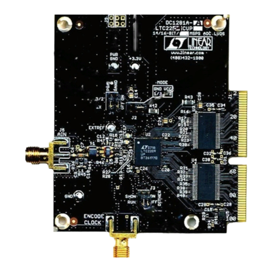
DESCRIPTION
Demonstration circuit 1281A supports a family of 16-
bit 160Msps/180Msps/185Msps ADCs. Each assem-
bly features one of the following devices: LTC
LTC2209#3BC, or LTC2209#3CD high speed, high dynamic
range ADC.
Other members of this family include the LTC2208 which
is a 130Msps 16-bit version of this device. The LTC2208 is
supported on the DC854 (CMOS) and the DC996 (LVDS).
Lower speed, single-ended clock versions are also sup-
ported on the DC918 and DC919.
Table 1. DC1281A Variants
DC1281A VARIANTS
ADC PART NUMBER
1281A-A
1281A-B
1281A-E
LTC2209#3BCPBF
1281A-F
LTC2209#3BCPBF
1281A-G
LTC2209#3CDPBF
1281A-H
LTC2209#3CDPBF
PERFORMANCE SUMMARY
PARAMETER
Supply Voltage – LTC2209
Supply Voltage – LTC2209#3BC
and LTC2209#3CD
Analog Input Range
Logic Input Voltages
Logic Output Voltages (Differential) Nominal Logic Levels (100Ω Load)
Sampling Frequency (Convert
Clock Frequency)
Convert Clock Level
Resolution
Input Frequency Range
SFDR
SNR
®
2209,
RESOLUTION
LTC2209
16-Bit
LTC2209
16-Bit
16-Bit
16-Bit
16-Bit
16-Bit
(T
= 25°C)
A
CONDITION
Depending on Sampling Rate and the A/D Converter Provided, This Supply Must
Provide Up to 700mA.
Depending on Sampling Rate and the A/D Converter Provided, This Supply Must
Provide Up to 700mA.
Depending on PGA Pin Voltage
Minimum Logic High
Maximum Logic Low
Minimum Logic Levels (100Ω Load)
See Table 1
50Ω Source Impedance, AC-Coupled or Ground Referenced (Convert Clock Input Is
Capacitor Coupled on Board and Terminated with 50Ω).
See Table 1
See Table 1
See Applicable Data Sheet
See Applicable Data Sheet
DEMO MANUAL DC1281A
16-Bit, 160Msps/180Msps/
Several versions of the 1281A demo board supporting
the LTC2209 16-bit series of A/D converters are listed in
Table 1. Depending on the required resolution, sample rate
and input frequency, the DC1281A is supplied with the
appropriate ADC and with an optimized input circuit. The
circuitry on the analog inputs is optimized for analog input
frequencies below 80MHz or from 80MHz to 160MHz. For
higher input frequencies, contact the factory for support.
Design files for this circuit board are available at
http://www.linear.com/demo
L, LT, LTC, LTM, Linear Technology and the Linear logo are registered trademarks; QuikEval
and PScope are trademarks of Linear Technology Corporation. All other trademarks are the
property of their respective owners.
MAXIMUM SAMPLE RATE
INPUT FREQUENCY
160Msps
1MHz to 80MHz
160Msps
80MHz to 160MHz
180Msps
1MHz to 80MHz
180Msps
80MHz to 160MHz
185Msps
1MHz to 80MHz
185Msps
80MHz to 160MHz
LTC2209
185Msps ADCs
SUPPLY VOLTAGE
3.3V
3.3V
3.6V
3.6V
3.6V
3.6V
VALUE
Optimized for 3.3V
[3.15V⇔3.45V min/max]
Optimized for 3.6V
[3.5V⇔3.78V min/max]
1.5V
to 2.25V
P-P
P-P
2V
0.8V
350mV/2.1V Common Mode
247mV/2.1V Common Mode
⇔2.5V
2V
Sine Wave or
P-P
P-P
Square wave
dc1281af
1
Advertisement

Related Manuals for Linear Technology DC1281A


Summary of Contents for Linear Technology DC1281A
- Page 1 Design files for this circuit board are available at ported on the DC918 and DC919. http://www.linear.com/demo L, LT, LTC, LTM, Linear Technology and the Linear logo are registered trademarks; QuikEval and PScope are trademarks of Linear Technology Corporation. All other trademarks are the property of their respective owners.
-
Page 2: Quick Start Procedure
Demonstration circuit 1281A is easy to set up to evaluate DC1281A Demonstration Circuit Board Jumpers the performance of the LTC2209 A/D converters. Refer to The DC1281A demonstration circuit board should have Figure 1 for proper measurement equipment setup and the following jumper settings as default: (as per Figure 1): follow the procedure below: J2: Mode (VCC) 2’s Complement DCS Off... - Page 3 Demonstration Circuit Note: This is not a logic-compatible input. It is terminated If a DC890 is used to acquire data from the DC1281A, the with 50Ω. Apply an encode clock to the SMA connector DC890 must first be connected to a powered USB port on the DC1281A demonstration circuit board marked J7 ENCODE INPUT.
-
Page 4: Parts List
DEMO MANUAL DC1281A QUICK START PROCEDURE Manual configuration settings: If the DC1281A demonstration circuit is properly connected to the DC890, PScope should automatically detect the Bits: 16 DC1281A, and configure itself accordingly. If necessary Alignment: 16 the procedure below explains how to manually configure PScope. - Page 5 DEMO MANUAL DC1281A PARTS LIST ITEM REFERENCE PART DESCRIPTION MANUFACTURER/PART NUMBER RES~100Ω~1%~1/16W~0603 VISHAY, CRCW0603100RFKEA R13, R16-R23, R30-R35, R38-R41 RES~100Ω~5%~1/20~0201 ACC/CR20-101JM R6-8, R14 RES~1k~1%~1/16W~0603 VISHAY, CRCW06031K00FKEA RES~100k~1%~1/16~0402 VISHAY, CRCW0402100KFKED R1, R2 RES~49.9Ω~1%~1/16~0402 VISHAY, CRCW040249R9FKED R3 (OPTION) RES~100Ω~1%~1/16W~0603 AAC/CR16-1000FM R11-R12,R46-R47 RES~68.1Ω~1%~1/16~0402 VISHAY, CRCW040268R1FKED R25, R26, R29 RES~4990Ω~1%~1/16~0402...
- Page 6 DEMO MANUAL DC1281A PARTS LIST ITEM REFERENCE PART DESCRIPTION MANUFACTURER/PART NUMBER DC1281A-E DC1281A GENERAL BOM CAP~NPO~4.7pF~50V~0.25pF~0402 AVX/04025A4R7CAT2A C9-C10 CAP~NPO~8.2pF~50V~0.25pF~0402 AVX/04025A8R2CAT2A IND~56nH~5%~0603 MURATA/LQP18MN56NG02D R36, R44 RES~86.6Ω~1%~1/16W~0603 VISHAY, CRCW060386R6FKEA RES~86.6Ω~1%~1/16~0402 VISHAY, CRCW040286R6FKED BALUN~RF~SMT~1:1 M/A-COM, MABA-007159-000000 (PbF) XFRM~RF~SMT~1:1CT M/A-COM, MABAES0060 (PbF) ADC~16-BIT~180MSPS LINEAR/LTC2209CUP#3BCPBF...
-
Page 7: Schematic Diagram
Information furnished by Linear Technology Corporation is believed to be accurate and reliable. However, no responsibility is assumed for its use. Linear Technology Corporation makes no representa- tion that the interconnection of its circuits as described herein will not infringe on existing patent rights. - Page 8 Linear Technology Corporation (LTC) provides the enclosed product(s) under the following AS IS conditions: This demonstration board (DEMO BOARD) kit being sold or provided by Linear Technology is intended for use for ENGINEERING DEVELOPMENT OR EVALUATION PURPOSES ONLY and is not provided by LTC for commercial use. As such, the DEMO BOARD herein may not be complete in terms of required design-, marketing-, and/or manufacturing-related protective considerations, including but not limited to product safety measures typically found in finished commercial goods.
- Page 9 Mouser Electronics Authorized Distributor Click to View Pricing, Inventory, Delivery & Lifecycle Information: Analog Devices Inc. DC1281A-B DC1281A-A...
Need help?
Do you have a question about the DC1281A and is the answer not in the manual?
Questions and answers