Advertisement
Quick Links
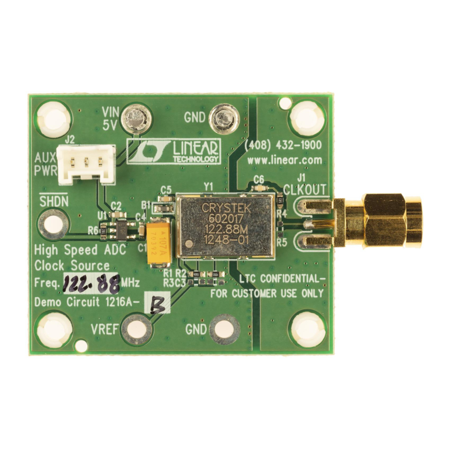
Description
Demonstration circuit 1216 is a low jitter, low noise clock
source for demonstrating high speed ADCs. Each assem-
bly includes a LDO regulator and a high precision VCXO.
Functionally, this circuit uses a linear regulator to provide
a clean 5V to a VCXO at a fixed frequency. This VCXO is
capable of providing a signal which is clean enough to
produce data sheet performance from high speed ADCs.
It is designed to have 50Ω output impedance, but has
provision for other termination resistors if needed.
Table 1. DC1216A Variants
DC1216A VARIANTS
DC1216A-A
DC1216A-B
DC1216A-C
DC1216A-D
Note: DC1216A-A, DC1216A-B and DC1216A-C are optimized to be used
with the data converter demo boards. The DC1216A-D is optimized to
drive the synthesizer demo boards.
Arrow.com.
Downloaded from
VCXO PART NUMBER
OUTPUT FREQUENCY
Crystek 601964
100MHz
Crystek 602017
122.88MHz
Crystek 602019
80MHz
Crystek 601964
100MHz
DEMO MANUAL DC1216
High Speed ADC
This circuit also is a model for the clock source of ADCs.
It shows how to properly implement a VCXO correctly to
drive the clock of an ADC. It can be used with a DC1075
to produce lower clock frequencies.
Design files for this circuit board are available at
http://www.linear.com/demo
L, LT, LTC, LTM, Linear Technology and the Linear logo are registered trademarks of Linear
Technology Corporation. All other trademarks are the property of their respective owners.
Clock Source
dc1216f
1
Advertisement

Related Manuals for Linear Technology DC1216A-A


Summary of Contents for Linear Technology DC1216A-A
- Page 1 ADCs. L, LT, LTC, LTM, Linear Technology and the Linear logo are registered trademarks of Linear It is designed to have 50Ω output impedance, but has Technology Corporation. All other trademarks are the property of their respective owners.
-
Page 2: Quick Start Procedure
DEMO MANUAL DC1216 Quick start proceDure SETUP 5V TO 9V The DC1216 requires an external voltage of 5V. This volt- age can be as high as 9V. The SMA connector should be connected to the ADC directly, or through a clock divider OUTPUT FREQUENCY circuit such as the DC1075A. -
Page 3: Parts List
R1, R2 RES, CHIP, 4.99k, 1/10W, 1% 0603 VISHAY, CRCW06034K99FKEA R3, R5 (OPT) RES, 0603 RES, CHIP, 1k, 1/10W, 5% 0603 VISHAY, CRCW06031K00JNEA IC LT1761ES5-3.3, SOT23-S5 LINEAR TECHNOLOGY, LT1761ES5-3.3#PBF (STAND-OFF) STAND-OFF, NYLON 0.25" KEYSTONE, 8831(SNAP ON) STENCIL STENCIL 1216A dc1216f Arrow.com. - Page 4 DEMO MANUAL DC1216 parts List DEMO BOARD 1216-A ITEM REFERENCE PART DESCRIPTION MANUFACTURER/PART NUMBER DC1216A DC1216A GENERAL BOM GENERAL BOM CRYSTAL 601964 CRYSTEK, 601964 RES, CHIP, 5.1Ω, 1/10W, 5% 0603 VISHAY, CRCW06035R10JNEA FAB, PRINTED CIRCUIT BOARD DEMO CIRCUIT 1216A DEMO BOARD 1216-B ITEM REFERENCE PART DESCRIPTION...
-
Page 5: Schematic Diagram
Information furnished by Linear Technology Corporation is believed to be accurate and reliable. However, no responsibility is assumed for its use. Linear Technology Corporation makes no representa- tion that the interconnection of its circuits as described herein will not infringe on existing patent rights. - Page 6 Linear Technology Corporation (LTC) provides the enclosed product(s) under the following AS IS conditions: This demonstration board (DEMO BOARD) kit being sold or provided by Linear Technology is intended for use for ENGINEERING DEVELOPMENT OR EVALUATION PURPOSES ONLY and is not provided by LTC for commercial use. As such, the DEMO BOARD herein may not be complete in terms of required design-, marketing-, and/or manufacturing-related protective considerations, including but not limited to product safety measures typically found in finished commercial goods.
Need help?
Do you have a question about the DC1216A-A and is the answer not in the manual?
Questions and answers