
Subscribe to Our Youtube Channel
Related Manuals for Fibocom NL668-AM Series


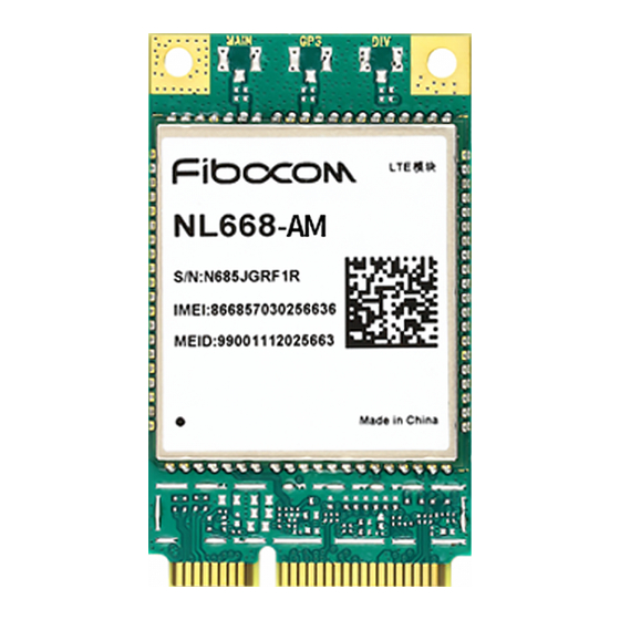
Summary of Contents for Fibocom NL668-AM Series
- Page 1 FIBOCOM NL668-AM Hardware User Manual Version: V1.0.1 Date: 2018-11-13 Reproduction forbidden without Fibocom Wireless Inc. written authorization - All Rights Reserved. FIBOCOM NL668-AM Hardware User Manual Page 1 of 62...
- Page 2 Product model Description MCP is 4+2, and supports MAIN_ANT, DIV_ANT, GNSS_ANT NL668-AM-00 Based on NL668-AM-00 delete Band 71 NL668-AM-01 Reproduction forbidden without Fibocom Wireless Inc. written authorization - All Rights Reserved. FIBOCOM NL668-AM Hardware User Manual Page 2 of 62...
- Page 3 Assessor Approver Description Date V1.0.0 2018-10-26 Initial version Gaoying Chenguojiang Tumin V1.0.1 2018-11-13 Add Band 17 Gaoying Chenguojiang Tumin Reproduction forbidden without Fibocom Wireless Inc. written authorization - All Rights Reserved. FIBOCOM NL668-AM Hardware User Manual Page 3 of 62...
-
Page 4: Table Of Contents
UART Interface ......................34 3.6.1 UART interface definition ....................34 3.6.2 UART port application ....................35 Status Indicator ......................36 Reproduction forbidden without Fibocom Wireless Inc. written authorization - All Rights Reserved. FIBOCOM NL668-AM Hardware User Manual Page 4 of 62... - Page 5 SMT Patch ........................53 Appendix A Terms and Acronyms ................... 54 Appendix B ADP & MiniPCIe RF ports trace………………………………………………... 57 Reproduction forbidden without Fibocom Wireless Inc. written authorization - All Rights Reserved. FIBOCOM NL668-AM Hardware User Manual Page 5 of 62...
- Page 6 Figure 6-1Module Product Appearance (Top) ..................52 Figure 6-2 Module Product Appearance (Bottom) ................52 Figure 6-3 Dimension of Structure (Unit: mm) ..................53 Reproduction forbidden without Fibocom Wireless Inc. written authorization - All Rights Reserved. FIBOCOM NL668-AM Hardware User Manual Page 6 of 62...
- Page 7 Table 5-3 Electrical Characteristics of the Interface in Operating Status ........... 50 Table 5-4 Environmental Reliability Requirements ................50 Table 5-5 ESD Allowable Discharge Range ..................51 Reproduction forbidden without Fibocom Wireless Inc. written authorization - All Rights Reserved. FIBOCOM NL668-AM Hardware User Manual Page 7 of 62...
- Page 8 Table A-0-1 Terms and Acronyms ....................... 56 Reproduction forbidden without Fibocom Wireless Inc. written authorization - All Rights Reserved. FIBOCOM NL668-AM Hardware User Manual Page 8 of 62...
-
Page 9: Foreword
Product manufacturers need to communicate the following safety instructions to end users. In case of failure to comply with these safety rules, Fibocom will not be responsible for the consequences caused by the user’s misuse. -
Page 10: Reference Standards
3GPP TS 27.005 V10.0.1: Use of Data Terminal Equipment - Data Circuit terminating Equipment (DTE - DCE) interface for Short Message Service (SMS) and Cell Broadcast Service (CBS) Reproduction forbidden without Fibocom Wireless Inc. written authorization - All Rights Reserved. FIBOCOM NL668-AM Hardware User Manual... -
Page 11: Related Document
FCC radio frequency exposure limits, human proximity to the antenna shall not be less than 20cm (8 inches) during normal operation. Reproduction forbidden without Fibocom Wireless Inc. written authorization - All Rights Reserved. FIBOCOM NL668-AM Hardware User Manual... - Page 12 Operation is subject to the following two conditions: (1) this device may not cause harmful interference and (2) this device must accept any interference received, including interference that may cause undesired operation. Reproduction forbidden without Fibocom Wireless Inc. written authorization - All Rights Reserved. FIBOCOM NL668-AM Hardware User Manual Page 12 of 62...
-
Page 13: Product Overview
Weight: About 5.5g Interface Antenna: Main x 1, GNSS x 1, DIV x 1 Antenna USIM 3.0V/1.8V Functional Reproduction forbidden without Fibocom Wireless Inc. written authorization - All Rights Reserved. FIBOCOM NL668-AM Hardware User Manual Page 13 of 62... -
Page 14: Hardware Diagram
UMTS/ LTE FDD controller PMIC UART、USB、SIM、PCM、I2C、SPI、SGMII、SDIO、ADC RF includes: RF Transceiver RF PA RF filter Antenna Reproduction forbidden without Fibocom Wireless Inc. written authorization - All Rights Reserved. FIBOCOM NL668-AM Hardware User Manual Page 14 of 62... -
Page 15: Figure 2-1 Hardware Diagram
Figure 2-1 Hardware Diagram Reproduction forbidden without Fibocom Wireless Inc. written authorization - All Rights Reserved. FIBOCOM NL668-AM Hardware User Manual Page 15 of 62... -
Page 16: Application Interface
“73 ~ 112” is the thermal pin, and the module is grounded internally. It is recommended that the heat sink pad is reserved for PCB packaging and welded. Reproduction forbidden without Fibocom Wireless Inc. written authorization - All Rights Reserved. FIBOCOM NL668-AM Hardware User Manual... -
Page 17: Pin Definition
USIM_PRESENCE USIM card hot plug detection min=1.2V max=2.0V For 1.8V USIM: USIM _VDD Vmax=1.9V USIM power Vmin=1.7V Reproduction forbidden without Fibocom Wireless Inc. written authorization - All Rights Reserved. FIBOCOM NL668-AM Hardware User Manual Page 17 of 62... - Page 18 Turn on/off the module, active low, no PWRKEY min=1.3V need pull up externally max=0.5V Ground SD_INS_DET Reserved PCM_IN min=-0.3V PCM input signal Reproduction forbidden without Fibocom Wireless Inc. written authorization - All Rights Reserved. FIBOCOM NL668-AM Hardware User Manual Page 18 of 62...
- Page 19 OD - I2C interface data signal ADC1 Analog to digital converter interface ADC0 Analog to digital converter interface 0 Ground Reproduction forbidden without Fibocom Wireless Inc. written authorization - All Rights Reserved. FIBOCOM NL668-AM Hardware User Manual Page 19 of 62...
- Page 20 Module output data carrier detection min=1.35V min=-0.3V max=0.6V Clear to send min=1.2V max=2.0V max=0.45V Request to send min=1.35V min=-0.3V max=0.6V Data ready min=1.2V Reproduction forbidden without Fibocom Wireless Inc. written authorization - All Rights Reserved. FIBOCOM NL668-AM Hardware User Manual Page 20 of 62...
- Page 21 Reserved SGMII_MDATA Reserved SGMII_MCLK Reserved SGMII_TX_M Reserved SGMII_TX_P Reserved SGMII_RX_P Reserved SGMII_RX_M Reserved PM_ENABLE Reserved VREG_L5_UIM2 Reserved SDC1_DATA_3 Reserved Reproduction forbidden without Fibocom Wireless Inc. written authorization - All Rights Reserved. FIBOCOM NL668-AM Hardware User Manual Page 21 of 62...
-
Page 22: Power Supply
0-54,56,72-112 Table 3-2 Power Interfaces Note: In the rest of the document, VBAT_BB, VBAT_RF will be replaced with VBAT. Reproduction forbidden without Fibocom Wireless Inc. written authorization - All Rights Reserved. FIBOCOM NL668-AM Hardware User Manual Page 22 of 62... -
Page 23: Power Supply
3.3V. Otherwise, the module may power off or restart. The power limit is shown in Figure 3-3: Reproduction forbidden without Fibocom Wireless Inc. written authorization - All Rights Reserved. FIBOCOM NL668-AM Hardware User Manual Page 23 of 62... -
Page 24: Output
Paging cycle #256 frames Idle ≤15 Radio Off AT+CFUN=4 ≤3 DRX=6 ≤3 DRX=7 sleep WCDMA ≤3 DRX=8 ≤3 DRX=9 Reproduction forbidden without Fibocom Wireless Inc. written authorization - All Rights Reserved. FIBOCOM NL668-AM Hardware User Manual Page 24 of 62... -
Page 25: Control Signal
When module is in power off mode , give it a Tst (100ms~2s) low level, PWRKEY and then pull it high, the module will power on; When module is in power Reproduction forbidden without Fibocom Wireless Inc. written authorization - All Rights Reserved. FIBOCOM NL668-AM Hardware User Manual Page 25 of 62... -
Page 26: Module Power On
(recommended:ESD9X5VL-2/TR) near the button for ESD protection. The reference circuit is shown in Figure 3-5. Figure 3-5 Button Power on Reference Circuit Reproduction forbidden without Fibocom Wireless Inc. written authorization - All Rights Reserved. FIBOCOM NL668-AM Hardware User Manual Page 26 of 62... -
Page 27: Module Power Off
3.3.2.1 Power off Timing 1. When the module is working properly, do not cut off the power of the module immediately to avoid Reproduction forbidden without Fibocom Wireless Inc. written authorization - All Rights Reserved. FIBOCOM NL668-AM Hardware User Manual... -
Page 28: Module Reset
Refer to Figure 3-8 reset circuit. It is similar to the PWRKEY control circuit. The client can control the RESET_N pin using an OC/OD drive circuit or push button. Reproduction forbidden without Fibocom Wireless Inc. written authorization - All Rights Reserved. FIBOCOM NL668-AM Hardware User Manual... -
Page 29: Figure 3-8 Reset_N Oc/Od Drive Reference Circuit
Another reset control is shown in Figure 3-9. Figure 3-9 RESET_N Button Reference Circuit 3.3.3.2 RESET control Timing Figure 3-10 Reset Control Timing Reproduction forbidden without Fibocom Wireless Inc. written authorization - All Rights Reserved. FIBOCOM NL668-AM Hardware User Manual Page 29 of 62... -
Page 30: Usb Interface
USB_DM and USB_DP signal cables are routed on the signal layer closest to the ground layer, and the cables shall be grounded; Reproduction forbidden without Fibocom Wireless Inc. written authorization - All Rights Reserved. FIBOCOM NL668-AM Hardware User Manual... -
Page 31: Usim Interface
3.5.2 USIM interface circuit 3.5.2.1 SIM card slot with detection signal USIM/SIM design requires the use of SIM card slot (Fibocom recommend: SIM016-8P-220P). We recommend using hot plug slot with SIM_DECTECT function. Reproduction forbidden without Fibocom Wireless Inc. written authorization - All Rights Reserved. -
Page 32: Figure 3-11 Sim Card Slot Diagram Sim016-8P-220P
SIM card is insert, USIM_PRESENCE pin is high level SIM card is no insert, USIM_PRESENCE pin is low level Reproduction forbidden without Fibocom Wireless Inc. written authorization - All Rights Reserved. FIBOCOM NL668-AM Hardware User Manual Page 32 of 62... -
Page 33: Usim Hot Plug
After reading the SIM card information, the module will register network. When the USIM_PRESENCE is in low level, the module detects that the SIM card is removed, then it will not read the SIM card. Reproduction forbidden without Fibocom Wireless Inc. written authorization - All Rights Reserved. FIBOCOM NL668-AM Hardware User Manual... -
Page 34: Usim Design Requirements
The following table describes the main serial port pin. Pin name Description Ring indicator Data carrier detection Clear to send Reproduction forbidden without Fibocom Wireless Inc. written authorization - All Rights Reserved. FIBOCOM NL668-AM Hardware User Manual Page 34 of 62... -
Page 35: Uart Port Application
The input and output circuit design in the following dashed part can refer to that in the solid line part, but pay attention to the connection direction. Reproduction forbidden without Fibocom Wireless Inc. written authorization - All Rights Reserved. FIBOCOM NL668-AM Hardware User Manual... -
Page 36: Status Indicator
Request SIM PIN Flash (600ms High/600ms Low) Registering network (T<15S) Register network failed Slow flash (75ms Low /3000ms High) Standby Reproduction forbidden without Fibocom Wireless Inc. written authorization - All Rights Reserved. FIBOCOM NL668-AM Hardware User Manual Page 36 of 62... -
Page 37: Low Power Mode
AT+CFUN=0,0--enter the flight mode AT command control AT+CFUN=1,0--enter the normal mode Table 3-18 Module enter Fly Mode Reproduction forbidden without Fibocom Wireless Inc. written authorization - All Rights Reserved. FIBOCOM NL668-AM Hardware User Manual Page 37 of 62... -
Page 38: Sleep Mode
( X=0,high level active to sleep; X=1,low level active to sleep) AT+CSCLK = 1 command to enable sleep function. AT+GTUSBSLEEPEN=0,0 command to set USB sleep mode Reproduction forbidden without Fibocom Wireless Inc. written authorization - All Rights Reserved. FIBOCOM NL668-AM Hardware User Manual Page 38 of 62... - Page 39 Wake up the module by send the AT command fast. Note: Since the level of UART sleep power is different, power dissipation when use ATS24 command Reproduction forbidden without Fibocom Wireless Inc. written authorization - All Rights Reserved. FIBOCOM NL668-AM Hardware User Manual Page 39 of 62...
-
Page 40: Digital Audio Interface Pcm
Table 3-21 PCM Interface Description NL668-AM adopts the above configuration by default, if you need to make adjustment, please contact our Reproduction forbidden without Fibocom Wireless Inc. written authorization - All Rights Reserved. FIBOCOM NL668-AM Hardware User Manual Page 40 of 62... -
Page 41: Pcm Signal Description
2.048MHz clock in 16bit linear format encoding. PCM_SYNC is a 8kHz burst (488nS). Figure 3-17 PCM_SYNC Timing Figure 3-18 PCM_CODEC to NL668-AM Timing Figure 3-19 NL668-AM to PCM_CODEC Timing Reproduction forbidden without Fibocom Wireless Inc. written authorization - All Rights Reserved. FIBOCOM NL668-AM Hardware User Manual Page 41 of 62... -
Page 42: Adc Function
Description ADC0 Analog to digital converter interface 0 ADC1 Analog to digital converter interface 1 Table 3-22 ADC Interface Reproduction forbidden without Fibocom Wireless Inc. written authorization - All Rights Reserved. FIBOCOM NL668-AM Hardware User Manual Page 42 of 62... -
Page 43: Rf Interface
Band 66 23±1 10MHz Bandwidth, 1 RB Band 71 23±1 10MHz Bandwidth, 1 RB Table 4-2 RF Output Power Reproduction forbidden without Fibocom Wireless Inc. written authorization - All Rights Reserved. FIBOCOM NL668-AM Hardware User Manual Page 43 of 62... -
Page 44: Rf Receiving Sensitivity Of Nl668-Am
Condition Typ. GNSS fixing 68mA Current consumption 68mA GNSS tracking (AT+CFUN=0) 33mA Standby Cold start TTFF GNSS Warm start Reproduction forbidden without Fibocom Wireless Inc. written authorization - All Rights Reserved. FIBOCOM NL668-AM Hardware User Manual Page 44 of 62... -
Page 45: Rf Pcb Design
Figure 4-1 is the reference circuit design for the main and diversity antenna. These matches need to be placed close to the antenna: MAIN Antenna Module Antenna ANT_MAIN ANT_DIV Figure 4-1RF Reference Circuit Design Reproduction forbidden without Fibocom Wireless Inc. written authorization - All Rights Reserved. FIBOCOM NL668-AM Hardware User Manual Page 45 of 62... -
Page 46: Antenna Design
S11 shows that the matching degree of the antenna’s 50 ohm impedance, to a certain extent, affects the antenna efficiency. VSWR test methods can be used to measure this parameter. Recommend S11 <-10dB. Reproduction forbidden without Fibocom Wireless Inc. written authorization - All Rights Reserved. FIBOCOM NL668-AM Hardware User Manual Page 46 of 62... - Page 47 LTE band 17(700): 42 MHz LTE band 13(700): 41 MHz LTE Band 66(1700): 470MHz LTE band 71(600): 81MHz Impedance 50 ohms Reproduction forbidden without Fibocom Wireless Inc. written authorization - All Rights Reserved. FIBOCOM NL668-AM Hardware User Manual Page 47 of 62...
-
Page 48: Table 4-5 Main Antenna Requirement
Frequency range: 1559MHz~1607MHz Polarization type: right-circular or linear polarization GNSS VSWR::< 2(Type) Passive antenna gain:> 0dBi Table 4-5 Main Antenna Requirement Reproduction forbidden without Fibocom Wireless Inc. written authorization - All Rights Reserved. FIBOCOM NL668-AM Hardware User Manual Page 48 of 62... -
Page 49: Electrical Characteristics
Table 5-2Environment Temperature Range 5.3 Electrical characteristics of the interface in operating status : logic low level; : logic high level; Reproduction forbidden without Fibocom Wireless Inc. written authorization - All Rights Reserved. FIBOCOM NL668-AM Hardware User Manual Page 49 of 62... -
Page 50: Environmental Reliability Requirements
(20Hz), other -3dB/octave Connector life test 30 times of insertion/removal for RF antenna interface cable Table 5-4 Environmental Reliability Requirements Reproduction forbidden without Fibocom Wireless Inc. written authorization - All Rights Reserved. FIBOCOM NL668-AM Hardware User Manual Page 50 of 62... -
Page 51: Esd Characteristics
Contact discharge VBAT,GND ±10KV ±5KV Antenna interface ±8KV ±4KV Other interface ±1KV ±0.5KV Table 5-5 ESD Allowable Discharge Range Reproduction forbidden without Fibocom Wireless Inc. written authorization - All Rights Reserved. FIBOCOM NL668-AM Hardware User Manual Page 51 of 62... -
Page 52: Structure Specification
The product appearance for NL668-AM module is shown in Figure 6-1 and 6-2: Figure 6-1Module Product Appearance (Top) Figure 6-2 Module Product Appearance (Bottom) Reproduction forbidden without Fibocom Wireless Inc. written authorization - All Rights Reserved. FIBOCOM NL668-AM Hardware User Manual Page 52 of 62... -
Page 53: Dimension Of Structure
Figure 6-3 Dimension of Structure (Unit: mm) 6.3 SMT Patch For module stencil design, please refer to FIBOCOM_ NL668 LCC SMT Application Design Instruction. Reproduction forbidden without Fibocom Wireless Inc. written authorization - All Rights Reserved. FIBOCOM NL668-AM Hardware User Manual Page 53 of 62... -
Page 54: Appendix A Terms And Acronyms
Secondary Cell for CA Mobile Equipment Mobile Station Mobile Terminated Printed Circuit Board Protocol Data Unit Phase Shift Keying Reproduction forbidden without Fibocom Wireless Inc. written authorization - All Rights Reserved. FIBOCOM NL668-AM Hardware User Manual Page 54 of 62... - Page 55 Maximum Input High Level Voltage Value IHmax Minimum Input High Level Voltage Value IHmin Maximum Input Low Level Voltage Value ILmax Reproduction forbidden without Fibocom Wireless Inc. written authorization - All Rights Reserved. FIBOCOM NL668-AM Hardware User Manual Page 55 of 62...
- Page 56 Minimum Output Low Level Voltage Value OLmin VSWR Voltage Standing Wave Ratio WCDMA Wideband Code Division Multiple Access Table A-0-1 Terms and Acronyms Reproduction forbidden without Fibocom Wireless Inc. written authorization - All Rights Reserved. FIBOCOM NL668-AM Hardware User Manual Page 56 of 62...
-
Page 57: Appendix B Adp & Minipcie Rf Ports Trace
Appendix B ADP & MiniPCIe RF ports trace NL668-AM MiniPCIe a) Primary Antenna Reproduction forbidden without Fibocom Wireless Inc. written authorization - All Rights Reserved. FIBOCOM NL668-AM Hardware User Manual Page 57 of 62... - Page 58 Diversity Antenna Reproduction forbidden without Fibocom Wireless Inc. written authorization - All Rights Reserved. FIBOCOM NL668-AM Hardware User Manual Page 58 of 62...
- Page 59 GNSS Antenna Reproduction forbidden without Fibocom Wireless Inc. written authorization - All Rights Reserved. FIBOCOM NL668-AM Hardware User Manual Page 59 of 62...
- Page 60 NL668-AM ADP a) Primary Antenna Reproduction forbidden without Fibocom Wireless Inc. written authorization - All Rights Reserved. FIBOCOM NL668-AM Hardware User Manual Page 60 of 62...
- Page 61 Diversity Antenna Reproduction forbidden without Fibocom Wireless Inc. written authorization - All Rights Reserved. FIBOCOM NL668-AM Hardware User Manual Page 61 of 62...
- Page 62 GNSS Antenna Reproduction forbidden without Fibocom Wireless Inc. written authorization - All Rights Reserved. FIBOCOM NL668-AM Hardware User Manual Page 62 of 62...
Need help?
Do you have a question about the NL668-AM Series and is the answer not in the manual?
Questions and answers