
Related Manuals for EPC EPC9085


Summary of Contents for EPC EPC9085
- Page 1 Development Board EPC9085 Quick Start Guide 40 V Half-bridge with Gate Drive, Using EPC2049...
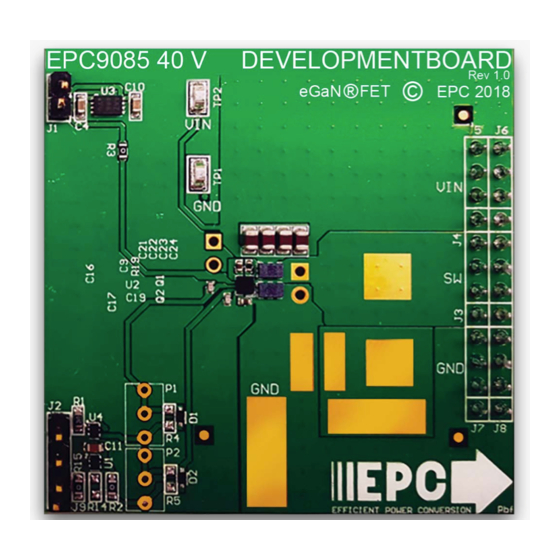
- Page 2 QUICK START GUIDE EPC9085 DESCRIPTION The EPC9085 development board is a 40 V maximum device voltage, 20 A Table 1: Performance Summary (T = 25°C) EPC9085 maximum output current, half bridge with onboard gate drives, featuring Symbol Parameter Conditions Max Units the EPC2049 enhancement mode (eGaN®) field effect transistor (FET).
- Page 3 Logic and LM5113 dead-time PWM input gate adjust driver Figure 1: Block diagram of EPC9085 development board Gate drive supply (note polarity) supply Optional 2-pin 7.5 V – 12 V Half bridge configuration header for switch Optional...
- Page 4 EPC9085 THERMAL CONSIDERATIONS The EPC9085 development board showcases the EPC2049 eGaN NOTE. The EPC9085 development board does not have any current or thermal protection on board. FET. The EPC9085 is intended for bench evaluation with low ambient For more information regarding the thermal performance of EPC eGaN FETs, please temperature and convection cooling.
- Page 5 CON2 7 - 12 Vdc MCP1703 Keystone 5015 CON4 CON2 CON4 CON2 NC7SZ00L6X Zero Optional CON4 4.7 F NC7SZ08L6X SDM03U40 CON4 PWM2 Optional LM5113TM 100pF SDM03U40 CON2 Optional 100pF CON4 Zero Keystone 5015 CON4 CON2 Figure 4: EPC9085 - Schematic...
- Page 6 Demonstration Board Notification The EPC9085 board is intended for product evaluation purposes only and is not intended for commercial use. Replace components on the Evaluation Board only with those parts shown on the parts list (or Bill of Materials) in the Quick Start Guide. Contact an authorized EPC representative with any questions.
Need help?
Do you have a question about the EPC9085 and is the answer not in the manual?
Questions and answers