
Related Manuals for EPC EPC9084


Summary of Contents for EPC EPC9084
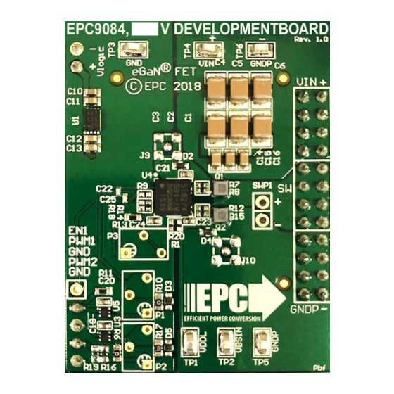
- Page 1 Development Board EPC9084 Quick Start Guide 350 V Half-Bridge with Gate Drive, Using EPC2050 Revision 1.0...
-
Page 2: Quick Start Procedure
QUICK START GUIDE EPC9084 DESCRIPTION Table 1: Performance Summary (T = 25°C) EPC9084 The EPC9084 development board, figure 1, is a 350 V maximum device Symbol Parameter Conditions Max Units voltage, 4 A maximum output current, half bridge with onboard gate Gate Drive Input Supply Range drives, featuring two EPC2050 enhancement mode (eGaN®) field effect... - Page 3 = 28 V, I = 4 A, f = 50 kHz, L = 440 H Buck Figure 4: Typical Waveform for the EPC9084 operating as a buck converter EPC – EFFICIENT POWER CONVERSION CORPORATION | WWW.EPC-CO.COM | COPYRIGHT 2018 |...
-
Page 4: Measurement Considerations
QUICK START GUIDE EPC9084 MEASUREMENT CONSIDERATIONS Please contact EPC for special instructions on using these connections. To prevent an unterminated transmission line hanging on the gate it The EPC9084 development board has been provided with is recommended to remove resistors R21 & R22 when not using this specially designed high frequency (up to 1 GHz minimum) capable feature. -
Page 5: Thermal Considerations
EPC9084 THERMAL CONSIDERATIONS The EPC9084 development board showcases the EPC2050 eGaN FET. The NOTE. The EPC9084 development board does not have any current or thermal protection on board. EPC9084 is intended for bench evaluation with typical room ambient temperature. The addition of heat-sinking and forced air cooling can... - Page 6 QUICK START GUIDE EPC9084 EPC – EFFICIENT POWER CONVERSION CORPORATION | WWW.EPC-CO.COM | COPYRIGHT 2018 |...
-
Page 7: Visit Our Website
Demonstration Board Notification The EPC9084 board is intended for product evaluation purposes only and is not intended for commercial use. Replace components on the Evaluation Board only with those parts shown on the parts list (or Bill of Materials) in the Quick Start Guide. Contact an authorized EPC representative with any questions.
Need help?
Do you have a question about the EPC9084 and is the answer not in the manual?
Questions and answers