Table of Contents
Advertisement
Quick Links
Warranty
All products manufactured by ICP DAS are warranted against defective materials for a
period of one year from the date of delivery to the original purchaser.
Warning
ICP DAS assume no liability for damages consequent to the use of this product. ICP
DAS reserves the right to change this manual at any time without notice. The information
furnished by ICP DAS is believed to be accurate and reliable. However, no responsibility is
assumed by ICP DAS for its use, nor for any infringements of patents or other rights of third
parties resulting from its use.
Copyright
Copyright 1997 by ICP DAS. All rights are reserved.
Trademark
The names used for identification only may be registered trademarks of their respective
companies.
License
The user can use, modify and backup this software
The user may not reproduce, transfer or distribute this software, or any copy, in whole or in
part.
A-812PG Hardware Manual (Ver.1.2, Sep/2005, IPH-004-12)
A-812PG
Hardware User's Manual
on a single machine.
----- 1
Advertisement
Table of Contents

Related Manuals for ICP DAS USA A-812PG


Summary of Contents for ICP DAS USA A-812PG
- Page 1 License on a single machine. The user can use, modify and backup this software The user may not reproduce, transfer or distribute this software, or any copy, in whole or in part. A-812PG Hardware Manual (Ver.1.2, Sep/2005, IPH-004-12) ----- 1...
-
Page 2: Table Of Contents
2.4.5 Clear Interrupt Request _________________________________________________________ 19 2.4.6 A/D Gain Control Register ______________________________________________________ 20 2.4.7 A/D Multiplex Control Register __________________________________________________ 21 2.4.8 A/D Mode Control Register _____________________________________________________ 21 2.4.8 A/D Software Trigger Control Register ____________________________________________ 23 A-812PG Hardware Manual (Ver.1.2, Sep/2005, IPH-004-12) ----- 2... - Page 3 2.11.2 DB-16P for Digital input_______________________________________________________ 34 2.11.3 DB-16R for Digital output _____________________________________________________ 34 Calibration___________________________________________________________ 35 3.1 Calibration VR Description ________________________________________________ 36 3.2 D/A Calibration Steps _____________________________________________________ 37 3.3 A/D Calibration Steps _____________________________________________________ 37 A-812PG Hardware Manual (Ver.1.2, Sep/2005, IPH-004-12) ----- 3...
-
Page 4: Introduction
The A-812PG is a high performance, multifunction analog, digital I/O board for the PC AT compatible computer. The A-812PG provides low gain (1, 2, 4, 8, 16). The A-812PG contains a 12-bit ADC with up to 16 single-ended analog inputs. The maximum sample rate of A/D converter is about 62.5K sample/sec. -
Page 5: Specifications
Channels : 16 single-ended Input range : (software programmable) A-812PG:bipolar : ±10V, ±5V, ±2.5V, ±1.25V, ±0.625V, ±0.3125V (input range : ±10V or ±0.3125V by Jumper JP4 selected ) Input current : 250 nA max (125 nA typical ) at 25 deg. -
Page 6: Da Converter
Settling time : 0.6 microseconds to 0.01% for full scale step 1.3.5 Digital I/O Output port : 16 bits, TTL compatible Input port : 16 bits, TTL compatible 1.3.6 Interrupt Channel Level : 3,4,5,6,7,9,10,11,12,14,15, jumper selectable Enable : Via control register A-812PG Hardware Manual (Ver.1.2, Sep/2005, IPH-004-12) ----- 6... -
Page 7: Programmable Timer/Counter
1.3.8 Direct Memory Access Channel (DMA) Level : CH1 or CH3, jumper selectable Enable : via DMA bit of control register Termination : by interrupt on T/C Transfer rate : 100K conversions/sec.(DOS Software manual, sec. 4.11) A-812PG Hardware Manual (Ver.1.2, Sep/2005, IPH-004-12) ----- 7... -
Page 8: Applications
If any of these items is missing or damaged, contact the dealer who provides you this product. Save the shipping materials and carton in case you want to ship or store the product in the future. A-812PG Hardware Manual (Ver.1.2, Sep/2005, IPH-004-12) ----- 8... -
Page 9: Hardware Configuration
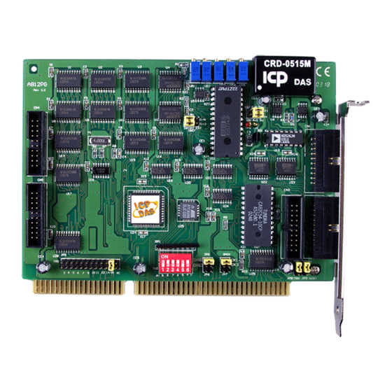
2. Hardware Configuration 2.1 Board Layout BB ADS-774 A-812PG Hardware Manual (Ver.1.2, Sep/2005, IPH-004-12) ----- 9... -
Page 10: I/O Base Address Setting
2.2 I/O Base Address Setting The A-812PG occupies 16 consecutive locations in I/O address space. The base address is set by DIP switch SW1. The default address is 0x220. SW1 : BASE ADDRESS BASE ADDR 200-20F 210-21F 220-22F( ) 230-23F... -
Page 11: Jumper Setting
: D/A voltage output = 0 to 5V (both channel) Select ( 10V) : D/A voltage output = 0 to 10V (both channel) JP3 is validate only if JP1/JP2 select D/A internal reference voltage A-812PG Hardware Manual (Ver.1.2, Sep/2005, IPH-004-12) ----- 11... -
Page 12: Jp1, Jp2 : D/A Int/Ext Ref Voltage Selection
(default) EXTTRG EXTTRG The A-812PG supports two trigger type, internal trigger and external trigger. The external trigger comes from ExtTrg, CN3 pin 1. There are two types of internal trigger, software trigger and pacer trigger. A-812PG Hardware Manual (Ver.1.2, Sep/2005, IPH-004-12) -
Page 13: Jp5 : Interrupt Level Selection
(default) 9 10 11 12 14 15 NC The interrupt channel can not be shared. The A-812PG software driver can support 8 different boards in one system but only 2 of these cards can use interrupt transfer function. A-812PG Hardware Manual (Ver.1.2, Sep/2005, IPH-004-12) -
Page 14: Jp9 : User Timer/Counter Clock Input Selection
(default) EXTCLK EXTCLK The A-812PG has 3 independent 16 bits timer/counter. The cascaded counter1 and counter2 are used as pacer timer. The counter0 can be used as a user programmable timer/counter. The user programmable timer/counter can select 2M internal clock or external clock ExtCLK, CN3 pin 8. The block diagram is given in section 2.6. -
Page 15: Jp6 : Dma Dack Selection
(default) DMA 3 DACK The DMA channel cannot be shared. The A-812PG software driver can support 8 different boards in one PC based system, but only two of these boards can use DMA transfer function. A-812PG Hardware Manual (Ver.1.2, Sep/2005, IPH-004-12) -
Page 16: I/O Register Address
2.4 I/O Register Address The A-812PG occupies 16 consecutive PC I/O addresses. The following table lists the registers and their locations. Address Read Write Base+0 8254 Counter 0 8254 Counter 0 Base+1 8254 Counter 1 8254 Counter 1 Base+2 8254 Counter 2... -
Page 17: 8254 Counter
The low 8 bits A/D data are stored in address BASE+4 and the high 4 bits data are stored in address BASE+5. The READY bit is used as an indicator for A/D conversion. When a A/D conversion is completed, the READY bit will be clear to zero. A-812PG Hardware Manual (Ver.1.2, Sep/2005, IPH-004-12) ----- 17... -
Page 18: D/A Output Latch Register
So the user must send low 8 bits first and then send high 4 bits to update the 12 bits AD output latch register. NOTE : Send low 8 bits first, then send high 4 bits. A-812PG Hardware Manual (Ver.1.2, Sep/2005, IPH-004-12) ----- 18... -
Page 19: D/I Input Buffer Register
X=don‘t care, XXXXXXXX=any 8 bits data is validate If A-812PG is working in the interrupt transfer mode, an on-board hardware status bit will be set after each A/D conversion. This bit must be clear by software before the next hardware interrupt. -
Page 20: A/D Gain Control Register
GAIN2 GAIN1 GAIN0 The A-812PG provides gain factor of 1/2/4/8/16. The gain control register controls the gain of A/D input signal. JP4 A/D input selection will effect the gain factor. NOTE : If gain control code changed, the hardware need to delay extra gain settling time. -
Page 21: A/D Multiplex Control Register
Bit 1 Bit 0 A/D input channel selection data = 4 bits : D3..D0, D3=MSB, D0=LSB, X=don‘t care The A-812PG provides 16 single-ended analog input signals. D3..D0 select the active channel. 2.4.8 A/D Mode Control Register (WRITE) Base+B : A/D Mode Control Register Format... - Page 22 This control word means pacer trigger and interrupt transfer. The DMA subroutine, A-812PG_AD_DMA_START(…), set A/D mode control register to 0x02. This control word means pacer trigger and DMA transfer. A-812PG Hardware Manual (Ver.1.2, Sep/2005, IPH-004-12) ----- 22...
-
Page 23: A/D Software Trigger Control Register
The address BASE+5 offers a ready bit to indicate an A/D conversion complete. The software driver uses this control word to detect the A-812PG hardware board. The software initiates a software trigger and checks the ready bit. If the ready bit cannot be cleared to zero in a fixed time, the software driver will return an error message. -
Page 24: D/O Output Latch Register
Bit 0 D/O 16 bits output data : D15..D0, D15=MSB, D0=LSB The A-812PG provides 16 TTL compatible digital output. The low 8 bits are stored in address BASE+D. The high 8 bits are stored in address BASE+E A-812PG Hardware Manual (Ver.1.2, Sep/2005, IPH-004-12) -
Page 25: Digital I/O
2.5 Digital I/O The A-812PG provides 16 digital input channels and 16 digital output channels. All levels are TTL compatible. The connections diagram and block diagram are given below: Output Latch Register Base+D Latch D0..D7 D0..D7 1..8 Reset DGND Power on 17..18... -
Page 26: 8254 Timer/Counter
CN3 : connector CN3 Counter 2 INTCLK Cout Gate CN3.6 The counter0, counter1 and counter2 are all 16 bits counter. The counter 1 and counter 2 cascade as a 32 bits timer. A-812PG Hardware Manual (Ver.1.2, Sep/2005, IPH-004-12) ----- 26... -
Page 27: A/D Conversion
3 transfer logic : polling, interrupt, DMA The block diagram is given below: 16 CH. Gain 12 bits Multi- Control Buffer Memory plexer Base+A Base+9 Trigger Transfer Logic Logic Base+C Base+B A-812PG A-812PG Hardware Manual (Ver.1.2, Sep/2005, IPH-004-12) ----- 27... -
Page 28: A/D Conversion Flow
The output of gain control module feed into the A/D converter. The A/D converter needs a trigger signal to start an A/D conversion cycle. The A-812PG supports three trigger mode, software, pacer and external trigger. The result of A/D conversion can be transfer into CPU by three mode : polling, interrupt and DMA. -
Page 29: A/D Conversion Trigger Modes
JP6 and JP7. The hardware DMA request will send signals sequentially to the PC when an A/D conversion is completed. The single mode transfer of 8237 is suggested. If using interrupt or DMA transfer, it is recommended to use A-812PG software driver. A-812PG Hardware Manual (Ver.1.2, Sep/2005, IPH-004-12) -
Page 30: Using Software Trigger And Polling Transfer
2.7.4 Using software trigger and polling transfer If the user needs to direct control the A/D converter without the A-812PG software driver. It is recommended to use software trigger and polling transfer. The program steps are listing as below: 1. Sends 0x01 to A/D mode control register (software trigger + polling transfer) 2. -
Page 31: D/A Conversion
2.8 D/A Conversion The A-812PG provides two 12 bits D/A converters. Before using the D/A conversion function, user should notice the following issue: D/A output register, BASE+4/BASE+5/BASE+6/BASE+7, JP3 select internal reference voltage 5V/ 10V JP1/JP2 select internal/external reference voltage If JP1/JP2 select internal and JP3 select 5V, the D/A output range from 0 to 5V... -
Page 32: Analog Input Signal Connection
2.9 Analog Input Signal Connection FG1 : Connecting analog input configuration A-812PG A/D CH0 A/D CHn AGND A-812PG Hardware Manual (Ver.1.2, Sep/2005, IPH-004-12) ----- 32... -
Page 33: Pin Assignment
2.10 Pin Assignment A-812PG Hardware Manual (Ver.1.2, Sep/2005, IPH-004-12) ----- 33... -
Page 34: Daughter Board
Daughter Board The A-812PG can be connected with many different daughter boards. The functions of these daughter boards are described as follows. 2.10.1 DN-20 for Analog input / output The DN-20 is a general-purpose 20-pin connector. This board can be connected to a 20pin connector. -
Page 35: Calibration
3. Calibration The A-812PG is calibrated to its best state of operation. For environment with large vibration, recalibration is recommended. Before calibrating the A-812PG, user should take care the following issue: One 6 digit multi-meter (DVM) One stable voltage source (4.9988V) Diagnostic program: (A812DIAG.EXE) this program included in the... -
Page 36: Calibration Vr Description
3.1 Calibration VR Description There are seven VRs on the A-812PG. Calibration need to adjust all seven VRs. VR Num. Description D/A channel 0‘s gain adjustment D/A channel 1‘s gain adjustment A/D‘s gain adjustment A/D's Amplifier offset adjustment A/D‘s offset adjustment Fig. -
Page 37: D/A Calibration Steps
8. Repeater step 4 to step 7 until A/D channel 0 equal 2047/2048 and A/D channel 1 equal 4094/4095 9. Measure A/D Calibration is O.K. Press <Enter> Key until A/D Amp calibration is start 10. Adjust VR4 until A/D channel 0 equal 2047/8 A-812PG Hardware Manual (Ver.1.2, Sep/2005, IPH-004-12) ----- 37...
Need help?
Do you have a question about the A-812PG and is the answer not in the manual?
Questions and answers