
Subscribe to Our Youtube Channel
Related Manuals for Texas Instruments TL5001EVM-097


Summary of Contents for Texas Instruments TL5001EVM-097
- Page 1 TL5001EVM-097 3.3 V/5 V Selectable Output, 2.5 A Buck Converter Module User’s Guide 2001 Mixed-Signal Linear Products SLVU002B...
- Page 2 IMPORTANT NOTICE Texas Instruments and its subsidiaries (TI) reserve the right to make changes to their products or to discontinue any product or service without notice, and advise customers to obtain the latest version of relevant information to verify, before placing orders, that information being relied on is current and complete. All products are sold subject to the terms and conditions of sale supplied at the time of order acknowledgment, including those pertaining to warranty, patent infringement, and limitation of liability.
-
Page 3: Read This First
Related Documentation From Texas Instruments The following books describe the TL5001 and related support tools. To obtain a copy of any of these TI documents, call the Texas Instruments Literature Response Center at (800) 477–8924. When ordering, please identify the book by its title and literature number. - Page 4 Operation of this equipment in other en- vironments may cause interference with radio communications, in which case the user at his own expense will be required to take whatever measures may be required to correct this interference. Trademarks TI is a trademark of Texas Instruments Incorporated.
- Page 5 Running Title—Attribute Reference Contents Hardware ............... Introduction .
-
Page 6: Table Of Contents
Running Title—Attribute Reference Figures 1–1 Typical Buck Converter Block Diagram ......... . . 1–2 SLVP097 Schematic . - Page 7 Chapter 1 Hardware The TL5001EVM–097 (SLVP097) provides a method for evaluating the perfor- mance of a buck converter using the TL5001 pulse-width-modulation (PWM) controller coupled with a TPS2817 MOSFET driver. This manual explains how to construct basic power conversion circuits including the design of the control chip functions and the basic loop.
-
Page 8: Typical Buck Converter Block Diagram
Introduction 1.1 Introduction Low cost and design simplicity make buck converters popular solutions in dc/ dc step-down applications where lack of isolation from the input source is not a concern. Loop compensation for the buck converter can be set for high band- widths. -
Page 9: Slvp097 Schematic
Schematic 1.2 Schematic Figure 1–2 shows the SLVP097 schematic. Figure 1–2. SLVP097 Schematic † 3.3/5 V, 2.5 A 4.5 V to 12.6 V Output Input 33 µ H IRF7406 100 µ F µ F 0.1 µ F 1000 pF 20 V 30WQ04FN 220 µ... -
Page 10: I/O Connections
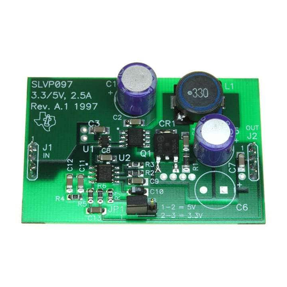
Input/Output Connections 1.3 Input/Output Connections Figure 1–3 shows the SLVP097 input and output connections. Figure 1–3. I/O Connections Power Supply – SLVP097 3.3/5 V, 2.5 AMP Rev. A.1 1997 .330 1–2 = 5 V 2–3 = 3.3 V – LOAD Notes: 1) The input power supply should be rated at least 3 A with current limit set high enough for proper operation. -
Page 11: 1.4 Board Layout
Board Layout 1.4 Board Layout Figures 1–4 through 1–6 show the SLVP097 board layout. Figure 1–4. Board Layout SLVP097 3.3/5V, 2.5 AMP Rev. A.1 1997 .330 1.6” 1–2 = 5V 2–3 = 3.3V 2.4” Figure 1–5. Top Layer 1.6” 2.4” Hardware... -
Page 12: Bottom Layer
Board Layout Figure 1–6. Bottom Layer 1.6” 2.4”... - Page 13 Bill of Material 1.5 Bill of Material Table 1–1 lists materials required for the SLVP097. Table 1–1. Bill of Materials Reference Part Number Description 20SA100M Sanyo Capacitor, Os-Con, 100 F, 20 V, F-case Capacitor, Ceramic, 0.1 F, 50 V, 1206 Capacitor, Ceramic, 0.1 F, 50 V, 1206 Capacitor, Ceramic, 1000 pF, 50 V, 1206...
-
Page 14: Output Voltage Vs Output Current (3.3-V Mode)
Test Results 1.6 Test Results Figures 1–7 through 1–11 show test results for the the SLVP097. Figure 1–7. Output Voltage Vs Output Current (3.3-V Mode) OUTPUT VOLTAGE OUTPUT CURRENT (3.3-V MODE) 3.45 V CC = 9 V 3.35 3.25 3.15 I O –... -
Page 15: Output Voltage Vs Supply Voltage (3.3-V Mode)
Test Results Figure 1–9. Output Voltage Vs Supply Voltage (3.3-V Mode) OUTPUT VOLTAGE SUPPLY VOLTAGE (3.3-V MODE) 3.26 3.255 I O = 0.25 A 3.25 3.245 I O = 2.5 A 3.24 3.235 3.23 V CC – Supply Voltage – V Figure 1–10. -
Page 16: Efficiency Vs Output Current (5-V Mode)
Test Results Figure 1–11. Efficiency Vs Output Current (5-V Mode) EFFICIENCY OUTPUT CURRENT 3.3 V V CC = 9 V I O – Output Current – A 1-10... - Page 17 Chapter 2 Design Procedure The SLVP097 evaluation module provides a method for evaluating the perfor- mance of the TPS2817 MOSFET driver and the TL5001 PWM controller. The TPS2817 contains all of the circuitry necessary to drive large MOSFETs, in- cluding a voltage regulator for higher voltage applications. This section ex- plains how to construct basic power conversion circuits including the design of the control chip functions and the basic loop.
- Page 18 Introduction 2.1 Introduction The SLVP097 is a dc-dc buck converter module that provides a 5-V or 3.3-V output at up to 2.5 A with an input voltage range of 5.5 V to 12 V. The controller is a TL5001 PWM operating at a nominal frequency of 275 kHz. The TL5001 is configured for a maximum duty cycle of 100 percent and has short-circuit protection built in.
- Page 19 Operating Specifications 2.2 Operating Specifications Table 2–1 lists the operating specifications for the SLVP097. Table 2–1. Operating Specifications Specification Units † Input Voltage Range 12.6 Output Voltage Range 5-V Mode 3.3-V Mode Output Current Range Operating Frequency Output Ripple Efficiency †...
-
Page 20: Duty Cycle Estimate
Detailed steps in the design of a buck-mode converter may be found in Designing With the TL5001C PWM Controller (literature number SLVA034) from Texas Instruments. This section shows the basic steps involved in this design, using the 3.3-V output mode. -
Page 21: Rectifier
Design Procedures Assuming total switching time, t , = 100 ns, a 55°C maximum ambient tem- perature, and r adjustment factor (for high temperature) = 1.6, then: DS(ON) 2.5 2 (0.04 1.6) 10 3 0.41 W The thermal impedance R = 90°C/W for FR-4 with 2-oz. -
Page 22: Loop Compensation
Design Procedures Soft-start is added to reduce power-up transients. This is implemented by adding a capacitor across the dead-time resistor. In this design, a soft-start time of 5 ms is used: 0.005 s 47 k The TL5001 has short circuit protection (SCP) instead of a current sense cir- cuit. -
Page 23: Power Stage Response
Design Procedures This information is enough to calculate the required compensation values. Figure 2–1 shows the power stage gain and phase plots. Figure 2–1. Power Stage Response FREQUENCY RESPONSE –45 –90 –135 –180 –225 –10 –270 –20 –315 –30 –360 10 2 10 3 10 4... - Page 24 Design Procedures The sum of the gains of the modulator, the LC filter, and the error amplifier needs to be 0 dB at the selected unity-gain frequency of 20 kHz. The modulator and LC filter gain is –14 dB. The two zeroes at 1.87 kHz in the compensation network that cancels the LC poles will have a total gain of 41.2 dB at 20 kHz.
- Page 25 Mouser Electronics Authorized Distributor Click to View Pricing, Inventory, Delivery & Lifecycle Information: Texas Instruments TL5001EVM-097 DC/DC-CONV...
Need help?
Do you have a question about the TL5001EVM-097 and is the answer not in the manual?
Questions and answers