Table of Contents
Advertisement
Quick Links
Advertisement
Table of Contents

Related Manuals for Kirisun FP520


Summary of Contents for Kirisun FP520
- Page 1 [键入文档副标题] [选取日期] [在此处键入文档的摘要。摘要通常是对文档内容的简短总结。在此处键入文档的摘要。摘要 通常是对文档内容的简短总结。]...
-
Page 2: Table Of Contents
FP520 Service Manual Contents Chapter 1 Overview ........................... 3 1. 1 Introduction ............................3 1.2 Safety Precautions ..........................3 Chapter 2 External View and Functional Keys ................... 4 2.1 External View ............................4 2.2 Functional Key Description ........................4 2.3 LED Indicator ............................5 Chapter 3 Circuit Description ........................ - Page 3 Figure 3 FP520-01Bottom Board Position Mark Diagram (136-174MHz) ..........52 Figure 4 FP520-02 Mainboard Schematic Diagram (400-470MHz) ............53 Figure 5 FP520-02 Top Board Position Mark Diagram (400-470MHz) ..........61 Figure 6 FP520-02 Bottom Board Position Mark Diagram(400-470MHz) ........... 62 Figure 7 KBC-51 7.4V Electrical Schematic Diagram ................
-
Page 4: Chapter 1 Overview
Chapter 1 Overview 1. 1 Introduction This manual applies to the service and maintenance of FP520 FM portable radios, and is intended for use by engineers and professional technicians that have been trained by Kirisun. It contains all the required service information for the equipment. -
Page 5: Chapter 2 External View And Functional Keys
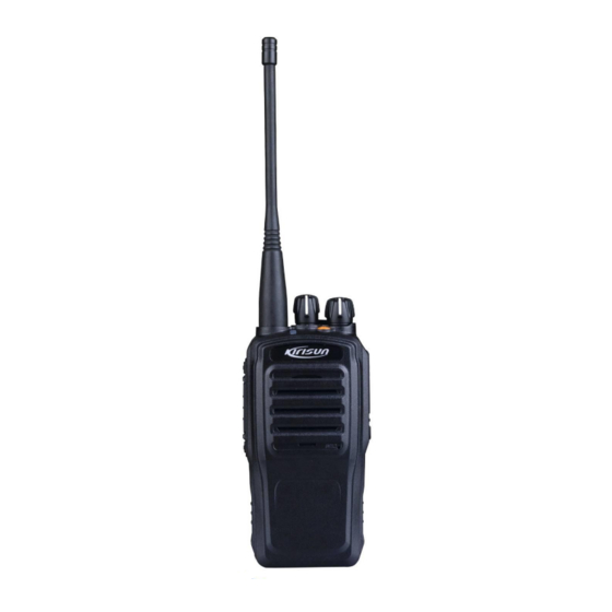
FP520 Service Manual Chapter 2 External View and Functional Keys 2.1 External View As figure 1 shows Fig. 1 2.2 Functional Key Description 1. Side Button 1(Programmable Button) 2. PTT(PUSH-TO-TALK)Button Press and hold the PTT button and talk to the microphone to transmit; release it to listen. -
Page 6: Led Indicator
FP520 Service Manual Programmable Button You can require the dealer to program the keys listed below as shortcuts to certain functions for your convenience: Long press key and short press key can be set: Side Button, Emergency Button. Long press key can be set: menu key, cancel key. -
Page 7: Chapter 3 Circuit Description
FP520 Service Manual Chapter 3 Circuit Description 3.1 Overview This radio is FM portable equipment. 3.2 Frequency Configuration 450KHz MIXER IF SYSTEM ANT SW 51.65MHz 12.8MHz TCXO multiply CODEC Fig 3.1 Circuit Diagram This Radio applies twice frequency mixing method. The first intermediate-frequency is 51.65MHz. The second intermediate-frequency is 450 kHz. -
Page 8: Principle Of Transmitter (Tx)
FP520 Service Manual Receiver Front End Signals from the antenna through the receiving/transmission (RX/TX) switch (D600,D601,D602,D603), which passed the band-pass filter (BPF) consisting of two levels of LC to eliminate the unnecessary signals, then sent to the low noise amplifier (LNA) consisting of Q703 and its peripheral components for enlargement. -
Page 9: Principle Of Frequency Synthesizer
FP520 Service Manual Fig.3.3 Diagram of Power Amplification and Antenna Switch Principle The modulated RF signal from VCO, being amplified by Q303、 Q304、 Q602、 Q603、 Q601, is sent to Q600 for power amplification. The grid bias of Q601 and Q600 is controlled by APC (Automatic Power Control) circuit. Change the grid bias voltage to easily control the output power strength of the transmitter. -
Page 10: Audio Processing Circuit
FP520 Service Manual comparison with reference frequency after being divided by the programmable frequency divider, and the error signal is then generated to change the oscillation frequency of VCO after filtered by the low pass filter. VCO is locked when the frequency of VCO reaches a certain set value. -
Page 11: Mcu Unit
FP520 Service Manual Q1:5C switch, controlled by MCU. 5C:The 5V power source controlled by power saving, and it supplies power for frequency synthesizer unit. 3.8 MCU Unit MCU unit controls every unit operation of the radio to perform all the radio functions. -
Page 12: Semiconductor Device Description
FP520 Service Manual 77.0 107.2 151.4 218.1 79.7 110.9 156.7 225.7 82.5 114.8 162.2 233.6 85.4 118.8 167.9 241.8 88.5 123.0 173.8 250.3 91.5 127.3 179.9 DCS Signaling: DCS(Digital code squelch,) ,a continuous numerical code which is modulated along with the speech signal on the carrier to control the squelch. - Page 13 FP520 Service Manual EPDT EEPROM data input/ output EPCK EEPROM clock BYTE CNVSS BSHIFT clock beat frequency control Min. volume control RESET CPU reset input XOUT CPU clock output CPU clock input PTT control pin input EXT-PTT External PTT control pin input...
- Page 14 FP520 Service Manual RED_LED red light control switch 5T control pin 5R control pin SAVE 5C control pin INTO data output pin(connects 3252) PLLBYPASS data output pin(connects 3252) PLLSEL2 data output pin(connects 3252) HCSN data output pin(connects 3252) HWRN data input pin(connects 3252)...
- Page 15 FP520 Service Manual VOL_DET digital potentiometer detection pin extension key detection pin HEADPHONE_DET VREF AVCC GPS_C GPS power control pin BASSBAND_C power time-delay control pin BEEP_C BEEP control pin Chart 3.4 Semiconductor Device Function Description Position No. Item No. Function Description...
- Page 16 FP520 Service Manual Q602 2SC5108 transmitter 1 amplification Q603 2SC3356 transmitter 2rd amplification Q604 DTA144EE APC output switch Q703 3SK318 receiver low noise amplifier Q702 3SK318 the 1 level frequency mixer Q701 2SC5108 the 1 intermediate frequency amplifier Q700 2SC4617...
-
Page 17: Chapter 4 Function Description And Parameter Settings
FP520 Service Manual Chapter 4 Function Description and Parameter Settings 4.1 Time-out Timer This feature prevents the user from long occupation of the channel. If the transmitting period exceeds the dealer’s preprogrammed time, the radio stops transmitting and the rings alert tone. To stop the alert tone, please release the PTT button. -
Page 18: Parameter Settings
D.Turn on the Radio. E.Click the execution procedure, and operate FP520 programming software. F.In the main menu of FP520 programming software, click “read” menu to input the radio parameter into the computer. G.For detailed operation, please refer to the “assistance” file of the programming software. -
Page 19: Chapter 5 Assembly And Disassembly
FP520 Service Manual Chapter 5 Assembly and Disassembly This radio is sophiscated communication equipment with a precise and compact mechanism. The assembly and disassembly of the radio must be carefully done during the repair. The description is as follows: 5.1 Installing/Removing the Battery Installing the Battery: Press ①... -
Page 20: Installing/Removing The Antenna (See Fig. 20)
FP520 Service Manual 5.2 Installing/Removing the Antenna (see Fig. 20) When installing, put the antenna end with screw thread into the threaded hole of the radio top, and turn it clockwise until it is fastened. For the removing, hold the antenna bottom and turn it counterclockwise. -
Page 21: Separating The Front Cover From The Chassis (See Fig. 23)
FP520 Service Manual 5.5 Separating the Front Cover from the Chassis (see Fig. 23) 1. Removing the antenna, volume knob and channel knob; 2. Removing the two knob nuts and one antenna nut; 3. Removing the two aluminum screws with wabblers;... - Page 22 FP520 Service Manual Part no. Description Quantity Remark 7SMF-020040M-SZYB-N M2*4 round flat head fixes the PCB board, PTT button and machine screw antenna screw 7MHP-4083-01A-W0 FP520 front cover ABS+PC;black;silk screen/texturing Φ6.0, -40± 2dB omnidirectional,2.2KΩ,2V, 4SM7-6027-A40C MIC microphone with 80mm red black wire...
- Page 23 FP520 Service Manual 7MHR-7208-04A-W9 light pipe silica gel; transparent ; milk white 7MHR-7208-06A-W0 silica gel side button silica gel; black 7MHP-7208-05A-W0 PTT cover ABS+PC,black; texturing 7MHS-1140-01A-W knob circlip Material: spring steel 7MHP-7208-01A-W0 volume knob ABS;black; white paint 7MHP-7208-02A-W0 channel knob ABS;black;...
-
Page 24: Chapter 6 Adjustment
FP520 Service Manual φ6mm,SUS301 square metal dome 7MHS-4083-01A-W PTT button metal dome 6PD7-4083-HPA PTT PCB 6PM7-4085-HMB(VHF) main PCB 1.2mm thickness 6PM7-4083-HMB(UHF) 7MHS-7042-01B-W latch spring2 stainless steel (SUS301),0.25THK 7MHS-7042-01A-W latch spring1 stainless steel(SUS301),0.25THK 7MHP-7042-14A-W0 battery latch POM,black 7MHX-7042-02B-Z battery hook 2... -
Page 25: Radio Test
FP520 Service Manual adjusted to 0.8-1.1W. 3). The Maximum Frequency Deviation (the modulation signal is 1kHz/120mV) Under the computer mode [the maximum audio frequency deviation] (the broadband has five frequencies and the narrowband has one; six frequencies in total), adjust the maximum transmitting frequency deviation to 1.8-2.5 kHz. -
Page 26: Chapter 7 Major Specifications
FP520 Service Manual Receiving working current: <=400mA 4). QT/DQT decode: <= -116dBm (0.35uV) (broad band, narrow band) the radio could decode correctly. 5).Sensitivity of squelch-off:the RF input ≤ -124dBm,the squelch feature should be disabled. 6). Sensitivity of squelch-on: the RF input ≥- 119dBm,the squelch feature should be enabled. -
Page 27: Rx Part
FP520 Service Manual 7.2 RX Part ≤0.25μV Sensitivity (12dB SINAD) ≤0.18uV Squelch-On Sensitivity ≤-35dB Receiver Residual Output Modulation Receiving Bandwidth ± 3.5kHz ≥50dB Adjacent Channel Selectivity ≥65dB Intermodulation Interference Rejection ≥70dB Spurious Response Rejection Audio Output Power 1.3W,BTL @Distortion≤10%,16Ω ≤400mA Receiving Consumption Current 7.3 TX Part... -
Page 28: Chapter 8 Service And Test Equipment
FP520 Service Manual Chapter 8 Service and Test Equipment During the service and test, the following equipment and apparatus are needed. Equipment Specification Standard Signal Frequency Range: 136-174MHz, 400-470MHz Generator Modulation: FM and External Modulation -127dBm/0.1uv or ≥-47dBm/1mv Output: 50Ω... -
Page 29: Chapter 9 Kbc-51 Charger
FP520 Service Manual Chapter 9 KBC-51 Charger 9.1 The Operational Conditions and Basic Specification of Charger a) Battery Specification:Li-ion(2*3.7V) ,Ni-MH (6*1.2V),battery capacity (1~2.4AH). b)Power Adaptor Specification: DC 11V~16V,500~1500mA power adaptor,standard voltage is 12V. c) No-load Input Current:≤ 15mA d) Precharged Current:75 mA± 10 mA e) Precharged Time Limit:15Min... -
Page 30: Chapter 10 Troubleshooting
FP520 Service Manual Chapter 10 Troubleshooting Problems Causes and Solutions Power-on Failure A.The battery pack may be out of power. Please charge it or change to a new one, then try again. B.The power switch failure. Change to a new power switch. -
Page 31: Appendix 1 Abbreviation
FP520 Service Manual Appendix 1 Abbreviation Amplify, Amplifier Antenna Automatic Power Control Band Pass Filter CTCSS Continuous Tone Control Squelch System Digital Code Squelch DEMOD Demodulation PROM Electrically Erasable Programmable Read-Only Memory High Pass Filter) Instantaneous Deviation Control Intermediate Frequency... -
Page 32: Appendix 2 Spare Part List (Electronic Part 400-470Mhz)
FP520 Service Manual Appendix 2 Spare Part List (Electronic Part 400-470MHz) Part No. Item Name. Specification Quantit Plug-in Position 6PM7-4083-HMB FP520 PCB Board FP520U-MAIN-140106.PCB;1.0MM;47X101.5MM;FR-4, four layers, Mainboard PCB Pb-free 1DS1-HSC277 Chip switch diode HSC277,1608 D402, D602, D700 1DS1-HVC131 Chip switch diode... - Page 33 FP520 Service Manual 2CC1-10-C0G500-120J Chip multilayer capacitance 1005,12P±5%,50V,C0G C331, C363 2CC1-10-C0G500-150J Chip multilayer capacitance 1005,15P±5%,50V,C0G C327 2CC1-10-C0G500-160J Chip multilayer capacitance 1005,16P±5%,50V,C0G C311 2CC1-10-C0G500-180J Chip multilayer capacitance 1005,18P±5%,50V,C0G C620, C732 2CC1-10-C0G500-220J Chip multilayer capacitance 1005,22P±5%,50V,C0G C225, C227, C618 2CC1-10-C0G500-270J Chip multilayer capacitance 1005,27P±...
- Page 34 FP520 Service Manual 2CC1-16-C0G500-6R0C Chip multilayer capacitance 1608,6P± 0.25P ,50V,C0G C608 2CC1-16-C0G500-6R0D Chip multilayer capacitance 1608,6P± 0.5P,50V,C0G C609 2CC1-16-X7R500-471K Chip multilayer capacitance 1608,470P±10%,50V,X7R C611 2CC1-20-Y5V160-106Z chip multilayer capacitance 2012,10uF+80%/-20%,16V,Y5V C8, C9, C11, C15, C16, C17, C18, C63, C103, C106, C109, C116, C119, C319, C344, C348, C642, C750, C752, C802, C806, C815, C817, C49 3216,1μF±20%,16V,TS series (A level)
- Page 35 FP520 Service Manual 2RS1-10-103J chip resistance 1005,10K±5% R809, R815, R822, R806, R32,R227, R8, R33, R34, R35, R36, R37, R43, R100, R103, R250, R251, R252, R327, R337, R338, R339, R340, R344, R718, R801, R816, 2RS1-10-104J chip resistance 1005,100K±5% R105, R342, R704, R724, R727, R739, R316, R4, C7...
- Page 36 FP520 Service Manual 2RS1-16-153J Chip resistance 1608,15K±5% R615 2012,0Ω 2RS1-20-000O Chip resistance L707 3216,0.47Ω±5% 2RS1-32-R47J Chip resistance R620, R621, R622 2RT1-NTH5G16P42B104K chip thermal resistance 1608,NTH5G16P42B104K07TH R707 3ST1-SKRTLBE010 chip touch switch SKRTLBE010,4.5*3.55*3.3mm(ALPS) 4PE1-16-F2 chip LED 1608, red light, 19-21SUR/S530-A2/TR8 D202 4PE1-16-F5...
-
Page 37: Appendix 3 Spare Part List (Electronic Part 136-174Mhz)
FP520 Service Manual Appendix 3 Spare Part List (Electronic Part 136-174MHz) Part No. Name Specification Quantity Plug-in Position 6PM7-4085-HMB FP520 VHF main board FP520V-MAIN-140106.PCB;1.0MM;47X101.5MM;FR-4;four layers; FP520- VHF mainboard PCB Pb-free 7MHP-7042-12A-W battery connector (subassembly) 1DS1-DA2S10100L Chip switch diode DA2S10100L D309, D310, D709... - Page 38 FP520 Service Manual 1TT1-FMMT717TA Chip triode FMMT717A,PNP,SOT23 Q800 1TT1-KTA1298-Y Chip triode KTA1298-Y,SOT23 Q1, Q3, Q100, Q102 2CA1-TZVY2Z100A110 chip trimmer capacitance 2-10P,+100/-0%,NP0±300PPm/℃ C335, C371 2CC1-10-C0G500-100D Chip multilayer capacitance 1005,10P±0.5P,50V,C0G C308, C309, C318, C321, C328 2CC1-10-C0G500-101J Chip multilayer capacitance 1005,100P±5%,50V,C0G C612, C765, C375, C643, C725, C751...
- Page 39 FP520 Service Manual 2CC1-16-C0G500-180J Chip multilayer capacitance 1608,18P±5%,50V,C0G C515 2CC1-16-C0G500-270J Chip multilayer capacitance 1608,27P±5%,50V,C0G 2CC1-16-C0G500-330J Chip multilayer capacitance 1608,33P±5%,50V,C0G C326 2CC1-16-C0G500-5R0C Chip multilayer capacitance 1608,5P± 0.25P,50V,C0G C365 2CC1-16-C0G500-680J Chip multilayer capacitance 1608,68P±5%,50V,C0G C66, C634 2CC1-16-C0G500-7R0D Chip multilayer capacitance 1608,7P± 0.5P,50V,C0G...
- Page 40 FP520 Service Manual 2LW1-25UC-821K chip wire wound inductance 2520,820nH± 10%, ceramic core (FLM2520-R82K) L705 2RE1-16-1503 chip precision resistance 1608,150K±1% R617 R618 R619 R624 R625 R627 R628 1005,0Ω 2RS1-10-000O chip resistance C700,C2,C3,C73,C74,R65,C226 R1, R16, R17, R18, R39, R40, R107, R143, R604, R616, R20, R824, R721, R739, C721, R206, R13, R14, R19, R60, R41 1005,10Ω±5%...
- Page 41 LED 1608,red light,19-21SUR/S530-A2/TR8 D202 4PE1-16-F5 chip LED 1608,green light ,H19-213SYGC D203 5FC1-D51606GQ1-0705 chip crystal filter FP520 DSF753SDF,51.65MHz± 3KHz/5dB,7.0*5.0*1.3 5FE1-BLM11A221SPT chip EMI suppression filter 1608,BLM11A221SPT/BLM18AG221S(0138-05) FB1, FB7, FB8, FB9, FB12, FB16, FB17, L4, L5 5FE1-BLM11A601S chip EMI suppression filter 1608,BLM11A601S/BLM18AG601S(0138-05)
-
Page 42: Appendix 4 Spare Part List (Structural Material)
FP520 Service Manual Appendix 4 Spare Part List (Structural Material) Part No. Part Name Specification Quantity 7MHP-7208-01B-W0 volume knob Material: ABS,black,white; shares the same front mould with PT7200;140307 revised, Pb-free 7MHP-7208-02A-W0 channel knob Material: ABS, black, white; shares the same front mould with PT7200; Pb-free... -
Page 43: Appendix 5 Accessory List
FP520 Service Manual 7MHZ-1731-01A-J5 speaker insulation paper Material: dark green highland barley paper, length 18mm*width 8mmthickness 0.2mm,rubber on single side 7MHS-4083-01A-W PTT button metal dome Material:φ6mm,SUS301 square metal dome; Lixinghui; Pb-free Appendix 5 Accessory List Accessory Quantity Antenna Battery Belt Clip... -
Page 44: Figure 1 Fp520-01 Mainboard Schematic Diagram (136-174Mhz)
FP520 Service Manual Figure 1 FP520-01 Mainboard Schematic Diagram (136-174MHz) Page 43 of 64... - Page 45 FP520 Service Manual Page 44 of 64...
- Page 46 FP520 Service Manual Page 45 of 64...
- Page 47 FP520 Service Manual Page 46 of 64...
- Page 48 FP520 Service Manual Page 47 of 64...
- Page 49 FP520 Service Manual Page 48 of 64...
- Page 50 FP520 Service Manual Page 49 of 64...
- Page 51 FP520 Service Manual Page 50 of 64...
-
Page 52: Figure 2 Fp520-01Top Board Position Mark Diagram (136-174Mhz)
FP520 Service Manual Figure 2 FP520-01Top Board Position Mark Diagram (136-174MHz) Page 51 of 64... -
Page 53: Figure 3 Fp520-01Bottom Board Position Mark Diagram (136-174Mhz)
FP520 Service Manual Figure 3 FP520-01Bottom Board Position Mark Diagram (136-174MHz) Page 52 of 64... -
Page 54: Figure 4 Fp520-02 Mainboard Schematic Diagram (400-470Mhz)
FP520 Service Manual Figure 4 FP520-02 Mainboard Schematic Diagram (400-470MHz) Page 53 of 64... - Page 55 FP520 Service Manual Page 54 of 64...
- Page 56 FP520 Service Manual Page 55 of 64...
- Page 57 FP520 Service Manual Page 56 of 64...
- Page 58 FP520 Service Manual Page 57 of 64...
- Page 59 FP520 Service Manual Page 58 of 64...
- Page 60 FP520 Service Manual Page 59 of 64...
- Page 61 FP520 Service Manual Page 60 of 64...
-
Page 62: Figure 5 Fp520-02 Top Board Position Mark Diagram (400-470Mhz
FP520 Service Manual Figure 5 FP520-02 Top Board Position Mark Diagram (400-470MHz) Page 61 of 64... -
Page 63: Figure 6 Fp520-02 Bottom Board Position Mark Diagram(400-470Mhz
FP520 Service Manual Figure 6 FP520-02 Bottom Board Position Mark Diagram(400-470MHz) Page 62 of 64... -
Page 64: Figure 7 Kbc-51 7.4V Electrical Schematic Diagram
FP520 Service Manual Figure 7 KBC-51 7.4V Electrical Schematic Diagram Page 63 of 64...
Need help?
Do you have a question about the FP520 and is the answer not in the manual?
Questions and answers