
Related Manuals for Aaeon GES-3300F


Summary of Contents for Aaeon GES-3300F
- Page 1 G r e e n E m b e d d e d S y s t e m G E S - 3 3 0 0 F GES-3300F Green Embedded System 2.5” SATA Hard Disk Drive Bay 2 Gigabit Ethernet Ports/ 4 COM / 6 USB2.0 CompactFlash™ GES-3300F Manual 2nd Ed. October 2010...
-
Page 2: Copyright Notice
AAEON assumes no liabilities resulting from errors or omissions in this document, or from the use of the information contained herein. AAEON reserves the right to make changes in the product design without notice to its users. - Page 3 G r e e n E m b e d d e d S y s t e m G E S - 3 3 0 0 F Acknowledgments All other products’ name or trademarks are properties of their respective owners. •...
-
Page 4: Packing List
Packing List Before you begin operating your PC, please make sure that the following materials are enclosed: GES-3300F Bare Bone CD-ROM for manual (in PDF format) and drivers 130W AC-DC Power Adapter If any of these items should be missing or damaged, please contact... - Page 5 G r e e n E m b e d d e d S y s t e m G E S - 3 3 0 0 F Safety & Warranty 1. Read these safety instructions carefully. 2. Keep this user's manual for later reference. 3.
- Page 6 G r e e n E m b e d d e d S y s t e m G E S - 3 3 0 0 F The equipment does not work well, or you cannot get it to work according to the user’s manual. The equipment has been dropped and damaged.
- Page 7 G r e e n E m b e d d e d S y s t e m G E S - 3 3 0 0 F Below Table for China RoHS Requirements 产品中有毒有害物质或元素名称及含量 AAEON Boxer/ Industrial System 有毒有害物质或元素 部件名称 铅...
- Page 8 G r e e n E m b e d d e d S y s t e m G E S - 3 3 0 0 F Contents Chapter 1 General Information 1.1 Introduction..............1-2 1.2 Features ..............1-3 1.3 Specifications ............
- Page 9 G r e e n E m b e d d e d S y s t e m G E S - 3 3 0 0 F 2.16 Internal Keyboard Connector (CN9) ...... 2-10 2.17 Internal Mouse Connector (CN10) ......2-11 2.18 LVDS-LCD Connector (CN11) ......
- Page 10 G r e e n E m b e d d e d S y s t e m G E S - 3 3 0 0 F 3.2 Award BIOS Setup ............ 3-3 Chapter 4 Driver Installation 4.1 Installation ..............4-3 Appendix A Programming The Watchdog Timer A.1 Programming ............A-2 A.2 IT8712 Watchdog Timer Initial Program ....A-6...
- Page 11 G r e e n E m b e d d e d S y s t e m G E S - 3 3 0 0 F Chapter General Information 1- 1 Chapter 1 General Information...
-
Page 12: Introduction
This compact GES-3300F equipped with one internal 2.5” Hard Disk Drive with SATA II interface. In addition, it features four COM ports and six USB2.0. Furthermore, the GES-3300F deploys AC97 Audio Stereo Amplifier to support the audio function. -
Page 13: Features
G r e e n E m b e d d e d S y s t e m G E S - 3 3 0 0 F 1.2 Features Compact Size & Fanless ® ® Intel Core™ 2 Duo/ Core™ Duo/ Celeron M Processor, Fanless Design CPU TDP <... -
Page 14: Specifications
G r e e n E m b e d d e d S y s t e m G E S - 3 3 0 0 F 1.3 Specifications System Form Factor Compact size for Desktop/Wallmount ® Processor Intel Core™... - Page 15 G r e e n E m b e d d e d S y s t e m G E S - 3 3 0 0 F External I/O RS-232 x 3, RS-232/422/485 x 1 Serial Port KB & Mouse Keyboard /Mouse x 1 Universal Serial Bus USB2.0 x 6 (4 on the front panel and 2 on the rear panel)
-
Page 16: General System Information
G r e e n E m b e d d e d S y s t e m G E S - 3 3 0 0 F 1.4 General System Information Front Panel 1- 6 Chapter 1 General Information... -
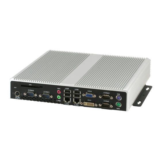
Page 17: Rear Panel
G r e e n E m b e d d e d S y s t e m G E S - 3 3 0 0 F Rear Panel 1- 7 Chapter 1 General Information... -
Page 18: Installation
G r e e n E m b e d d e d S y s t e m G E S - 3 3 0 0 F Chapter Hardware Installation Chapter 2 Hardware Installation... -
Page 19: Location Of Jumpers And Connector
G r e e n E m b e d d e d S y s t e m G E S - 3 3 0 0 F 2.1 Location of Jumpers and Connectors Main board Chapter 2 Hardware Installation... -
Page 20: Mechanical Drawing
G r e e n E m b e d d e d S y s t e m G E S - 3 3 0 0 F 2.2 Mechanical Drawing DIO Pin Definition Chapter 2 Hardware Installation... -
Page 21: List Of Jumpers
G r e e n E m b e d d e d S y s t e m G E S - 3 3 0 0 F 2.3 List of Jumpers The board has a number of jumpers that allow you to configure your system to suit your application. -
Page 22: List Of Connectors
G r e e n E m b e d d e d S y s t e m G E S - 3 3 0 0 F 2.4 List of Connectors The board has a number of connectors that allow you to configure your system to suit your application. - Page 23 G r e e n E m b e d d e d S y s t e m G E S - 3 3 0 0 F CN21 USB Connector CN22 Digital I/O Connector CN23 COM4 RS-232 Serial Port Connector CN24 COM3 RS-232 Serial Port Connector CN25...
-
Page 24: Setting Jumpers
G r e e n E m b e d d e d S y s t e m G E S - 3 3 0 0 F 2.5 Setting Jumpers You configure your card to match the needs of your application by setting jumpers. -
Page 25: Com2 Ring/ +5V/ +12V Selection (Jp2)
G r e e n E m b e d d e d S y s t e m G E S - 3 3 0 0 F 2.6 COM2 Ring/+5V/+12V Selection (JP2) Function +12V Ring (Default) 2.7 LCD INVERTER Voltage Selection (JP3) Function +5V(Default) +12V... -
Page 26: Com2 Rs-232/422/485 Connector (Cn2)
G r e e n E m b e d d e d S y s t e m G E S - 3 3 0 0 F 2.11 COM2 RS-232/422/485 Connector (CN2) Signal Signal DCD (422TXD-/485DATA-) RXD (422RXD+) TXD (422TXD+/485DATA+) DTR (422RXD-) N.C. -
Page 27: Tv-Out Connector (Cn6)
G r e e n E m b e d d e d S y s t e m G E S - 3 3 0 0 F 2.13 TV-out Connector (CN6) Signal Signal CVBS N.C. N.C. 2.14 LCD Inverter Connector (CN7) Signal VCC of LCD inverter (+5V/+12V) Adjust backlight... -
Page 28: Internal Mouse Connector (Cn10)
G r e e n E m b e d d e d S y s t e m G E S - 3 3 0 0 F 2.17 Internal Mouse Connector (CN10) Signal MS_CLK MS_DATA 2.18 LVDS-LCD Connector (CN11) Signal Signal ENBKL... -
Page 29: Sdvo Connector (Cn12)
G r e e n E m b e d d e d S y s t e m G E S - 3 3 0 0 F LVDS2_TXCLK- LVDS2_TXCLK+ 2.19 SDVO Connector (CN12) Signal Signal SDVO_SPC SDVO_RST# SDVO_SPD SMBCLK N.C. -
Page 30: System Fan Connector (Cn13)
G r e e n E m b e d d e d S y s t e m G E S - 3 3 0 0 F 2.20 System Fan Connector (CN13) Signal VCC of FAN Speed Sense Speed Control 2.21 RTC Battery Connector (CN14) Signal Battery Power input... -
Page 31: Atx Power Connector (Cn16)
G r e e n E m b e d d e d S y s t e m G E S - 3 3 0 0 F 2.23 ATX Power Connector (CN16) Signal Signal N.C. N.C. N.C. -12V PS_ON POWER OK +5VSB +12V... -
Page 32: At Power Connector (Cn18)
G r e e n E m b e d d e d S y s t e m G E S - 3 3 0 0 F BUSY SELECT N.C. 2.25 AT Power Connector (CN18) Signal N.C. +12V -12V 2.26 PCI-Express Slot (CN19) Signal Signal... - Page 33 G r e e n E m b e d d e d S y s t e m G E S - 3 3 0 0 F N.C. N.C. +3.3V +3.3V N.C. +3.3V +3.3VSB PCIE_RESET# PCIE_WAKE# N.C. PCIE1_CLKP PCIE1_CLKN PCIE1_TXP PCIE1_TXN PCIE1_RXP...
-
Page 34: Usb Connector (Cn20 & Cn21)
G r e e n E m b e d d e d S y s t e m G E S - 3 3 0 0 F PCIE2_CLKP 2.27 USB Connector (CN20 & CN21) Signal Signal USBD1- USBD1+ USBD2+ USBD2- 2.28 Digital I/O Connector (CN22) This connector offers 4-pair of digital I/O functions and address is 2A1H. -
Page 35: Com4 Rs-232 Serial Port Connector (Cn23)
G r e e n E m b e d d e d S y s t e m G E S - 3 3 0 0 F 8 in Pin1 Pin2 Pin3 Pin4 Pin5 Pin6 Pin7 Pin8 GPI 27 GPI 26 GPI 25 GPI 24... -
Page 36: Com6 Rs-232 Serial Port Connector (Cn25)
G r e e n E m b e d d e d S y s t e m G E S - 3 3 0 0 F 2.31 COM6 RS-232 Serial Port Connector (CN25) Signal Signal N.C. 2.32 IrDA Connector (CN26) Signal N.C. -
Page 37: Audio Speaker Output (Cn30)
Reset Switch (-) Reset Switch (+) 2.35 Audio Speaker Output (CN30) Signal SPK-R+ SPK-R- SPK-L+ SPK-L- 2.36 Installing the Hard Disk Drive Step 1: Unfasten the five screws on the bottom case of the GES-3300F 2-20 Chapter 2 Hardware Installation... - Page 38 G E S - 3 3 0 0 F Step 2: Take the three screws out of the case, and take the HDD case out of the GES-3300F Step 3: Disconnect the SATA and Power cables (The CompactFlash card is optional.
- Page 39 G r e e n E m b e d d e d S y s t e m G E S - 3 3 0 0 F Step 4: Unfasten the four screws to release the CompactFlash Card Step 5: Get the HDD case from the GES-3300F 2-22 Chapter 2 Hardware Installation...
- Page 40 G r e e n E m b e d d e d S y s t e m G E S - 3 3 0 0 F Step 6: Get the HDD ready and fasten the four screws covered by damper on HDD and put the HDD back to the case Note: Please be careful of the direction of the HDD when you put the HDD back to the case...
- Page 41 G r e e n E m b e d d e d S y s t e m G E S - 3 3 0 0 F Step 7: Plug the SATA cable and power cable Step 8: Place the HDD case to the GES-3300F and press the case to insert the HDD to the GES-3300F 2-24...
- Page 42 G r e e n E m b e d d e d S y s t e m G E S - 3 3 0 0 F Step 9: Done installing the HDD. Close and screw the bottom case of the GES-3300F 2-25 Chapter 2 Hardware Installation...
-
Page 43: Bios Setup
G r e e n E m b e d d e d S y s t e m G E S - 3 3 0 0 F Chapter Award BIOS Setup Chapter 3 Award BIOS Setup 3-1... -
Page 44: System Test And Initialization
3. The CMOS memory has lost power and the configuration information has been erased. The GES-3300F CMOS memory has an integral lithium battery backup for data retention. However, you will need to replace the complete unit when it finally runs down. -
Page 45: Award Bios Setup
G r e e n E m b e d d e d S y s t e m G E S - 3 3 0 0 F 3.2 Award BIOS Setup Awards BIOS ROM has a built-in Setup program that allows users to modify the basic system configuration. - Page 46 Save CMOS value changes to CMOS and exit setup. Exit Without Saving Abandon all CMOS value changes and exit setup. You can refer to the "AAEON BIOS Item Description.pdf" file in the CD for the meaning of each setting in this chapter. Chapter 3 Award BIOS Setup 3-4...
- Page 47 G r e e n E m b e d d e d S y s t e m G E S - 3 3 0 0 F Chapter Driver Installation Chapter 4 Driver Installation...
- Page 48 G r e e n E m b e d d e d S y s t e m G E S - 3 3 0 0 F The GSE-3300F comes with an AutoRun CD-ROM that contains all drivers and utilities that can help you to install the driver automatically.
- Page 49 G r e e n E m b e d d e d S y s t e m G E S - 3 3 0 0 F 4.1 Installation: Insert the GES-3300F CD-ROM into the CD-ROM drive and install the drivers from Step 1 to Step 4 in order. Step 1 – Install Chip Driver Click on the Step 1-chip folder and double click on the Setup.exe...
- Page 50 G r e e n E m b e d d e d S y s t e m G E S - 3 3 0 0 F your system is Double click on .exe located in each OS folder Follow the instructions that the window shows The system will help you install the driver automatically Chapter 4 Driver Installation...
-
Page 51: Watchdog Timer
G r e e n E m b e d d e d S y s t e m G E S - 3 3 0 0 F Appendix Programming the Watchdog Timer Appendix A Programming the Watchdog Timer A-1... -
Page 52: A.1 Programming
G r e e n E m b e d d e d S y s t e m G E S - 3 3 0 0 F A.1 Programming GES-3300F utilizes ITE 8712 chipset as its watchdog timer controller. Below are the procedures to complete its configuration and the AAEON intial watchdog timer program is also attached based on which you can develop customized program to fit your application. - Page 53 G r e e n E m b e d d e d S y s t e m G E S - 3 3 0 0 F There are three steps to complete the configuration setup: (1) Enter the MB PnP Mode; (2) Modify the data of configuration registers; (3) Exit the MB PnP Mode.
- Page 54 G r e e n E m b e d d e d S y s t e m G E S - 3 3 0 0 F WatchDog Timer Configuration Registers Configure Control (Index=02h) This register is write only. Its values are not sticky; that is to say, a hardware reset will automatically clear the bits, and does not require the software to clear them.
- Page 55 G r e e n E m b e d d e d S y s t e m G E S - 3 3 0 0 F WatchDog Timer Configuration Register (Index=72h, Default=00h) WatchDog Timer Time-out Value Register (Index=73h, Default=00h) Appendix A Programming the Watchdog Timer A-5...
-
Page 56: A.2 It8712 Watchdog Timer Initial Program
G r e e n E m b e d d e d S y s t e m G E S - 3 3 0 0 F A.2 IT8712 Watchdog Timer Initial Program .MODEL SMALL .CODE Main: CALL Enter_Configuration_mode CALL Check_Chip mov cl, 7 call Set_Logic_Device... - Page 57 G r e e n E m b e d d e d S y s t e m G E S - 3 3 0 0 F ; game port enable mov cl, 9 call Set_Logic_Device Initial_OK: CALL Exit_Configuration_mode MOV AH,4Ch INT 21h Enter_Configuration_Mode PROC NEAR...
- Page 58 G r e e n E m b e d d e d S y s t e m G E S - 3 3 0 0 F Exit_Configuration_Mode ENDP Check_Chip PROC NEAR MOV AL,20h CALL Read_Configuration_Data CMP AL,87h JNE Not_Initial MOV AL,21h CALL Read_Configuration_Data CMP AL,12h...
- Page 59 G r e e n E m b e d d e d S y s t e m G E S - 3 3 0 0 F MOV DX,WORD PTR CS:[Cfg_Port+06h] IN AL,DX Read_Configuration_Data ENDP Write_Configuration_Data PROC NEAR MOV DX,WORD PTR CS:[Cfg_Port+04h] OUT DX,AL XCHG AL,AH MOV DX,WORD PTR CS:[Cfg_Port+06h]...
- Page 60 G r e e n E m b e d d e d S y s t e m G E S - 3 3 0 0 F push ax push cx xchg al,cl mov cl,07h call Superio_Set_Reg pop cx pop ax Set_Logic_Device endp ;Select 02Eh->Index Port, 02Fh->Data Port...
- Page 61 G r e e n E m b e d d e d S y s t e m G E S - 3 3 0 0 F Appendix I/O Information Appendix B I/O Information...
-
Page 62: B.1 I/O Address Map
G r e e n E m b e d d e d S y s t e m G E S - 3 3 0 0 F B.1 I/O Address Map Appendix B I/O Information... -
Page 63: B.2 Memory Address Map
G r e e n E m b e d d e d S y s t e m G E S - 3 3 0 0 F B.2 Memory Address Map Appendix B I/O Information... -
Page 64: B.3 Irq Mapping Chart
G r e e n E m b e d d e d S y s t e m G E S - 3 3 0 0 F B.3 IRQ Mapping Chart B.4 DMA Channel Assignments Appendix B I/O Information...
Need help?
Do you have a question about the GES-3300F and is the answer not in the manual?
Questions and answers