Table of Contents
Advertisement
Quick Links
Advertisement
Table of Contents

Related Manuals for Clevo W540EU


Summary of Contents for Clevo W540EU
- Page 1 W540EU...
- Page 3 Preface Notebook Computer W540EU Service Manual...
- Page 4 Preface Notice The company reserves the right to revise this publication or to change its contents without notice. Information contained herein is for reference only and does not constitute a commitment on the part of the manufacturer or any subsequent ven- dor.
- Page 5 This manual is intended for service personnel who have completed sufficient training to undertake the maintenance and inspection of personal computers. It is organized to allow you to look up basic information for servicing and/or upgrading components of the W540EU series notebook PC.
- Page 6 Preface IMPORTANT SAFETY INSTRUCTIONS Follow basic safety precautions, including those listed below, to reduce the risk of fire, electric shock and injury to per- sons when using any electrical equipment: 1. Do not use this product near water, for example near a bath tub, wash bowl, kitchen sink or laundry tub, in a wet basement or near a swimming pool.
-
Page 7: Instructions For Care And Operation
Preface Instructions for Care and Operation The notebook computer is quite rugged, but it can be damaged. To prevent this, follow these suggestions: Don’t drop it, or expose it to shock. If the computer falls, the case and the components could be damaged. Do not expose the computer Do not place it on an unstable Do not place anything heavy... -
Page 8: Power Safety
Preface Avoid interference. Keep the computer away from high capacity transformers, electric motors, and other strong mag- netic fields. These can hinder proper performance and damage your data. Take care when using peripheral devices. Use only approved brands of Unplug the power cord before peripherals. -
Page 9: Battery Precautions
Preface Battery Precautions • Only use batteries designed for this computer. The wrong battery type may explode, leak or damage the computer. • Do not continue to use a battery that has been dropped, or that appears damaged (e.g. bent or twisted) in any way. Even if the computer continues to work with a damaged battery in place, it may cause circuit damage, which may possibly result in fire. -
Page 10: System Startup
Preface Related Documents You may also need to consult the following manual for additional information: User’s Manual on CD/DVD This describes the notebook PC’s features and the procedures for operating the computer and its ROM-based setup pro- gram. It also describes the installation and operation of the utility programs provided with the notebook PC. System Startup 1. -
Page 11: Table Of Contents
Preface Contents Introduction ..........1-1 SATA BLU RAY COMBO ............A-5 DVD DUAL ................... A-6 Overview ..................1-1 Dummy ODD ................. A-7 Specifications ..................1-2 LCD ....................A-8 External Locator - Top View with LCD Panel Open ......1-4 Schematic Diagrams......... B-1 External Locator - Front & Right Side Views .........1-5 External Locator - Left Side &... - Page 12 Preface HDMI, RJ45 ................. B-27 AUDIO CODEC VT1802P ............B-28 KBC-ITE IT8518E ............... B-29 5VS, 3VS, 1.5VS CPU ..............B-30 VDD3, VDD5 ................B-31 Power 0.85VS, 1.8VS ..............B-32 POWER 1.5V/1.05VS ..............B-33 POWER VCORE1 ............... B-34 POWER VCORE2 ............... B-35 AC IN, CHARGER ..............
-
Page 13: Introduction
Chapter 1: Introduction Overview This manual covers the information you need to service or upgrade the W540EU series notebook computer. Information about operating the computer (e.g. getting started, and the Setup utility) is in the User’s Manual. Information about dri- vers (e.g. -
Page 14: Specifications
Introduction Specifications Processor Options Security Intel® Core™ i7 Processor Security (Kensington® Type) Lock Slot i7-3612QM (2.10GHz) BIOS Password 6MB L3 Cache, 22nm, DDR3-1600MHz, TDP 35W Trusted Platform Module v1.2 i7-3520M (2.90GHz) Audio Latest Specification Information 4MB L3 Cache, 22nm, DDR3-1600MHz, TDP 35W Intel®... - Page 15 Introduction Mini Card Slots Environmental Spec Slot 1 for WLAN Module or Combo WLAN and Bluetooth Temperature Module ° ° Operating: 5 C - 35 (Factory Option) Slot 2 for 3.75G/HSPA Module OR mSATA Non-Operating: -20°C - 60°C Relative Humidity Operating: 20% - 80% Card Reader Non-Operating: 10% - 90%...
-
Page 16: External Locator - Top View With Lcd Panel Open
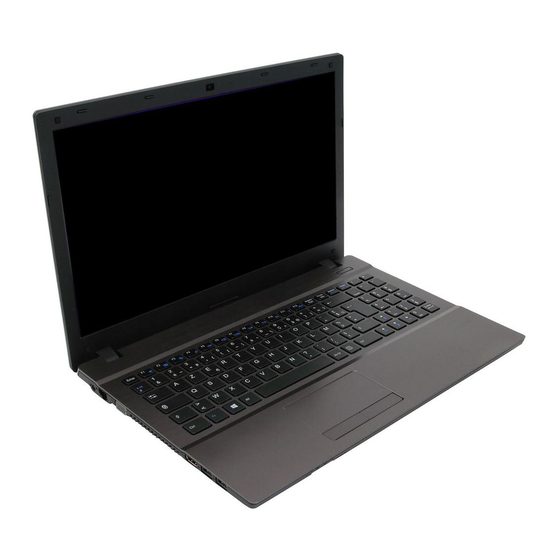
Introduction External Locator - Top View with LCD Panel Open Figure 1 Top View 1. PC Camera (Optional) 2. Built-In Microphone 3. LCD 4. Power Button 5. Keyboard 6. Touchpad & Buttons 1 - 4 External Locator - Top View with LCD Panel Open... -
Page 17: External Locator - Front & Right Side Views
Introduction External Locator - Front & Right Side Views Figure 2 Front View 1. LED Power Indicator 2. Multi-in-1 Card FRONT VIEW Reader Figure 3 Right Side View 1. Microphone-In RIGHT SIDE VIEW Jack 2. Headphone-Out Jack 3. USB 2.0 Port 4. -
Page 18: External Locator - Left Side & Rear View
Introduction External Locator - Left Side & Rear View Figure 4 Left Side View 1. DC-In Jack 2. RJ-45 LAN Jack 3. External Monitor LEFT SIDE VIEW Port 4. Vent 5. HDMI-Out Port 6. USB 3.0 Ports Figure 5 REAR VIEW Rear View 1. -
Page 19: External Locator - Bottom View
Introduction External Locator - Bottom View Figure 6 Bottom View 1. Battery 2. Component Bay Cover 3. Vent 4. Hard Disk Bay Cover 5. Speakers Overheating To prevent your com- puter from overhea- ting, make sure no- thing blocks any vent while the computer is in use. -
Page 20: Mainboard Overview - Top (Key Parts)
Introduction Mainboard Overview - Top (Key Parts) Figure 7 Mainboard Top Key Parts 1. KBC-ITE IT8518 1 - 8 Mainboard Overview - Top (Key Parts) -
Page 21: Mainboard Overview - Bottom (Key Parts)
Introduction Mainboard Overview - Bottom (Key Parts) Figure 8 Mainboard Bottom Key Parts 1. Mini-Card Connector (3G Module) 2. CPU Socket (no CPU installed) 3. Memory Slots DDR3 SO-DIMM 4. Mini-Card Connector (WLAN Module) 5. Audio Codec VIA VT1802P 6. CMOS Battery 7. -
Page 22: Mainboard Overview - Top (Connectors)
Introduction Mainboard Overview - Top (Connectors) Figure 9 Mainboard Top Connectors 1. HDMI-Out Port 2. USB Port 3.0 3. Speaker Cable Connector 4. Audio Board Cable Connector 1 - 10 Mainboard Overview - Top (Connectors) -
Page 23: Mainboard Overview - Bottom (Connectors)
Introduction Mainboard Overview - Bottom (Connectors) Figure 10 Mainboard Bottom Connectors 1. ODD Connector 2. HDD Connector 3. Power Button Cable Connector 4. Keyboard Cable Connector 5. TouchPad Cable Connector 6. Fan Cable Connector 7. Multi-in-1 Card Reader 8. External Monitor Port 9. - Page 24 Introduction 1 - 12...
-
Page 25: Disassembly
Chapter 2: Disassembly Overview This chapter provides step-by-step instructions for disassembling the W540EU series notebook’s parts and subsystems. When it comes to reassembly, reverse the procedures (unless otherwise indicated). We suggest you completely review any procedure before you take the computer apart. -
Page 26: Maintenance Tools
Disassembly NOTE: All disassembly procedures assume that the system is turned OFF, and disconnected from any power supply (the battery is removed too). Maintenance Tools The following tools are recommended when working on the notebook PC: • M3 Philips-head screwdriver •... -
Page 27: Maintenance Precautions
Disassembly Maintenance Precautions The following precautions are a reminder. To avoid personal injury or damage to the computer while performing a re- moval and/or replacement job, take the following precautions: Power Safety Warning 1. Don't drop it. Perform your repairs and/or upgrades on a stable surface. If the computer falls, the case and other Before you undertake components could be damaged. -
Page 28: Disassembly Steps
Disassembly Disassembly Steps The following table lists the disassembly steps, and on which page to find the related information. PLEASE PERFORM THE DISASSEMBLY STEPS IN THE ORDER INDICATED. To remove the Battery: To remove the 3.75G Module: 1. Remove the battery page 2 - 5 1. -
Page 29: Removing The Battery
Disassembly Removing the Battery Figure 1 Battery Removal 1. Turn the computer off, and turn it over. 2. Slide the latch in the direction of the arrow (Figure 1a a. Slide the latch and hold it 3. Slide the latch in the direction of the arrow, and hold it in place (Figure 1a in place. -
Page 30: Removing The Hard Disk Drive
Disassembly Removing the Hard Disk Drive The hard disk drive can be taken out to accommodate other 2.5" serial (SATA) hard disk drives with a height of 9.5mm Figure 2 (h). Follow your operating system’s installation instructions, and install all necessary drivers and utilities (as outlined in HDD Assembly Chapter 4 of the User’s Manual) when setting up a new hard disk. - Page 31 Disassembly 3. Lift the hard disk bay cover from point (Figure 3b Figure 3 4. Remove the hard disk bay cover (Figure 3b HDD Assembly 5. Grip the tab and slide the hard disk assembly in the direction of arrow (Figure 3c Removal (cont’d.) 6.
-
Page 32: Removing The Optical (Cd/Dvd) Device
Disassembly Removing the Optical (CD/DVD) Device Figure 4 Optical Device 1. Turn off the computer, and remove the battery (page 2 - Removal 2. Locate the component bay cover and remove screws (Figure 4a 3. Remove the component bay cover (Figure 4b a. - Page 33 Disassembly 4. Remove the screw at point (Figure 5c Figure 5 5. Use a screwdriver to carefully push out the optical device at point (Figure 5d Optical Device 6. Insert the new device and carefully slide it into the computer (the device only fits one way. DO NOT FORCE IT; The Removal (cont’d.) screw holes should line up).
-
Page 34: Removing The System Memory (Ram)
Disassembly Removing the System Memory (RAM) Figure 6 RAM Module The computer has two memory sockets for 204 pin Small Outline Dual In-line Memory Modules (SO-DIMM) supporting Removal DDRIII (DDR3) Up to 1066/1333 MHz. The main memory can be expanded up to 8GB. The SO-DIMM modules sup- ported are 1024MB and 2048MB DDRIII Modules. - Page 35 Disassembly 5. Gently pull the two release latches ( & ) on the sides of the memory socket in the direction indicated by the Figure 7 arrows (Figure 7c). The RAM module will pop-up Figure 7d , and you can then remove it RAM Module 6.
-
Page 36: Removing And Installing A Processor
Disassembly Removing and Installing a Processor Figure 8 Processor Removal Processor Removal Procedure 1. Turn off the computer, turn it over, remove the battery (page 2 - 5) and the component bay cover (page 2 - a. Locate the CPU heat sink. - Page 37 Disassembly 6. Carefully (it may be hot) remove the heat sink unit off the computer (Figure 9e Figure 9 7. Turn the release latch towards the unlock symbol to release the CPU (Figure 9f). Processor Removal 8. Carefully (it may be hot) lift the CPU up and out of the socket (Figure 9g).
- Page 38 Disassembly Processor Installation Procedure Figure 10 Processor 1. Insert the CPU (Figure 10a), pay careful attention to the pin alignment, it will fit only one way (DO NOT Installation FORCE IT!), and turn the release latch towards the lock symbol (Figure 10b).
-
Page 39: Removing The Wireless Lan Module And Keyboard
Disassembly Removing the Wireless LAN Module and Keyboard Figure 11 1. Turn off the computer, turn it over, remove the battery (page 2 - 5) and the component bay cover (page 2 - Wireless LAN 2. The Wireless LAN module will be visible at point on the mainboard and keyboard ribbon cable under the Wire- Module and less LAN module... - Page 40 Disassembly 6. Disconnect cables (Figure 12e). Figure 12 7. Remove screws from the bottom case. Keyboard Removal 8. Turn the computer over, carefully pry the top case off the bottom case at points (Figure 12g). 9. Separate the top case up and off the bottom case (Figure 11h)
- Page 41 Disassembly 10. Remove screws from the top case. Figure 13 11. Carefully lift the keyboard shielding plate Keyboard Removal 12. Carefully separate the keyboard from the top case (Figure 11d). (cont’d) i. Remove the screws. j. Lift the keyboard shield- ing plate.
-
Page 42: Removing The 3.75G Module
Disassembly Removing the 3.75G Module Figure 14 3G Module Removal 1. Turn off the computer, turn it over, remove the battery (page 2 - 12) and the component bay cover (page 2 - 10). 2. The 3.75G module will be visible at point on the mainboard (Figure 14a). -
Page 43: Removing The Ccd
Disassembly Removing the CCD Figure 15 CCD Removal 1. Turn off the computer, turn it over, and remove the battery (page 2 - 12). 2. Carefully remove the rubber screw covers and screws from the front cover (Figure 15a). a. Carefully remove 3. - Page 44 Disassembly 6. Disconnect the cable Figure 16 7. Remove the CCD module (Figure 16f). CCD Removal 8. Reverse the process to install a new CCD module. (cont’d) e. Disconnect the cable. f. Remove the CCD mod- ule. 15. CCD Module 2 - 20 Removing the CCD...
-
Page 45: Part Lists
Appendix A:Part Lists This appendix breaks down the W540EU series notebook’s construction into a series of illustrations. The component part numbers are indicated in the tables opposite the drawings. Note: This section indicates the manufacturer’s part numbers. Your organization may use a different system, so be sure to cross-check any relevant documentation. -
Page 46: Part List Illustration Location
Part List Illustration Location The following table indicates where to find the appropriate part list illustration. Table A - 1 Part List Illustration Part Location page A - 3 Bottom page A - 4 page A - 5 SATA BLU RAY COMBO page A - 6 DVD Dual Drive page A - 7... -
Page 47: Top
Figure A - 1 Top A - 3... -
Page 48: Bottom
Bottom Figure A - 2 Bottom A - 4 Bottom... -
Page 49: Sata Blu Ray Combo
SATA BLU RAY COMBO Figure A - 3 SATA BLU RAY COMBO 非耐落 SATA BLU RAY COMBO A - 5... -
Page 50: Dvd Dual
DVD DUAL Figure A - 4 DVD DUAL 非耐落 A - 6 DVD DUAL... -
Page 51: Dummy Odd
Dummy ODD Figure A - 5 Dummy ODD Dummy ODD A - 7... -
Page 52: Lcd
Figure A - 6 設變 A - 8 LCD... -
Page 53: Schematic Diagrams
Schematic Diagrams Appendix B: Schematic Diagrams This appendix has circuit diagrams of the W540EU notebook’s PCB’s. The following table indicates where to find the appropriate schematic diagram. Diagram - Page Diagram - Page Diagram - Page Table B - 1... -
Page 54: Schematic Diagrams
Schematic Diagrams System Block Diagram W540EU / W550EU VDD3,VDD5 Chief River System Block Diagram W540EU MAIN BOARD 5V,3V,5VS,3VS,1.5VS, 1.8VS,+1.5S_CPU AUDIO BOARD PHONE JACK x2, USB x1 1.8V, 0.85VS Ivy Bridge 1333/1666 MHz AUDIO BOARD 1.5V,0.75VS(VTT_MEM) PROCESSOR PHONE JACK x2, USB x2 DDR3 / 1.5V... -
Page 55: Processor 1/7-Dmi, Fdi, Peg
Schematic Diagrams Processor 1/7-DMI, FDI, PEG Ivy Bridge Processor 1/7 ( DMI,PEG,FDI ) 1.05VS U13A 20 mil PEG_IRCOMP_R 24.9_1%_04 PEG_ICOMPI PEG_ICOMPO H 22 DMI_TXN0 DMI_RX#[0] PEG_RCOMPO DMI_TXN1 DMI_RX#[1] DMI_TXN2 DMI_RX#[2] DMI_TXN3 DMI_RX#[3] PEG_RX#[0] PEG_RX#[1] DMI_TXP0 DMI_RX[0] PEG_RX#[2] DMI_TXP1 DMI_RX[1] PEG_RX#[3] DMI_TXP2 DMI_RX[2] PEG_RX#[4]... -
Page 56: Processor 2/7-Clk, Misc
Schematic Diagrams Processor 2/7- CLK, MISC Ivy Bridge Processor 2/7 ( CLK,MISC,JTAG ) Processor Pullups/Pull downs PU/PD for JTAG signals 1.05VS 1.05VS H_PROCHOT# 62_04 *51_04 XDP_TMS *51_04 XDP_TDI_R CAD Note: Use pad sharing method XDP_PREQ# H_CPUPWRGD_R *51_04 U13B 10K_04 for following clock resistor placement *51_04 XDP_TDO_R *51_04... -
Page 57: Processor 3/7- (Ddr3)
Schematic Diagrams Processor 3/7- (DDR3) Ivy Bridge Processor 3/7 ( DDR3 ) U13C U13D M_A_DQ[63:0] SA_CK[0] M_A_CLK_DDR0 9 M_B_DQ[63:0] SB_CK[0] M_B_CLK_DDR2 10 M_A_CLK_DDR#0 9 M_B_CLK_DDR#2 10 SA_CLK#[0] SB_CLK#[0] M_A_DQ0 M_B_DQ0 M_A_CKE0 9 M_B_CKE2 10 SA_DQ[0] SA_CKE[0] SB_DQ[0] SB_CKE[0] M_A_DQ1 M_B_DQ1 SA_DQ[1] SB_DQ[1] M_A_DQ2... -
Page 58: Processor 4/7- Power
Schematic Diagrams Processor 4/7- Power Ivy Bridge Processor 4/7 ( POWER ) PROCESSOR CORE POWER POWER U13F VCORE PROCESSOR UNCORE POWER 8.5A 1.05VS 8.5A AG35 AG34 VCC1 AH13 VCC2 VCCIO1 AG33 AH10 VCC3 VCCIO2 AG32 AG10 C340 VCC4 VCCIO3 AG31 AC10 AG30 VCC5... -
Page 59: Processor 5/7- Gfx Pwr
Schematic Diagrams Processor 5/7- GFX PWR Ivy Bridge Processor 5/7 ( GRAPHICS POWER ) 1.5VS_CPU POWER U13G VGFX_CORE 1K_1%_04 AT24 AK35 *AO3402L VR1_VCCGT_SENSEA 33 AT23 VAXG1 VAXG_SENSE AK34 V_SM_VREF V_SM_VREF_CNT VAXG2 VSSAXG_SENSE VR1_VSSGT_SENSEA 33 AT21 C324 C325 VAXG3 AT20 AT18 VAXG4 22u_6.3V_X5R_08 *22u_6.3V_X5R_08... -
Page 60: Processor 6/7- Gnd
Schematic Diagrams Processor 6/7- GND Ivy Bridge Processor 6/7 ( GND ) U13H U13I AT35 AJ22 VSS1 VSS81 AT32 AJ19 VSS2 VSS82 AT29 AJ16 VSS3 VSS83 VSS161 VSS234 AT27 AJ13 VSS4 VSS84 VSS162 VSS235 AT25 AJ10 VSS5 VSS85 VSS163 VSS236 AT22 VSS6 VSS86... -
Page 61: Processor 7/7- Rsvd
Schematic Diagrams Processor 7/7- RSVD Ivy Bridge Processor 7/7 ( RESERVED ) CFG Straps for Processor PEG Static Lane Reversal - CFG2 is for the 16x CFG2 1:(Default) Normal Operation; Lane # definition matches socket pin map definition U13E 0:Lane Reversed AH27 VCC_DIE_SENSE AK28... -
Page 62: Ddr3 So-Dimm_0
Schematic Diagrams DDR3 SO-DIMM_0 SO-DIMM A C141 *10p_50V_NPO_04 M_A_CLK_DDR0 M_A_CLK_D DR#0 JDIMM2A M_A_A[15:0] M_A_DQ[63:0] 4 C133 *10p_50V_NPO_04 M_A_A0 M_A_DQ0 JDIMM2B M_A_CLK_DDR1 M_A_CLK_D DR#1 M_A_A1 M_A_DQ1 M_A_A2 M_A_DQ2 M_A_A3 M_A_DQ3 1.5V M_A_A4 M_A_DQ4 M_A_A5 M_A_DQ5 VDD1 VSS16 M_A_A6 M_A_DQ6 VDD2 VSS17 M_A_A7 M_A_DQ7 VDD3... -
Page 63: Ddr3 So-Dimm_1
Schematic Diagrams DDR3 SO-DIMM_1 SO-DIMM B JDIMM1B C 106 *10p_50V_N PO_04 M_B_C LK_DD R 2 M_B_CLK_D DR #2 1. 5V JDIMM1A M_B_A[15:0] M_B_D Q[ 63:0] 4 M_B_A0 M_B_D Q0 C 104 *10p_50V_N PO_04 D Q0 M_B_C LK_DD R 3 M_B_CLK_D DR #3 M_B_A1 M_B_D Q1 D Q1... -
Page 64: Panel, Inverter, Crt
Schematic Diagrams PANEL, INVERTER, CRT PANEL CONNECTOR (30Pin & 40Pin CO-lay) PANEL POWER 3.3VS R277 2.2K_04 R276 2.2K_04 VIN_LCD J_LCD1 P_DDC_DATA P_DDC_CLK 3.3VS PLVDD BRIGHTNESS_R C292 VOUT INV_BLON 0.1u_50V_Y5V_06 C306 LVDS-LCLKN LVDS-L2N C301 LVDS-LCLKP LVDS-L2P NB_ENAVDD *1u_6.3V_X5R_04 1u_6.3V_X5R_04 LVDS-L1N NCT3522U LVDS-L1P R280 3.3VS... -
Page 65: Pch 1/9- Rtc, Hda, Sata
Schematic Diagrams PCH 1/9- RTC, HDA, SATA NO REBOOT STRAP P a n t h e r P o i n t - M ( H D A , J T A G , S A T A ) NO REBOOT STRAP: HDA_SPKR High Enable 3.3VS RTCVCC 20mils... -
Page 66: Pch 2/9- Pcie, Smbus, Clk
Schematic Diagrams PCH 2/9- PCIE, SMBUS, CLK 3.3V 2.2K_8P4R_04 PantherPoint - M (PCI-E,SMBUS,CLK) SMB_DATA SML0_CLK SMB_CLK SML0_DATA U20B 10K_8P4R_04 BG34 PEG_PCIECLKRQ7# PERN1 BJ34 BT_SBD# BT_SBD# BT_SBD# 21 PERP1 SMBALERT# / GPIO11 AV32 LPD_SPI_INTR# PETN1 AU32 SMB_CLK USB_OC#89 SMB_CLK 9,10 PETP1 SMBCLK 16,25 USB_OC#89... -
Page 67: Pch 3/9- Dmi, Fdi, Pwrgd
Schematic Diagrams PCH 3/9- DMI, FDI, PWRGD PantherPoint -M (DMI,FDI,GPIO) U20C 3.3V BC24 BJ14 DMI_RXN0 DMI0RXN FDI_RXN0 FDI_TXN0 2 BE20 AY 14 DMI_RXN1 DMI1RXN FDI_RXN1 FDI_TXN1 2 BG18 BE14 AC_PRESENT R149 10K_04 FDI_TXN2 2 DMI_RXN2 DMI2RXN FDI_RXN2 BG20 BH13 PM_SLP_LAN# R119 * 10K_04 FDI_TXN3 2... -
Page 68: Pch 4/9- Lvds, Ddi, Crt
Schematic Diagrams PCH 4/9- LVDS, DDI, CRT PantherPoint -M (LVDS,DDI) U20D AP43 BLON L_BKLTEN SD VO_TVCLKIN N AP45 Sheet 15 of 42 11,28 NB_EN AVDD L_VD D_EN SDVO_TVC LKINP AM42 L_BKLTCTL SD VO_STALLN AM40 SDVO_STALLP PCH 4/9- LVDS, Ver:1.0 P_DDC _CLK L_D DC _C LK AP39 3.3VS... -
Page 69: Pch 5/9- Pci, Usb, Rsvd
Schematic Diagrams PCH 5/9- PCI, USB, RSVD PantherPoint -M (PCI,USB,NVRAM) 3.3V R N10 10K_8P4R_04 PEG_B_C LKR Q# PEG_B_CLKRQ# USB_OC#23 U 20E USB_OC#14 Boot BIOS Strap AY 7 USB_OC#01 RSVD1 BG26 RSVD2 BBS_BIT1 BBS_BIT0 Boot BIOS Location BJ26 RSVD3 R N11 10K_8P4R_04 RSVD4 BH 25 USB_OC#1213... -
Page 70: Pch 6/9- Gpio, Cpu
Schematic Diagrams PCH 6/9- GPIO, CPU PantherPoint - M (GPIO,VSS_NCTF,RSVD) 3.3V R320 1K_04 HOST_ALERT#1 R108 1K_04 HOST_ALERT#2 3.3VS R323 *10K_04 LED_DGPU# U20F DGPU_PWROK R353 *10K_04 SATA_ODD_PWRGT S_GPIO SATA_ODD_PWRGT R356 1K_04 BMBUSY# / GPIO0 TACH4 / GPIO68 SATA_ODD_PWRGT 25 MFG_MODE R329 10K_04 R343 10K_04... -
Page 71: Pch 7/9- Pwr
Schematic Diagrams PCH 7/9- PWR PantherPoint -M (POWER) 3.3VS *15mil_s hort_06 POWER U20G 1.05VS VCCA_DAC_3.3VS 1.3A AA23 HCB1608KF-121T25 AC23 VCCCORE[1] VCCADAC C252 C266 AD21 VCCCORE[2] C261 C209 C228 C223 C246 C249 C251 C270 C273 R259 VCCCORE[3] AD23 VCCCORE[4] VSSADAC SHDN# AF21 10u_6.3V_X5R_08 1u_6.3V_X5R_04... -
Page 72: Pch 8/9 Power
Schematic Diagrams PCH 8/9 POWER PantherPoint - M (POWER) 1.05VS_VCCA_CLK *HCB1005KF-121T20 1.05VS 1.05VS POWER U20J 2.92A 3.3V C195 AD49 VCCACLK VCCIO[29] C231 0.1u_10V_X5R_04 VCCIO[30] 1u_6.3V_X5R_04 VCCDSW3_3 VCCIO[31] 3.3V C180 *0.1u_10V_X5R_04 PCH_VCCDSW 97mA DCPSUSBY P VCCIO[32] HCB1608KF-121T25 266mA VCCIO[33] VCC3_3 C190 C198 3.3VS VCC3_3[5]... -
Page 73: Pch 9/9- Gnd
Schematic Diagrams PCH 9/9- GND PantherPoint -M (GND) Voltage Rail Voltage S0 Iccmax Current (A) U20I V_CPU_IO 1.05 1 (mA) U20H AY 4 V5REF 1 (mA) AY42 VSS[159] VSS[259] VSS[0] V5REF_Sus 1 (mA) VSS[160] VSS[260] AY46 AA17 AK38 VSS[161] VSS[261] VSS[1] VSS[80] AY 8... -
Page 74: Wlan, 3G, Msata
Schematic Diagrams WLAN, 3G, MSATA 3G/MSATA MINI CARD C300 220u_6.3V_6.3*6.3*4.2 J_SIM1 SIM CONN 0.1u_16V_Y 5V_04 (TOP VIEW) *10mil_short_04 DETECT_SW UIM_MCMD UIM_PWR UIM_DATA UIM_D UIM_DATA J_3G1 *4.7K_04 60mils UIM_DATA UIM_I/O UIM_CLK UIM_C UIM_VPP WAKE# 3.3V_0 3G_3.3V UIM_CLK UIM_VPP UIM_RST *10mil_short_04 BT_DATA 1.5V_0 UIM_RST UIM_GND... -
Page 75: Ccd, Tpm, Fan, Click
TP_DATA 28 TPBUTTON_L TPBUTTON_R C410 C409 CCD, TPM, FAN, 47p_50V_NPO_04 47p_50V_NPO_04 85201-06051 CLICK TPM 1.2 CSW1~4 LIFT RIGHT TJG-532-V-T/R TJG-532-V-T/R TPBUTTON_L TPBUTTON_R W540EU 3.3VS R127 *10K_04 3.3V 6-53-3050B-042 6-53-3050B-042 C166 C170 C156 C169 12,28 LPC_AD0 LAD0 VDD1 0.1u_16V_Y5V_04 0.1u_16V_Y5V_04 0.1u_16V_Y 5V_04 1u_6.3V_X5R_04... -
Page 76: Usb3.0, Lid Switch
PCIe For transmitter and receiver the total trace length: 1"(Min)~~6"(Max). LID SWITCH IC PCIe Number of vias 4via hole(Max). PCIe clock Differential impedance 100 ohm. W540EU *BAV99 RECTIFIER 3.3V PCIe Differential pairs and pairs spacing 20mils, with Other trace spacing 25mils. -
Page 77: Card Reader (Rtl8411
*5p_50V_NPO_04 *5p_50V_NPO_04 *5p_50V_NPO_04 *5p_50V_NPO_04 Pin 3 Pin 8 Pin 41 Pin 52 Pin 61 EVDD10 EVDD10 VDDREG VDDREG 4 IN 1 SOCKET SD/MMC/MS/MS Pro W540EU W550EU Co-lay 3/28 J_CARD-REV1 J_CARD-REV2 SD_CD# SD_CD# CD_SD CD_SD C403 C408 C428 C429 SD_D2 SD_D2... -
Page 78: Sata Odd, Led, Usb Charge
Schematic Diagrams SATA ODD, LED, USB CHARGE BAT LED POWER ON LED SATA ODD Zero Power ODD LED_BAT_CHG LED_PWR 28 LED_BAT_FULL LED_ACIN 28 5VS_ODD ¹q®e½Ð¾aªñJ_ODD1 J_ODD1 RN17 C359 0.01u_16V_X7R_04 PJ23 *OPEN-3mm 220_8P4R_04 SATA_TXP2 12 C357 0.01u_16V_X7R_04 Pin swap 3/30 SATA_TXN2 12 C356 0.01u_16V_X7R_04 SATA_RXN2 12... -
Page 79: Hdmi, Rj45
Schematic Diagrams HDMI, RJ45 FOR W/O LEVEL SHIFT RN16 *0_8P4R_04_SHORT LAN PORT HDMIC_C0CP_C TMDS_DATA2-L HDMIC_C0CN_C TMDS_DATA2#-L HDMIC_C1CP_C TMDS_DATA1-L 3.3VS HDMIC_C1CN_C TMDS_DATA1#-L 3/23 LAN_MDIN0 LMX1- Q16A RN15 LAN_MDIN0 TD4- MX4- LAN_MDIP0 LMX1+ MTDK5S6R *0_8P4R_04_SHORT LAN_MDIP0 TD4+ MX4+ LAN_MDIN1 LMX2- LMX1+ DLMX1+ HDMIC_C2CP_C TMDS_DATA0-L LAN_MDIN1... -
Page 80: Audio Codec Vt1802P
Schematic Diagrams AUDIO CODEC VT1802P CODEC (ALC269 & VT1802P) PVDD1_2 R400 La yout note: *15mil_short_06 EMI Require R452 *0_06 GND and AUDG space is 1.5V 60m ils ~ 100mils 3/23 DVDD_IO C431 C425 For 1.5V HDA Link. 20 mil *HCB1005KF-121T20 R420 *28mil_short_06 0.1u_16V_Y 5V_04... -
Page 81: Kbc-Ite It8518E
Schematic Diagrams KBC-ITE IT8518E KBC_AVDD HCB1005KF-121T20 VDD3 VDD3 VDD3 C158 C159 C160 C185 C203 C174 C173 C165 *0.1u_16V_Y5V_04 10u_6.3V_X5R_06 0.1u_16V_Y5V_04 0.1u_16V_Y 5V_04 0.1u_16V_Y 5V_04 *0.1u_16V_Y 5V_04 *0.1u_16V_Y 5V_04 R155 C172 100K_04 0.1u_16V_Y5V_04 KBC_AGND *28mil_short_06 EC_VCC KBC_WRESET# 3.3VS 3/23 C178 J_KB1 85208-24051 1u_6.3V_X5R_04 KB-SI0... -
Page 82: 5Vs, 3Vs, 1.5Vs Cpu
Schematic Diagrams 5VS, 3VS, 1.5VS CPU VIN1 DD_ON PR97 100K_04 VIN1 DDON_LATCH PR96 *100K_04 USB_CHARGE_EN 28,30 DD_ON_LATCH PR173 1K_04 PWR_SW#_R PR99 10K_04 M_BTN# VDD3 M_BTN# PWR_SW# USB_CHARGE_EN R331 *1K_04 PR98 1K_04 INSTANT-ON PWR_SW# 28 R332 *100K_04 P2808B0 ¹w¯dPJ17¡Acost down 5V MOS W USB Charge ¤W¥ó... -
Page 83: Vdd3, Vdd5
Schematic Diagrams VDD3, VDD5 VREF_VDD PR93 *0_04 PR90 *20mil_04 PC49 3/29 1u_10V_Y 5V_06 VFB2 VFB1 PR175 PR88 3/29 EN_3V EN_5V PC151 110K_1%_04 110K_1%_04 PC152 1000p_50V_X7R_04 1000p_50V_X7R_04 VREG3 PC59 PC58 PC153 PR176 *10K_04 4.7u_25V_X5R_08 4.7u_25V_X5R_08 5608POK VDD3 LDO3 SY S5V VDD5 1u_10V_Y 5V_06 PC56 PC61... -
Page 84: Power 0.85Vs, 1.8Vs
Schematic Diagrams Power 0.85VS, 1.8VS -n²¾¾aªñPIN6¸} 1.8VS 3 .3V PC147 V1.8 2.2u_6.3V_X5R_06 1.8VS PR84 10K_04 3.3V VCN TL PJ22 1.8VS_PWR GD POK_6610 *10mil_short_04 14,29 1.8VS_PWR GD VOUT *OPEN -3mm VOUT PR83 10K_04 EN1.8VS1 PC142 PC 143 PC144 PC45 VFB_6610 PR85 1.3K_1%_04 GN D PQ35... -
Page 85: Power 1.5V/1.05Vs
Schematic Diagrams POWER 1.5V/1.05VS PD20 PC171 PC170 PC168 PC169 PQ43 RB0540S2 ME4894-G VDDQ VTT_MEM PC172 1.5V 10u_6.3V_X5R_06 VBST PC173 0.1u_10V_X7R_04 VLDOIN VBST VDDQ PJ26 PL13 PR111 DRVH TMPC 1004H-1R0M-Z01 PJ24 VTT_MEM DR VH 3.3_06 1.5V *OPEN-2mm PR192 PC167 *OPEN-8mm PC176 PC175 PC174 VTTGND... -
Page 86: Power Vcore1
Schematic Diagrams POWER VCORE1 PC 21 0.1u_10V_X7R_04 R T4 PUT COLSE TO GT PR41 24K_1%_04 CSCOMPA CSREFA PR158 PC27 1000p_50V_X7R_04 Inductor 165K_1%_04 PR148 1.6K_1%_04 PR159 PC122 PC 113 10p_50V_NPO_04 1.05VS PUT COLSE TO CPU 10_1%_04 33p_50V_NPO_04 PR156 PC 120 3/29 SOCKET PR26 *75_04... -
Page 87: Power Vcore2
Schematic Diagrams POWER VCORE2 3/28 PC81 PC92 PC88 PC127 PQ18 MDU1516 3/23 3/28 PR131 *28m il_short_06 HG_1 PC134 PC31 PC 30 PC28 DCR 1.1mohm Sheet 34 of 42 SW 1 MDU1516 SW 1 VCORE 0.36UH_12.9*14*3.8 PQ23 POWER VCORE2 MDU1512 PQ22 3/23 MDU1512 PD14... -
Page 88: Ac In, Charger
*10mil_short_04 BAT_DET IACM IACP COMP PC95 IACP COMP JBATTA2 PQ17 PC94 AC AV 2SK3018S3 PR11 100K_04 53022-00571-001 ACAV VDDA PR136 W540EU PR10 PR18 *20mil_04 PR28 0_04 *0_04 *15mil_short_06 PR12 PC86 PC107 PC108 PC104 PR128 *20mil_04 SMC_BAT_R 28 *1u_25V_08 *1u_25V_08 1u_25V_Y5V_08... -
Page 89: Audio Board
Schematic Diagrams AUDIO BOARD USB PORT A_USBVCC 60 mil 0.1u_16V_Y5V_04 AJ_USB1 Port3 AGND AUSB_PN1 AUSB_PN1_R DATA_L AUSB_PP1 AUSB_PP1_R DATA_H *WCM2012F2S-SHORT D02A Change footprint US04036BCA081 6-21-B49C0-104 6-21-B49B0-104 AGND TO M/B AUDIO JACK Sheet 36 of 42 AUDIO BOARD AJ_MIC1 AMIC_SENSE AMIC1-R FCM1005KF-121T03 AMIC1-L FCM1005KF-121T03... -
Page 90: Audio Board (W550Eu
Schematic Diagrams AUDIO BOARD (W550EU) USB PORT AA_USBVCC AA_USBVCC 60 mil 60 mil AAC3 AAC2 AAC15 AAC16 AAC4 AAC17 *0.1u_16V_Y 5V_04 *0.1u_16V_Y 5V_04 Port3 Port4 AAJ_USB1 AAJ_USB2 AAGND AAGND AAUSB_PN1 AAL6 AAUSB_PN1_R AAUSB_PN2 AAL8 AAUSB_PN2_R DATA_L DATA_L AAUSB_PP1 AAUSB_PP1_R AAUSB_PP2 AAUSB_PP2_R DATA_H DATA_H... -
Page 91: Lid Sw Board (W550Eu
Schematic Diagrams LID SW BOARD (W550EU) LID SWITCH BOARD Sheet 38 of 42 LID SW BOARD L_3.3V (W550EU) LJ_LID1 L_LID_SW# *85204-03001 L_GND For 15" L_3.3V L_U1 L_LID_SW# L_C1 *0.1u_16V_Y5V_04 *MH248-ALFA-ESO H2_3B5_0D2_3 C43D43 C43D43 L_GND L_GND 6-02-00248-LC2 6-02-00268-LC1 L_GND LID SW BOARD (W550EU) B - 39... -
Page 92: Power Sw Board
Schematic Diagrams POWER SW BOARD POWER SW & LED S_3.3VS POWER SWITCH 220_04 20mil Z4301 Sheet 39 of 42 *0.1u_16V_Y 5V_04 SJ_SW1 POWER SW SMGND SMGND SM_BTN# RY -SP150DBW71-5A S_3.3VS BOARD 20mil 6-52-56001-023 3/28 6-52-56001-028 85201-04051 6-52-56000-020 6-52-56001-022 SMGND SMH1 6-53-3050B-042 POWER BUTTON SPWR_SW1... -
Page 93: External Odd Board
Schematic Diagrams EXTERNAL ODD BOARD ODD BOARD FROM M/B TO ODD QJ_ODD1 QJ_ODD2 Q_SATA_TXP1 Q_SATA_TXN1 Q_SATA_RXN1 Sheet 40 of 42 Q_SATA_RXP1 EXTERNAL ODD QGND QGND BOARD Q_ODD_DETECT# Q_5VS Q_5VS Q_SATA_ODD_DA# *242003-1 *202001-1 P IN P IN QGND QGND G ND1 ~2 =WG ND G ND1 ~3 =Q G ND 6-21-14030-013 6-21-13010-013(DIP) -
Page 94: Power Diagram
Schematic Diagrams Power Diagram 3.3V 1.05VS 2.92A PWR SW B'd M_BTN# RTCVCC 3.3VS VCORE 1.05VS_VTT 1.5VS 1.05VS_VTT Cougar 8.5A 3.3VS VDD3 Point VGFX_CORE 1.5V ALL_SYS_PWRGD RSMRST# SO-DIMM 1.8VS RSMRST#, PMSYS_PWRGD_BUF 1.2A PWR_SW# DPWROK DRAMPWROK SM_DRAMPWROK IT8518 PWR_BTN# 1.5VS_CPU P2808B PWRBTN# H_CPUPWRGD PM_PCH_PWROK PWOCPWRGD... -
Page 95: Power On Seq
Schematic Diagrams Power On SEQ POWER ON SEQUENCE M_BTN# M_BTN# 506ms DD_ON DD_ON 28ms 1.2ms 3.3V 3.3V 2.4ms RSMRST# RSMRST# 100ms PWR_BTN# PWR_BTN# 52ms 200ms SUSC# SUSC# 218ms 1.5V 1.2ms Sheet 42 of 42 1.5VS_CPU 1.24ms Power On SEQ SUSB# SUSB# 32us 1.5VS... - Page 96 Schematic Diagrams B - 44...
-
Page 97: Updating The Flash Rom Bios
Download the BIOS computer model. 1. Go to www.clevo.com.tw and point to E-Services and click E-Channel. Note that BIOS versions 2. Use your user ID and password to access the appropriate download area (BIOS), and download the latest BIOS files... -
Page 98: Use The Flash Tools To Update The Bios
BIOS Update Use the flash tools to update the BIOS 1. Make sure you are not loading any memory management programs such as HIMEM by holding the F8 key as you see the message “Starting MS-DOS”. You will then be prompted to give “Y” or “N” responses to the programs being loaded by DOS.
Need help?
Do you have a question about the W540EU and is the answer not in the manual?
Questions and answers