Table of Contents
Advertisement
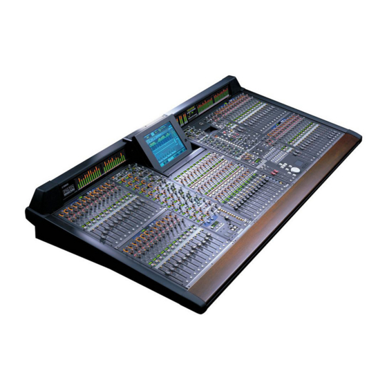
CONTROL SURFACE
SERVICE MANUAL
CONTENTS
REVISED PAGE LIST ··························································· 2-1
SPECIFICATIONS································································· 3-1
PANEL LAYOUT···································································· 3-3
CONNECTOR CIRCUIT DIAGRAM ········································· 4
DISASSEMBLY PROCEDURE··············································· 15
LSI PIN DESCRIPTION ·························································· 31
IC BLOCK DIAGRAM ····························································· 39
CIRCUIT BOARDS ································································· 45
INSPECTION ·········································································· 98
TEST PROGRAM ································································· 103
BLOCK DIAGRAM ································································ 126
PARTS LIST
CIRCUIT DIAGRAM
PA
011508
HAMAMATSU, JAPAN
****
Copyright (c) Yamaha Corporation. All rights reserved. PDF-K-
'01.03
Advertisement
Table of Contents

Related Manuals for Yamaha CS1D


Summary of Contents for Yamaha CS1D
-
Page 1: Table Of Contents
LSI PIN DESCRIPTION ·························································· 31 IC BLOCK DIAGRAM ····························································· 39 CIRCUIT BOARDS ································································· 45 INSPECTION ·········································································· 98 TEST PROGRAM ································································· 103 BLOCK DIAGRAM ································································ 126 PARTS LIST CIRCUIT DIAGRAM 011508 HAMAMATSU, JAPAN **** Copyright (c) Yamaha Corporation. All rights reserved. PDF-K- '01.03... - Page 2 CS1D REVISED PAGE LIST ITEM PAGE ITEM PAGE SPECIFICATIONS PNC1 CONNECTOR CIRCUIT DIAGRAM 4,5,6,8,10 CUTBVL2,HMVOLA2,HMVOLB2 11,13,14,14a DRL,DRN,DRS,PHNAB2 DISASSEMBLY PROCEDURE 18~23,25 LSI PIN DESCRIPTION IC BLOCK DIAGRAM 39, 40 PNM1 72,73 CIRCUIT BOARDS (45~97) PNOS4 STO1,STO2,PS2HP MSCPU MTCPU 46, 47 PONOS2,PNOS5...
- Page 3 CS1D < CIRCUIT DIAGRAM > ITEM PAGE ITEM PAGE MB21 CIRCUIT DIAGRAM CNDS3 CIRCUIT DIAGRAM MB22 CIRCUIT DIAGRAM ADA2 CIRCUIT DIAGRAM MIO CIRCUIT DIAGRAM PNC2 CIRCUIT DIAGRAM CIO1 CIRCUIT DIAGRAM PCIF CIRCUIT DIAGRAM STI CIRCUIT DIAGRAM AEI CIRCUIT DIAGRAM STO1 CIRCUIT DIAGRAM...
- Page 4 IMPORTANT NOTICE This manual has been provided for the use of authorized Yamaha Retailers and their service personnel. It has been assumed that basic service procedures inherent to the industry, and more specifically Yamaha Products, are already known and understood by the users, and have therefore not been restated.
-
Page 5: Specifications
CS1D SPECIFICATIONS Number of scene memories 990 Stereo/group assign STEREO/MIX 1–48 (FIX/VARI Sampling Frequency Intermal: 48 kHz/44.1 kHz selectable) External: 44.1 kHz -10 %–48 kHz +6 % Metering pre att peak, comp/gate gain reduction, Fader 64 x 100 mm motorized... - Page 6 CS1D ANALOG INPUT CHARACTERISTICS Input level Input Actual Load For Use With GAIN Connector Terminals Impedance Nominal Nominal Max. before clip -44 dB 50–600 Ω Mics & -44 dB (4.89 mV) -30 dB (24.5 mV) TALKBACK IN XLR-3-31 type 3 kΩ...
-
Page 7: Panel Layout
DC POWER INPUT – DC 60 V KN-27-32S 27pin Connector (Female) LCD Display 800 x 600 Dots Graphic color LCD with backlit PCMCIA card slot for external memory PW1D Power Supply to the CS1D PANEL LAYOUT Note: See operation manual for details. -
Page 8: Connector Circuit Diagram
CS1D CONNECTOR CIRCUIT DIAGRAM KEC-92541-2... - Page 9 CS1D MTCPU STO1 MB21 CN101 STO2 CNDS1 KEC-92541-3...
- Page 10 CS1D MB22 LMY4AD AD2 MO1-2 MO2-2 ADA2 PCIF CNDS2 from MB23(CN109) from MB23(CN108) KEC-92541-4...
- Page 11 CS1D CMU2 CMU1 CCAS PNC1 MB23 PNC2 CNDS3 KEC-94541-5...
- Page 12 CS1D PS2HP LAMPVR ( 3 ) CN101 CN102 ( 2 ) CN101 CN102 CN101 CN102 ( 1 ) CN101 CN102 CN101 CN102 LCDC LCDIF KEC-92541-6...
- Page 13 CS1D PNM1 PNM2 PNM2 PNM2 PNM2 PNM2 PNM2 PNM2 PNM2 PNM2 PNM2 PNM2 PNM2 PNM3 PNM3 MSCPU PNM4 KEC-94541-7...
- Page 14 CS1D PNOS2 PNI2 PNI2 PNOS5 PNOS5 HMVOLA2 PNOS6 PNOS4 HMVOLB2 PNOS4 PNOS3 CUTBVL2 CRDC1 PNOS1C PNI2 CRDC2 PNI2 PNOS1R OSCPU PNOS1L TB1CAN2 TB1-2 TPSW KEC-92541-8...
- Page 15 CS1D • ASSY CONTROL PANEL INSEL FADER CN11 CN17 CNY1 PNIS4 CN16 CNX1 PNIS3 CN15 CN805 CN14 CN801 CN803 CN10 CN804 CN802 PNIS2 CN12 CN804 CN13 CN803 CN800 CN802 CN801 ISCPU PNIS1 CN300 CN301 CN302 CN303 CN304 CN305 PHNAB2 KEC-92541-9...
- Page 16 CS1D PNI1 PNI2 PNI2 PNI2 PNI2 PNI2 PNI2 PNI2 PNI2 PNI2 PNI2 PNI2 PNI2 INCPU KEC-94541-10...
-
Page 17: Circuit Boards
CS1D Circuit Board CN No. Pin No. Circuit Board CN No. Pin No. PW1D – Bottom Assembly PW1D 1,2,4–10 POWER UNIT CN28 1–9 (INPUT A) 11–20 CN29 1–10 22–24 CN24 1–3 26–27 CN20 1–2 PW1D 1,2,4–10 POWER UNIT CN26 1–9 (INPUT B) 11–20... - Page 18 CS1D Circuit Board CN No. Pin No. Circuit Board CN No. Pin No. Bottom Assembly – Bottom Assembly POWER UNIT 1–3 CS CNDS1 CN10 1–3 4–6 CS CNDS3 CN60 1–3 1–3 CS CNDS1 CN10 4–6 4–6 CS CNDS3 CN60 4–6...
- Page 19 CS1D Circuit Board CN No. Pin No. Circuit Board CN No. Pin No. Meter Assembly – Meter Assembly CANNON CONECTOR 3–4 CS DRN CN101 1–2 CANNON CONECTOR 3–4 CS RDS CN101 1–2 Assembly – LCD Assembly LCD-BACKLIGHT 1–2 CS LCDC CN401 1–2...
-
Page 20: Disassembly Procedure
CS1D DISASSEMBLY PROCEDURE Control Panel Assembly Remove the following screws, each name plate, under plate. The control panel assembly can then be removed. (Fig. 1) Parts and Assembly Ref. No. Screw Name plate MASTER 680D Bolt 3.0x6 MFZNBL (V4750100) Name plate IN SEL 680C Bolt 3.0x6 MFZNBL (V4750100) - Page 21 CS1D Remove the nine (9) screws marked [150]. The CS PNM1 circuit board can then be removed. Remove the switch knobs marked [A] on the circuit board. (Fig. 3) Fader Assembly, CS PNM2 Circuit Board Remove the control panel assembly (MASTER).
- Page 22 CS1D [280] Control panel master Switch knob C [280] Switch knob A x36 Switch knob A x24 [280] Switch knob C [280] Encoder knob x36 Switch knob B x12 [330] Switch knob B x12 Switch knob D [220] x24 [330] Fader knob x12 [220]: Flat Head Screw 3.0 x 6 MFZN2BL (EC030030)
- Page 23 CS1D [ 247B ] [ 247A ] CS PNIS3 [ 190 ] CS PNIS4 [170A] [ 170B ] x10 Fader Assembly [ 170A ] [ 190 ] CS PNIS2 CS ISCPU CS PNIS1 [ 490 ] CS PHNAB2 [ 190 ] Protect,P.C.B.
- Page 24 CS1D PHNAB2 Circuit Board 11-1 Remove the control panel assembly (IN SEL). (See Procedure 1.) 11-2 Remove the four (4) screws marked [500]. (Fig. 4) 11-3 Remove the two (2) hexagonal nuts marked [490]. The CS PHNAB2 circuit board can then be removed.
- Page 25 CS1D Fader Assembly, CS PNI2 Circuit Board 14-1 Remove the control panel assembly (IN12, IN24, IN36, IN48). (See Procedure 1.) 14-2 Remove the fader knob. (Fig. 5) 14-3 Remove the two (2) screws marked [210]. The fader assembly can then be removed. (Fig. 5) 14-4 Remove the screw marked [205].
- Page 26 CS1D Encoder knob D Knob C Encoder knob A PCMCIA assembly [ 440B ] Hexagonal nut C [ 440A ] Spacer Fader knob A [ 380A ] Encoder knob B [ 380A ] Fader knob A Knob A Hexagonal nut A...
-
Page 27: Circuit Board
CS1D HMVOLB2 Circuit Board 20-1 Remove the control panel assembly (OUT SEL). (See Procedure 1.) 20-2 Remove the two (2) knobs marked [C]. 20-3 Remove the two (2) hexagonal nuts marked [C]. The CS HMVOLB2 circuit board can then be removed. (Fig. 6, Fig. 7) - Page 28 CS1D 25-3 Remove the hexagonal nut marked [D]. The encoder assembly can then be removed. (Fig. 6, Fig. 7) CS PNOS6 Circuit Board 26-1 Remove the control panel assembly (OUT SEL). (See Procedure 1.) 26-2 Remove the five (5) screws marked [880]. The CS PNOS6 circuit board.
- Page 29 CS1D LCD Assembly 31-1 Remove the three (3) bolts marked [370] and the three (3) bolts marked [470]. The Upper LCD Escutcheon and the Lower LCD escutcheon can then be removed. (Fig. 9) 31-2 Remove the two (2) screws marked [450]. The LCD hinge cover can then be removed.
- Page 30 CS1D CS CNDS2 Circuit Board 35-1 Remove the control panel assembly (MASTER). (See Procedure 1.) 35-2 Remove the nine (9) screws marked [820]. The CS CNDS2 circuit board can then be removed. (Fig. 11) ADA2 Circuit Board 36-1 Remove the control panel assembly (OUT SEL).
- Page 31 CS1D Rear Panel Assembly (A), (B), (C) 38-1 Remove the following screws, each rear panel can then be removed. (Fig. 12) Parts Ref. No. Screw Rear panel A 990c Bind Head Tapping Screw-B A4.0x8 MFZN2BL (VC688800) Rear panel B 1010c Bind Head Tapping Screw-B A4.0x8 MFZN2BL (VC688800)
-
Page 32: Power Supply Unit
CS1D CS DRL Circuit Board 43-1 Remove the CANNON assembly. (See Procedure 42.) 43-2 Remove the two (2) screws marked [C50]. The CS DRL circuit board can then be removed. (Fig. 13) CS MT1, CS MT2, CS MT3 Circuit Board 44-1 Remove the rear panel (A), (B) and (C). - Page 33 CS1D [ 806 ] [ 806 ] Power Supply Unit [806]: Bind Head Tapping Screw-B A4.0x8 MFZN2BL (VC688800) Fig. 15 CARD Assembly (Rear Panel C) 47-1 Remove the rear panel (C). (See Procedure 38.) 47-2 Remove the following screws, each assembly can then be removed.
- Page 34 CS1D CS MB21, MB22 Circuit Board 49-1 Remove the Control Panel Assembly (IN SEL, IN12, IN24). (See Procedure 1.) 49-2 Remove the rear panel (A). (See Procedure 38.) 49-3 Remove all the CARD assembly in the procedure 45. 49-4 Remove the two (2) screws marked [450] and the the four (4) screws marked [460].
- Page 35 CS1D CS PCIF Circuit Board 51-1 Remove the Control Panel Assembly (OUT SEL). (See Procedure 1.) 51-2 Remove the eight (8) screws marked [880]. The PC assembly can then be removed. (Fig. 11) 51-3 Remove the five (5) screws marked [30], the three (3) screws marked [50] and the four (4) screws marked [A].
-
Page 36: Lsi Pin Description
CS1D LSI PIN DESCRIPTION YM3436DK (XG948E0) DIR2 (Digital Format Interface Receiver)············································· 31 YM3437C-F (XM530A00) DIT2 (Digital Format Interface Transmitter) ······································ 31 HD6477042AF28 (XY715A00) CPU ························································································· 32 AK4393-VS-E2 (XW029A00) DAC (Digital to Analog Converter) ·············································· 32 HD6437043AF33 (XY138A00) CPU ·························································································· 33 µPD71051GB-3B4 (XI999A00) USART(Synchronous Asynchronous Receiver Transceiver) ··... - Page 37 CS1D HD6477042AF28 (XY715A00) CPU NAME FUNCTION NAME FUNCTION PE14 Port E PE15 Port E Data bus Ground Ground Data bus Power supply Address bus Data bus Ground XTAL Crystal oscillator Mode control EXTAL Crystal oscillator Mode control Non-maskable interrupt request...
- Page 38 CS1D HD6437043AF33 (XY138A00) CPU NAME FUNCTION NAME FUNCTION /WRHH HH write DAM transfer strobe/Port E /DACK0/PE14 Data bus /WRHL HL write CASHH/PA21 HH Column address strobe/Port A DACK1/PE15 DMA transfer strobe/Port E Power supply Ground Data bus Ground Address bus...
- Page 39 CS1D µPD71051GB-3B4 (XI999A00) USART (Synchronous Asynchronous Receiver Transceiver) NAME FUNCTION NAME FUNCTION No connection No connection Serial data output Master clock Data bus Reset No connection No connection /DSR Data set ready Data bus /RTS Request to send /TXCLK Transmitting clock...
- Page 40 CS1D SGH609080F-47F (XU235A00) ATSC NAME FUNCTION NAME FUNCTION syncati Synch. word input terminal for ati, synci Synch. word input terminal for si3-0 input siat3-0 input mccti 64 fs clock input terminal for ati, mcci 64 fs clock input terminal for si3-0 input...
- Page 41 CS1D AK5392-VS-E2 (XV065A00) ADC (Analog to Digital Converter) NAME FUNCTION NAME FUNCTION VREFL L ch standard voltage output (+3.75 V) SDATA Serial data output GNDL L ch Ground FSYNC Frame synchronization clock VCOML L ch common voltage (+2.5 V) MCLK Master clock input CMODE=“H”:384 fs...
- Page 42 CS1D YSS904-F (XV989A00) DSP5 (Digital Signal Processor) NAME FUNCTION NAME FUNCTION Not used Not used Ground SIO28 Power supply SIO29 Serial data bus System master clock input (60 MHz or 30 MHz) SIO30 System master clock output (High or 30 MHz)
- Page 43 CS1D TPS2205IDB (XW602A00) Power Controller NAME FUNCTION NAME FUNCTION Card power (5 V) 3.3V Card power (3.3 V) Card power (5 V) 3.3V Card power (3.3 V) A_PGM AVPP voltage control Overflow control ("L" level signal output) A_Vcc AVPP voltage control...
-
Page 44: Ic Block Diagram
CS1D IC BLOCK DIAGRAM HD74LV02AFPEL (IS000200) HD74LV04AFPEL (IS000400) HD74LV08AFPEL (IS000800) Quad 2 Input NOR HD74LS06FPEL (XH610A00) Quad 2 Input AND SN74LS06NSR (XP985A00) Hex Inverter HD74LV11AFPEL (IS001100) HD74LV14AFPEL (IS001400) HD74HC30FPTL (XQ970A00) Triple 3 Input AND Hex Inverter 8 Input NAND HD74LV32AFPTL (IS003200) - Page 45 CS1D HD74LV125AFPEL (IS012500) SN74LV138ANSR (IS013810) SN74LV139ANSR (IS013910) Quad 3-State Bus Buffer 3 to 8 Demultiplexer Dual 2 to 4 Demultiplexer Select Output Enable Output SN74LV164ANSR (IS016410) HD74LV244AFPEL (IS024400) HD74LV245AFPEL (IS024500) 8-Bit Shift Register Octal 3-State Bus Buffer TC74VHCT245AF (XV242A00) TC74VHC245F (XT487A00)
- Page 46 CS1D SN75124NSR (XV930A00) SN75C1168NSR (XU073A00) SN74LV4052ANSR (IS405210) Triple Line Receiver Line Driver / Receiver Differential 4-Channel Multiplexer/Demultiplexer Y-COM Y-COM X-COM X-COM TC74LVX4245FS (XU229A00) AM26LS31CNSR (XU996A00) DS26C32ATM (XQ544A00) Dual Supply Octal Bus Transceiver Quad Line Driver Quad Differential Line Receiver VCCA...
- Page 47 CS1D TC74HC238AF (XT163A00) 3 to 8 Line Decoder Select Inputs Enable Data Inputs Output TA7291S (XF557A00) Motor Driver DRIVER Vref OUT1 Heat OUT2 OUT1 OUT2 protector Vref TB62705CF (XV013A00) LED Driver OUT 0 OUT 1 OUT 7 I - REG.
- Page 48 CS1D TD62M8600F (XV014A00) MAX202CSE (XP113A00) Source Driver RS-232C Transceiver +5V INPUT 0.1uF 0.1uF 6.3V 0.1uF +5V TO +10V 6.3V C1– VOLTAGE DOUBLER OUT1 OUT8 +10V TO –10V 0.1uF V– T3 OUT T4 OUT VOLTAGE INVERTER 0.1uF C2– T1 OUT T5 IN...
-
Page 49: Mtcpu
CS1D AD1890JP (XV453A00) 917090 (XK866A00) ASRC – SERIAL IN SERIAL OUT WCLK - I WCLK - O – – LR - I LR - O ACCUM DATA - O MULT FIFO COEF ROM BKPOL - I –IN CLOCK TRGLR - I... -
Page 50: Circuit Boards
CS1D CIRCUIT BOARDS STO1 Circuit Board to STO2-CN101 Component side STO2 Circuit Board PS2HP Circuit Board to STO1-CN2 MONITOR B MONITOR A KEYBOARD MOUSE to ADA2-CN302 to PCIF-CN305 Component side Component side Pattern side STO1,STO2: 3NA-V504660 PS2HP: 3NA-V454540... - Page 51 to MO2_2-CN604 to MO1_2-CN405 to MB21-CN1 to MO2_2-CN602 to CNDS1-CN100 to PN2-CN109 to MT2-CN1 to MT2-CN2 to MT1-CN2 to MO1_2-CN400 to ADA2-CN303 to MB22-CN503 to MB21-CN4 to MB21-CN5 to MB21-CN6...
-
Page 52: Mtcpu
CS1D MTCPU Circuit Board Pattern side 3NA-V411320... - Page 53 to CNDS2-CN203 to MTCPU-CN13 to LMY4AD-AD2-CN500 to STI-CN200 to CIO-CN2 to MIO-CN100 to MIO-CN100 to CNDS1-CN103 to STO1-CN1 to AE1-CN1 to CIO-CN2 to MIO-CN100 to MIO-CN100 to MTCPU-CN10 to MTCPU-CN12 to MTCPU-CN14...
- Page 54 CS1D MIO Circuit Board Component side Pattern side 3NA-V438190...
- Page 55 CS1D CIO Circuit Board Component side Pattern side 3NA-V438180...
- Page 56 CS1D STI Circuit Board Component side Pattern side 3NA-V411300...
- Page 57 CS1D AEI Circuit Board Component side Pattern side 3NA-V438150...
-
Page 58: Mb22
CS1D CNDS2 Circuit Board Component side to Power unit-CN19 CN206: to ISCPU-CN11 CN30: to Power unit-CN7 CN39: to MO1 _ 2-CN404 CN31: to Power unit-CN8 CN40: to Power unit-CN39 CN207: to MT3-CN5 CN312: CN32: to Power unit-CN34,35 CN41: to Power unit-CN15,16... -
Page 59: Cnds1,Lampvr,Lcdc
CS1D CNDS1 Circuit Board to INCPU-CN5 to INCPU-CN4 to MB21-CN3 to MB21-CN2 to MTCPU-CN201 from Power unit from Power unit from Power unit from Power unit -CN5,6 -CN11,12 -CN13,14 -CN23 from Power unit from Power unit from Power unit -CN34,35... - Page 60 CS1D PNC2 Circuit Board to ISCPU-CN3 to CNDS3-CN500 to OSCPU-CN17 to INCPU-CN1 to MTCPU-CN1 to INCPU-CN1 to MSCPU-CN31 to INCPU-CN1 Component side Pattern side PNM4 Circuit Board to MSCPU-CN30 Component side PNC2: 3NA-V454540 PNM4: 3NA-V445280...
- Page 61 to TB1_2-CN703 to MO2_2-CN606 to CUTBVL2-CN504 to MTCPU-CN3 to TB1_2-CN702 to CNDS2-CN317 to CNDS2-CN319 to MO2_2-CN601 to CNDS2-CN316 to HMVOLB2-CN203 to PHNAB2-CN300...
- Page 62 CS1D MO1-2 Circuit Board MO2-2 Circuit Board MONITOR OUT ANALOG TALKBACK IN 2 CUE OUT ANALOG to MTCPU-CN8 to ADA2-CN103 to ADA2-CN100 to MTCPU-CN16 to CNDS2-CN312 to MTCPU-CN4 to MTCPU-CN15 Component side Component side MO1-2, MO2-2: 3NA-V667340 56-b...
-
Page 63: Pcif
CS1D CNDS3 Circuit Board from Power unit from Power unit from Power unit -CN11,12 -CN19 -CN17,18 from Power unit from Power unit from Power unit from Power unit -CN37,38 -CN5,6 -CN34,35 -CN13,14 to INCPU-CN5 to INCPU-CN4 to MB23-CN113 to MB23-CN114... - Page 64 to LCDIF-CN302 to TPSW-CN101 to CRDC1-CN101 to CRDC1-CN105 to LCDIF-CN301 to LCDIF-CN303 REMOTE NUM KEY MOUSE KEY BOARD SVGA OUT RS-422...
-
Page 65: Pcif
CS1D PCIF Circuit Board Pattern side 3NA-V451420... -
Page 66: Pnis3,Pnm3
CS1D LMY4AD Circuit Board PNIS3 Circuit Board 2-TRACK IN ANALOG to ISCPU-CN16 Component side Pattern side PNM3 Circuit Board to MSCPU-CN29 Component side MSCPU-CN46 LMY4AD: 3NA-V491400 to MB22-CN502 PNIS3: 3NA-V411140 Component side PNM3: 3NA-V445280... - Page 67 CS1D MTG Circuit Board TIME CODE IN to CMU2-CN105 to CMU2-CN104 Component side Pattern side MT1 Circuit Board to MT2-CN3 to MT3-CN1 to MT2-CN4 to MT3-CN2 to MTCPU-CN7 to CNDS2-CN202 Component side MTG: 3NA-V454540 MT1: 3NA-V433370...
- Page 68 CS1D CMU1 Circuit Board PC CONTROL RC-232-C to MB23-CN106 Pattern side Component side 3NA-V451320...
- Page 69 CS1D CMU2 Circuit Board MIDI THRU to MB23-CN107 Pattern side Component side 3NA-V451320...
- Page 70 CS1D EIF Circuit Board CONTROL I/O ENGINE A, B to MB23-CN104,105 Pattern side Component side 3NA-V451380...
-
Page 71: Ccas
CS1D CCAS Circuit Board CONTROL I/O CONSOLE to MB23-CN103 Pattern side Component side 3NA-V504990... -
Page 72: Pnc1
CS1D PNC1 Circuit Board to MB23-CN102 Pattern side Component side 3NA-V451350... - Page 73 CS1D MB23 Circuit Board to PNC2-CN102 to PCIF-CN801 Pattern side Component side 3NA-V451400...
-
Page 74: Cutbvl2,Hmvola2,Hmvolb2
CS1D CUTBVL2 Circuit Board CUE OUT LEVEL TALKBACK2 TALKBACK1 to MO2_2-CN605 to ADA2-CN108 to ADA2-CN107 Component side HMVOLA2 Circuit Board HMVOLB2 Circuit Board PHONES LEVEL LEVEL PHONES to ADA2-CN308 to PHNAB2-CN305 to ADA2-CN306 to PHNAB2-CN303 to ADA2-CN307 to PHNAB2-CN304 to MO1_2-CN402... - Page 75 CS1D DRN Circuit Board DRS Circuit Board Lamp Lamp Component side Component side PHNAB2 Circuit Board PHONES PHONES DRL Circuit Board HIGH/LOW Component side to ADA2-CN104,105,300 to CNDS2-CN318 to HMVOLB2-CN206 to HMVOLA2-CN105 Component side DRN: 3NA-V456620 DRS: 3NA-V470630 DRL: 3NA-V554710...
- Page 76 CS1D MT2 Circuit Board Component side Pattern side 3NA-V433380...
- Page 77 CS1D MT3 Circuit Board Component side Pattern side 3NA-V504970...
-
Page 78: Pnm1
CS1D PNM1 Circuit Board Component side PNM2 1/12 Circuit Board Component side to MSCPU-CN16 PNM2 2/12 Circuit Board Component side to MSCPU-CN17 PNM1: 3NA-V411160 PNM2: 3NA-V411170... -
Page 79: Pnm1
CS1D PNM1 Circuit Board Pattern side PNM2 3/12 Circuit Board to MSCPU-CN18 Component side PNM2 4/12 Circuit Board to MSCPU-CN19 Component side PNM1: 3NA-V411160 PNM2: 3NA-V411170... - Page 80 CS1D PNM2 5/12 Circuit Board to MSCPU-CN20 Component side PNM2 6/12 Circuit Board to MSCPU-CN21 Component side PNM2 7/12 Circuit Board to MSCPU-CN22 Component side PNM2 8/12 Circuit Board to MSCPU-CN23 Component side PNM2 9/12 Circuit Board to MSCPU-CN24 Component side...
-
Page 81: Pnos4
CS1D CRDC1 Circuit Board CRDC2 Circuit Board PC ATA STORAGE CARD B PC ATA STORAGE CARD A Component side Component side PNOS4 Circuit Board Component side Pattern side Pattern side CRDC1: 3NA-V451430 CRDC2: 3NA-V451440 PNOS4: 3NA-V504670... -
Page 82: Mscpu
CS1D MSCPU Circuit Board Component side to Fader 1/12-VR CN1: CN11: to Fader 11/12-VR CN21: to PNM2 6/12-CN100 CN2: to Fader 2/12-VR CN12: to Fader 12/12-VR CN22: to PNM2 7/12-CN100 CN3: to Fader 3/12-VR CN13: to PNM1-CN955 CN23: to PNM2 8/12-CN100... - Page 83 CS1D MSCPU Circuit Board Pattern side 3NA-V411180...
- Page 84 CS1D PNOS2 Circuit Board PNOS5 1/2 Circuit Board Component side Component side PNOS2: 3NA-V504670 PNOS5: 3NA-V445280...
- Page 85 CS1D PNOS2 Circuit Board PNOS5 2/2 Circuit Board Component side Pattern side PNOS2: 3NA-V504670 PNOS5: 3NA-V445280...
-
Page 86: Pnos3,Pnos6
CS1D TB1-2 Circuit Board TB1CAN2 Circuit Board Component side to ADA2-CN106 to CNDS2-CN315 to ADA2-CN304 Component side PNOS3 Circuit Board to OSCPU-CN29 to OSCPU-CN28 Component side PNOS6 Circuit Board to OSCPU-CN31 Component side TB1-2, TB1CAN2: 3NA-V667380 PNOS3,PNOS6: 3NA-V445280... -
Page 87: Pnos1R
CS1D PNOS1R Circuit Board Component side Pattern side 3NA-V445270... -
Page 88: Pnos1L
CS1D PNOS1L Circuit Board Component side Pattern side 3NA-V433340... -
Page 89: Pnos1C
CS1D PNOS1C Circuit Board Component side PNI2 1/26 Circuit Board to INCPU-CN43,44 Component side PNI2 2/26 Circuit Board to INCPU-CN45,46 Component side PNI2 3/26 Circuit Board to INCPU-CN47,48 Component side PNI2 4/26 Circuit Board to INCPU-CN49,50 Component side PNI2 5/26 Circuit Board... - Page 90 CS1D PNI2 6/26 Circuit Board to INCPU-CN53,54 Component side PNI2 7/26 Circuit Board to INCPU-CN55,56 Component side PNI2 8/26 Circuit Board to INCPU-CN57,58 Component side PNI2 9/26 Circuit Board to INCPU-CN59,60 Component side PNI2 10/26 Circuit Board to INCPU-CN61,62 Component side...
- Page 91 CS1D PNI2 15/26 Circuit Board to INCPU-CN47,48 Component side PNI2 16/26 Circuit Board to INCPU-CN49,50 Component side PNI2 17/26 Circuit Board to INCPU-CN51,52 Component side PNI2 18/26 Circuit Board to INCPU-CN53,54 Component side PNI2 19/26 Circuit Board to INCPU-CN55,56 Component side...
-
Page 92: Iscpu
CS1D ISCPU Circuit Board Component side CN1: to Fader-MT CN2: to Fader-VR CN6: to PNIS2-CN803 CN10: to PNIS2-CN804 CN14: to PNIS2-CN801 CN3: to PNC2-CN107 CN7: to PNIS1-CN801 CN11: to CNDS2-CN206 CN15: to PNIS2-CN805 CN8: to PNIS2-CN802 CN12: to PNIS1-CN804 CN16:... -
Page 93: Oscpu
CS1D ISCPU Circuit Board Pattern side PNI2 25/26 Circuit Board to OSCPU-CN25,33 Component side CN-30,35 PNI2 26/26 Circuit Board to OSCPU-CN27,34 Component side CN-32,36 ISCPU: 3NA-V411150 PNI2: 3NA-V411110... -
Page 94: Pnis1
CS1D OSCPU Circuit Board CN1: to Fader-MT CN2: to Fader-MT to Fader-MT CN3: CN4: to Fader-MT CN5: to Fader-MT CN6: to Fader-MT to Fader-VR CN7: to Fader-VR CN8: CN9: to Fader-VR CN10: to Fader-VR CN11: to Fader-VR to Fader-VR CN12:... - Page 95 CS1D OSCPU Circuit Board Pattern side 3NA-V433360...
-
Page 96: Pnis1
CS1D PNIS1 Circuit Board to ISCPU-CN13 to ISCPU-CN7 to ISCPU-CN9 to ISCPU-CN4 Component side 3NA-V411130... -
Page 97: Pnis2
CS1D PNIS1 Circuit Board Pattern side 3NA-V411130... -
Page 98: Pnis2
CS1D PNIS2 Circuit Board to ISCPU-CN8 to ISCPU-CN10 Component side 3NA-V411140... - Page 99 CS1D PNIS2 Circuit Board Pattern side 3NA-V411140...
-
Page 100: Incpu
CS1D INCPU Circuit Board CN1: to PNC2-CN103,104, CN43: to PNI2 1/26-CN100 105,106 to PNI2 13/26-CN100 CN44: to PNI2 1/26-CN100 CN2: to PNI1-CN800 to PNI1-CN802 to PNI2 13/26-CN100 CN3: CN4: to CNDS1-CN105,107 CN45: to PNI2 2/26-CN100 CNDS3-CN507,509 to PNI2 14/26-CN100 CN46:... - Page 101 CS1D INCPU Circuit Board Pattern side 3NA-V411120...
-
Page 102: Pni1
CS1D PNI1 Circuit Board Component side 3NA-V411100... -
Page 103: Pni1
CS1D PNI1 Circuit Board Pattern side 3NA-V411100... -
Page 104: Inspection
2-2. Loading the Firmware The firmware used must be the “CS1D Firmware” (managed with the already drawn CD-R assembly drawing (3JL-XY714A0)) of the PM1D System Software with a version later than the version shown on the cover. For details on the firmware writing method, refer to theTest Program Specifications KES-92652. - Page 105 CS1D (4) Residual noise (AL, AR, BL, and BR) Conditions: 2-TRACK IN ANALOG 1L, 1R, 2L, and 2R shorted with 150 Ω. MONITOR OUT LEVEL Tolerance range -86 dBu max. -96 dBu max. (5) Level differences between AL and AR and between BL and BR The difference in gain measured in (1) must be within the following range.
- Page 106 CS1D 3-4. Output Level Difference The gain differences when MONITOR OUT AL, AR, BL, and BR and CUE OUT L and R are measured at 1 kHz must be within the following range. Tolerance range 2 dB max. 3-5. PHONES OUT AL, AR, BL, and BR Conditions: Inspect according to 16.
-
Page 107: Inspection
CS1D CS1D CS1D CS1D (4) Noise level EIN (1 and 2) (4) Noise level EIN (1 and 2) (4) Noise level EIN (1 and 2) (4) Noise level EIN (1 and 2) Conditions: Input terminal shorted with 150 Ω. Conditions: Input terminal shorted with 150 Ω. -
Page 108: Test Program
Confirm that there is no change in the display 30 minutes after starting the program. 4. Reinsert the CS1D connection in the engine B1 side and switch to mirror mode using the SYS/W clock system connection screen. Then select engine B and confirm in the same way. - Page 109 CS1D Factory Settings · Initialization While holding down the left and right switches at the bottom of the track pad, switch on the power switch to start up the syste then initialize according to the screen instructions. The knobs not controlled by the CPU are as follows.
-
Page 110: Test Program
MAS1/MAS2), OSCPU (OUTSEL), MTCPU (METER). (The names in the parentheses are the firmware names.) Below is the firmware used. Detailed procedures are on the following pages. Firmware used: CS1D firmware in PM1D system software Version used: Files composed using a PM1D SYSTEM SOFTWARE with a version later than the version shown on cover.(Managed with the already drawn CD-R assembly drawing (3JL-XY714A0.) - Page 111 1. Install and set PM1DLOAD with the methods above. 2. At the very least, connect as shown in the figure above (when CS1D). If it is not possible to avoid making signal connections other than these, turn off the power supply for all components other than those relevant to the write object and turn off the control power supply for the volume of other components such as speakers and amplifiers.
- Page 112 8. After writing ends, end PM1DLOAD. 9. Switch off CS1D and remove the PH connector, then switch the power for CS1D on again and check that it starts up normally. (*1) If the LEDs are not staying on, add the procedure below.
- Page 113 * USB inspection is only supported in Windows 98. (Windows 98 Second Edition is not supported yet.) Previously, refer to version.txt in the same directory as the CS1D firmware and input the version character string as instructed. However, just for the SH3 input location, refer to version.txt in the same directory as the CS1D screen software.
- Page 114 The PM1D is inspected using PC inspection software. This inspection software is common for AI8/AO8/DSP1D/CS1D. After connecting as shown in the test program specifications for the unit to be inspected (for example CS1D -> see the inspection configuration drawing on the next page), start the PM1D inspection PC software (PM1DDIAG) from Windows. Immediately after starting, the menu screen below (Screen 1) is displayed.
- Page 115 Figure 2. CHECK CLOSE AutoTestmode Debug mode • CS1D all group stand-alone inspection composition (The inspection can also be carried out with just one ID change jig by switching it as necessary.) CONSOLE ENGINE B EIFB PC card...
- Page 116 SELECTED INPUT Panel Test ANALOG OUTPUT (CUE,MONI,PHONE) Test MASTER Panel Test 7-1. MAS1 Test SRC (2Tr.IN Digital 1-6) Test 7-2. MAS2 Test SOUND THRU Test * For details on Inspections 15 and 16, refer to the CS1D Overall Inspection Specifications.
- Page 117 Previously read value [ ] gives the correct value. digit hexadecimal notation Now Checking … 1-3. CS1D-PCIF (LCD, RS422) CRDC Test This test checks around the LCD and PC card. NG example Connect the CRT to the SVGA OUT terminal. In addition, insert two blank 1-3.CS1D-PCIF(LCD,RS422),CRDC...
- Page 118 CS1D [Explanation of the LCD screen check items] The patterns shown as 1 through 8 below are repeated every five seconds. Note that the timer is cleared when the mouse pad is touched. Therefore, move the mouse at the screen that you wish to stop.
- Page 119 Left click or Right click the with the mouse connected on the front. Character strings like those on the right are displayed on the CS1D LCD. When each Please connect [KB, and Mouse] to rear ports. character string appears, work according to the instructions on the right. If the response is correct, the test result is OK.
- Page 120 NG sample through MIDI THRU. The inspector judges OK/NG, but since the MIDI Please refer to CS1D-CMU1 (CMU) Test for NG chart. OUT/IN loopback check is carried out at the same time, if a problem is found in the loopback check, even though the inspector presses OK, NG appears.
- Page 121 Flash (Check Sum) Flash (Check Sum) Version Version CS1D-Selected Input Panel Test 6. CS1D-SELECTED INPUT Panel Test This test checks selected input panels. The checks Checks around the CPU(IC2) of SELECTED INPUT Panel. below are carried out, but since the checks are equivalent inspections to 2-1, see 2-1.
- Page 122 For convenience sake, this topic is explained divided into sections 10-1. through 10-5. Also, the same as for Items 1 through 9, these panel diagnostics can be controlled from the inspection PC software as CS1D general inspections, but the panels can also be inspected by themselves.
- Page 123 2. Exiting panel diagnostics mode Exiting CS1D TOTAL TEST Item 10 [PANEL TOTAL TEST] in the inspection PC software automatically takes the system out of panel diagnostics mode. Alternatively, switching the power off, then switching it on again in the normal manner returns the system to normal operation mode.
- Page 124 CS1D (3) Mode 3 Operation element check mode (Started by holding down any four switches for at least one second. This command is accepted at any time during diagnostics mode.) Each display unit responds according to the switch, fader, and encoder input.
- Page 125 CS1D Overall flow 1) Everything but 7x5 LED lit up 1 line at a time 2) 7x5 LEDs display in order from the left 3) 7-segment LEDs 4) FIX VARI LOCAL lit up 1 column at a time 1) Everything but 7x5 LED lit up...
- Page 126 CS1D Overall flow 1) Encoder outer periphery LEDs lit (In the order in the Block all lit Block all lit figure on the right) 2) Encoder outer periphery LEDs lit up one point at a time in the clockwise direction.
- Page 127 CS1D 10-3. PNM Test (Master Module Inspection) (1) Automatic lighting check mode The check proceeds one channel at a time with the panel divided vertically. When 12 channels have been checked, the check proceeds from top to bottom on the next line to the right.
- Page 128 CS1D Block all lit Block all lit Overall flow Four 7-segment LEDs Block all lit For all the blocks, after the entire block has been lit up, the check proceeds. Block all lit 1) Encoder outer periphery LEDs lit up...
- Page 129 CS1D • INC: Current display value incremented 0.1 (maximum = 99.9) • Number keys: The corresponding value is displayed in the first position after the decimal point. The switches around Selected Output Channel are displayed as numbers on the Channel Select 7-segment display unit.
- Page 130 CS1D 11. CS1D Communication Test This test checks communications for the BIF1, 2, CCAS boards etc. NG example 11. CS1D-Communication 11. CS1D-Communication 11. CS1D-Communication 11. CS1D-Communication * ETHER (EIF [A]) * ETHER (EIF [A]) ETHER (EIF [A]): ETHER (EIF [A]):...
- Page 131 CONSOLE terminal (inspected terminal). ENGINE A1 or ENGINE A2 – TO CONSOLE 1 ENGINE B1 or ENGINE B2 – TO CONSOLE 2 13-1.CS1D-CIO (TO CONSOLE 1) TEST This test checks the CIO (console 1 port). NG sample Please refer to page 111 for NG chart.
- Page 132 CS1D 14-1.CS1D-DIGITAL I/O (COAXIAL 1-2) TEST This test checks the digital I/O coaxial terminal (STO port -> STI port). For the 75 switch items, the pop-up box below is displayed, so send any 14-1.CS1D-DIG I/O(COAXIAL) OK clock with the function generator and judge visually with the oscilloscope.
- Page 133 Now Checking … AES/EBU 6 15. CS1D- ANALOG INPUT (2Tr.IN, TalkBack) Test This test inspects the 2Tr.IN analog 1L/1R/2L/2R and TalkBack (LMY4-AD board and ADCOM board) analog characteristics. At this time, MONITOR OUT has already been inspected in 15. (If 2Tr.IN (LMY4-AD)) has already been inspected, it is ignored.
- Page 134 This test checks the 2Tr.IN Digital 3 Jitter and 2Tr.IN Digital 1-6 Sampling Rate Converter When inspecting Jitter, check the overall single unit inspection composition for CS1D on page 106-a and make the connections. When the AI8 and LMY-SLOT inspection jigs are used for measuring jitter, refer to the AI8 (UNC) DIP switch settings in the LMY-SLOT overall inspection specifications.
-
Page 135: Block Diagram
CS1D BLOCK DIAGRAM ASSAY ASSAY CONTROL CONTROL PANEL IN PANEL IN (INCPU,FADER, (INCPU,FADER, PNI1,PNI2) PNI1,PNI2) P.130 P.130 ASSAY ASSAY CONTROL CONTROL PANEL INSOLE PANEL MASS ASSAY CONTROL PANEL OUTSELL ASSAY ASSAY (FADER,ISCPU, (CRDC1,CRDC2,CUTBVL2,ENCODER,FADER,HMVOLA2,HMBOLB2,OSCPU,PNI2,PNOS1C,PNOS1L, (FADER,MSCPU, PHNAB2,PNIS1, PNM1,PNM2, PNOS1R,PNOS2,PNOS3,PNOS4,PNOS5,PNOS6,TB1-2,TB1CAN2,TRACKPAD,TPSW) CONTROL CONTROL PNIS2,PNIS3,PNIS4) - Page 136 CS1D POWER DISTRIBUTOR BOTTOM ASSY LEFT KEC-92540-3...
- Page 137 CS1D CRDC1 PS2HP MB23 TPSW LCDIF MTCPU POWER DISTRIBUTOR CNDS1 CNDS3 BOTTOM ASSY CENTER KEC-92540-4...
- Page 138 CS1D [CONTROL I/O] POWER DISTRIBUTOR BOTTOM ASSY RIGHT KEC-92540-5...
- Page 139 CS1D Matrix circuit Matrix Matrix DATA DRIVER DOT MATRIX IC600~618 7SEG ROTARY ENCODER SCAN DRIVER IC706 16p IC800,801 IC801,802 BUFFER BUFFER PNI1 IC11 BUFFER IC36 20p ENCODER FLASH COUNTER MEMORY IC33~35 64p IC1 48p A,B,C A1~A15,A17 A0,A16 (IN) SH7042A A0~A17...
- Page 140 CS1D Matrix circuit Matrix circuit Matrix Matrix Matrix Matrix DATA DATA DRIVER DRIVER DOT MATRIX DOT MATRIX 7SEG 7SEG ROTARY ROTARY IC600~613 IC600~613 ENCODER ENCODER SCAN SCAN DRIVER DRIVER IC703,704 16p IC703,704 16p IC800 IC801,802 IC800 IC801,802 BUFFER BUFFER BUFFER...
- Page 141 CS1D PNOS1L PNOS1C Matrix circuit Matrix circuit Matrix circuit Matrix Matrix Matrix Matrix Matrix Matrix DATA DATA DATA DOT MATRIX DRIVER DRIVER DRIVER 7SEG 7SEG 7SEG ROTARY ROTARY ENCODER ENCODER SCAN SCAN SCAN DRIVER DRIVER DRIVER PNOS2 BUFFER BUFFER BUFFER...
- Page 142 CS1D MONITOR A (L) MONITOR A L MO1-2 MONITOR A (R) MONITOR A R TrackPad PCIF TRACK PAD ADA2 MONITOR A LEVEL TPSW PHONES A (L) PHONES A L PHNAB2 PHONES A (R) PHONES A R PHONES A L ADA2...
- Page 143 CS1D Matrix circuit Matrix Matrix DATA DOT MATRIX DRIVER 7SEG ROTARY ENCODER SCAN DRIVER BUFFER BUFFER PNM1 BUFFER ENCODER FLASH COUNTER MEMORY FLASH MEMORY (MAS2) (MAS1) MS CONTROL I/O PNC2 BUFFER DATA MOTOR SCAN DATA BUFFER DRIVER DRIVER DRIVER MSCPU...
- Page 144 CS1D Keyboard KEYBOARD PCIF Mouse MOUSE HP A L OUT HP A R OUT MONITOR A ADA2 HP B L OUT HP B R OUT MONITOR B PS2HP FRONT ASSY PCIF LCD-BACKLIGHT LCDIF LCDC PCIF supplies the power. LCD ASSY...
- Page 145 CS1D Matrix circuit Matrix circuit Matrix circuit Matrix Matrix Matrix DATA DATA DATA MATRIX DRIVER DRIVER DRIVER SCAN SCAN SCAN DRIVER DRIVER DRIVER BUFFER BUFFER BUFFER BUFFER MTCPU MTCPU LAMP LAMP LOW SPEED HIGH SPEED VOLTAGE VOLTAGE VOLTAGE VOLTAGE REGULATOR...
- Page 146 CS1D XTAL (7.16MHz) BUFFER & AUDIO AUDIO TRANSCEIVER AUDIO FS,etc. MB21 DSP BLOCK (SEE PAGE 209) FS,etc. AUDIO AUDIO FS,etc. MB22 XTAL (24.576MHz) PORT(STATUS) AUDIO AUDIO XTAL (FPGA) (22.5792MHz) FS,etc. ADA-2 Address decoder RESET I/O port Clock system FS,etc. PORT for CLOCK FS,etc.
- Page 147 CS1D IN:20 2TR IN 1(DIGITAL) A 2TR IN 1(LR) IN:38 TALKBACK 1-2 A TALKBACK A-B [ENGINE A1] OUT:12 2TR IN 2(DIGITAL) A 2TR IN 2(LR) OUT:19 [TALKBACK] RESERVED A RESERVED [ENGINE A2] [2-TRACK IN DIGITAL] 2TR IN 3(DIGITAL) A 2TR IN 3(LR)
- Page 148 CS1D ENGINE A 1 I/O OUT AUDIO ENGINE A 1 I/O IN AUDIO FS,etc. ENGINE A 1 I/O WC ENGINE A 2 I/O IN AUDIO ENGINE A 2 I/O WC ENGINE B 1 I/O OUT AUDIO ENGINE B 1 I/O IN AUDIO...
- Page 149 CS1D ENGINE ENGINE A 1 ENGINE A 1 I/O OUT I/O OUT I/O OUT ENGINE A 1 I/O OUT AUDIO AUDIO AUDIO AUDIO ENGINE A 1 I/O WC ENGINE A 1 I/O WC MB21 ENGINE FS,etc. FS,etc. ENGINE ENGINE I/O IN...
- Page 150 CS1D CONSOLE 1 I/O CONSOLE 1 CONSOLE 1 I/O OUT I/O OUT CONSOLE 1 I/O OUT AUDIO AUDIO AUDIO AUDIO CONSOLE 1 I/O WC CONSOLE 1 I/O WC MB21 CONSOLE 1 I/O FS,etc. FS,etc. CONSOLE CONSOLE 1 I/O 1 I/O...
Need help?
Do you have a question about the CS1D and is the answer not in the manual?
Questions and answers