Table of Contents
Advertisement
Quick Links
Advertisement
Table of Contents

Summary of Contents for 4DSP FMC204
-
Page 1: User Manual
FMC204 User Manual 4DSP LLC, USA Email: support@4dsp.com This document is the property of 4DSP LLC and may not be copied nor communicated to a third party without the written permission of 4DSP LLC. © 4DSP LLC 2014 UM008 www.4dsp.com... -
Page 2: Revision History
Revision History Date Revision Revision 2010-07-19 Initial release 2010-09-20 Added details about programming the FMC204, including SPI timing waveforms. Added FMC signal description in the Appendix. Added CPLD register definition in the Appendix. 2010-10-03 Text corrections in pin list. 2010-10-12 Update address. -
Page 3: Table Of Contents
UM008 FMC204 User Manual r1.14 Table of Contents Acronyms and related documents ................4 Acronyms ........................ 4 Related Documents ....................4 General description ..................... 5 Installation ........................6 Requirements and handling instructions ..............6 LVDS requirements ....................6 Design .......................... 7 Physical specifications .................... -
Page 4: Acronyms And Related Documents
UM008 FMC204 User Manual r1.14 1 Acronyms and related documents 1.1 Acronyms Analog-to-Digital Converter Double Data Rate EPROM Erasable Programmable Read-Only Memory FBGA Fineline Ball Grid Array FPGA Mezzanine Card FPGA Field Programmable Gate Array JTAG Join Test Action Group... -
Page 5: General Description
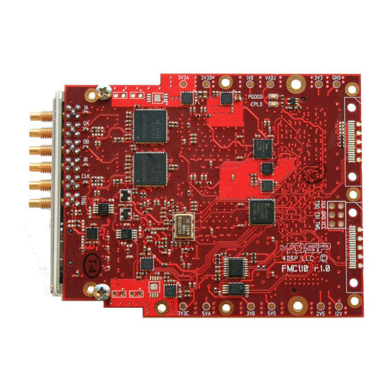
2 General description The FMC204 is a quad-channel D/A FMC. The FMC204 provides four 16-bit D\A channels that enable simultaneous sampling at a maximum rate of 1 Gsps. The sample clock can be supplied externally through a coax connection or by an internal clock source (optionally locked to an external reference). -
Page 6: Installation
The carrier card must support VADJ/VIO_B voltage of +2.5V (LVDS support) for FMC204 revision 1. The carrier card can support VADJ/VIO_B voltage range of 1.65V to 3.3V for FMC204 revision 2, but typically VADJ will be 1.8V or 2.5V for LVDS operation. -
Page 7: Design
4 Design 4.1 Physical specifications 4.1.1 Board Dimensions The FMC204 card complies with the FMC standard known as ANSI/VITA 57.1. The card is a single-width, conduction-cooled mezzanine module (with region 1 and front panel I/O). 4.1.2 Front panel coax inputs There are six coax connectors available from the front panel. -
Page 8: Electrical Specifications
LVCMOS level (V = VADJ). 4.2.1 EEPROM The FMC204 card carries a 2Kbit EEPROM which is accessible from the carrier card through the I C bus. The EEPROM is powered by 3P3VAUX. The standby current is only 0.01µA when SCL and SDA are kept at 3P3VAUX level. - Page 9 UM008 FMC204 User Manual r1.14 # Pairs # Clock pairs # Data pairs LVDS Clock LVDS Trigger LVDS Sync DAC #1 LVDS Clock LVDS Sync LVDS Data DAC #2 LVDS Clock LVDS Sync LVDS Data 2.5V or VADJ Level I/O...
-
Page 10: Main Characteristics
Table 4 : FMC204 daughter card main characteristics 4.4 Analog output channels The FMC204 has four single-ended analog outputs that are AC-coupled from the D/A device. An RF transformer (TC4-1W, 3-800MHz) is used. The analog outputs are designed to drive a 50Ω... -
Page 11: External Trigger/Sync Input
LVDS signal to both D/A converters. 4.7 Clock Tree The FMC204 offers a clock architecture that combines flexibility and high performance. Components have been chosen to minimize jitter and phase noise to reduce degradation of the data conversion performance. The user may use an external or internal sampling clock. -
Page 12: Control
UM008 FMC204 User Manual r1.14 VC(X)O Loop Π-attn Filter 1.0 GHz XTAL CLKSRC_SEL2 100MHz Clock Switch CLKSRC_SEL0 Switch CLKSRC_SEL1 DAC 1 DAC 0 To FMC Figure 4: Clock tree 4.7.1 Control The clock tree contains two RF switches (ADG918) and requires the following control signals (driven from the CPLD): ... - Page 13 UM008 FMC204 User Manual r1.14 Figure 5: MGT interconnect topologies TOP VIEW MICTOR 1 Rx-Tx 0-4 MICTOR 2 Rx-Tx 5-9 FPGA Figure 6: 4DSP CPCI board stack (slot-to-slot) UM008 www.4dsp.com - 13 -...
-
Page 14: Power Supply
N.B. These connectors are not available on the FMC204 revision 2. 4.9 Power supply Power is supplied to the FMC204 card through the FMC connector. The pin current rating is 2.7A, but the overall maximum as specified by the FMC standard is limited according to Table 6. -
Page 15: Synchronizing Multiple Cards
Table 6: FMC standard power specification The power provided by the carrier card can be very noisy. Special care is taken with the power supply generation on the FMC204 card to minimize the effect of power supply noise on clock generation and data conversion. -
Page 16: Controlling The Fmc204
UM008 FMC204 User Manual r1.14 Fs 50% CLOCK Clock generation Fs/4 25% TRIGGER/SYNC FMC204 CLOCK TRIGGER/SYNC FMC204 CLOCK TRIGGER/SYNC FMC204 Figure 7: Synchronizing multiple cards 5 Controlling the FMC204 5.1 Architecture The FMC must be controlled from the carrier hardware through a single SPI communication bus. -
Page 17: Spi Programming
N_RESET on the both DAC5682Z devices is shared. 5.2 SPI Programming The SPI programmable devices on the FMC204 can be accessed as described in their datasheet, but each SPI communication cycle needs to be preceded with a preselection byte. The preselection byte is used by the CPLD to forward the SPI command to the right destination. - Page 18 UM008 FMC204 User Manual r1.14 N_CS SCLK SDIO P0 R/W A6 8-bit pre-selection 8-bit instruction 8-bit register data Figure 9: Write instruction to CPLD registers A1:A0 N_CS SCLK SDIO P0 R/W A6 8-bit pre-selection 8-bit instruction 8-bit register data Figure 10: Read instruction to CPLD registers A1:A0...
-
Page 19: Environment
UM008 FMC204 User Manual r1.14 N_CS SCLK SDIO P0 R/W W1 W0 A12 A11 A10 A9 8-bit pre-selection 16-bit instruction 8-bit register data Figure 14: Read instruction to AD9517 registers A12:A0 6 Environment 6.1 Temperature Operating temperature: ° °... -
Page 20: Cooling
Two different types of cooling are available for the FMC204. 6.3.1 Convection cooling The air flow provided by the fans of the chassis the FMC204 is enclosed in will dissipate the heat generated by the on board components. A minimum airflow of 300 LFM is recommended. -
Page 21: Warranty
UM008 FMC204 User Manual r1.14 9 Warranty Hardware Software/Firmware Basic Warranty 1 Year from Date of Shipment 90 Days from Date of Shipment (included) Extended Warranty 2 Years from Date of Shipment 1 Year from Date of Shipment (optional) UM008 www.4dsp.com... -
Page 22: Appendix Ahpc Pin-Out Fmc204
UM008 FMC204 User Manual r1.14 Appendix A HPC pin-out FMC204 AV57.1 HPC Pin FMC204 Signal AV57.1 HPC Pin FMC204 Signal AV57.1 HPC Pin FMC204 Signal CLK0_M2C_N CLK_TO_FPGA_N HA00_N_CC N.C. HB10_N DAC1_DATA_P<4> CLK0_M2C_P CLK_TO_FPGA_P HA00_P_CC N.C. HB10_P DAC1_DATA_N<4> CLK1_M2C_N TRIGGER_TO_FPGA_N HA01_N_CC N.C. - Page 23 UM008 FMC204 User Manual r1.14 LA18_N_CC N.C. HA22_N N.C. DP4_C2M_N DP_C2M_N<4> LA18_P_CC N.C. HA22_P N.C. DP4_C2M_P DP_C2M_P<4> LA19_N DAC0_DATA_P<10> HA23_N N.C. DP4_M2C_N DP_M2C_N<4> LA19_P DAC0_DATA_N<10> HA23_P N.C. DP4_M2C_P DP_M2C_P<4> LA20_N DAC0_DATA_P<11> HB00_N_CC DAC1_DATA_P<11> DP5_C2M_N DP_C2M_N<5> LA20_P DAC0_DATA_N<11> HB00_P_CC DAC1_DATA_N<11> DP5_C2M_P DP_C2M_P<5>...
- Page 24 FMC204 User Manual r1.13 Table 9: HPC signal description (FMC204) Signal Group Direction I/O Standard Description CLK_TO_FPGA_N D/A 0, D/A 1 Output LVDS Clock to be used as reference clock for generating DAC CLK_TO_FPGA_P clock and data signals. Typically, half of the sample clock frequency.
-
Page 25: Appendix Bcpld Register Map
UM008 FMC204 User Manual r1.14 Appendix B CPLD Register map Bit nr. Bit 7 Bit 6 Bit 5 Bit 4 Bit 3 Bit 2 Bit 1 Bit 0 ‘0’ Name DACR CLKR SYNCSRC CLKSRC Table 10: Register CPLD_REG0 definition Field... - Page 26 Field Description DIRx Direction of Front IO transceiver (x = 0 to 3) ‘0’ Signal x is input (FMC204 is receiver) ‘1’ Signal x is output (FMC204 is transmitter) FANx Power control for FAN header (x = 0 to 3) ‘0‘...
- Page 27 UM008 FMC204 User Manual r1.14 Field Description LED_SEL Writing to this register determines which status signal is indicated by the LED. ‘XXXX1‘ REFMON ‘XXX10‘ ‘XX100‘ STATUS ‘X1000‘ ‘10000‘ Table 17: Register CPLD_REG2 description (write) UM008 www.4dsp.com - 27 -...
Need help?
Do you have a question about the FMC204 and is the answer not in the manual?
Questions and answers