Advertisement
Quick Links
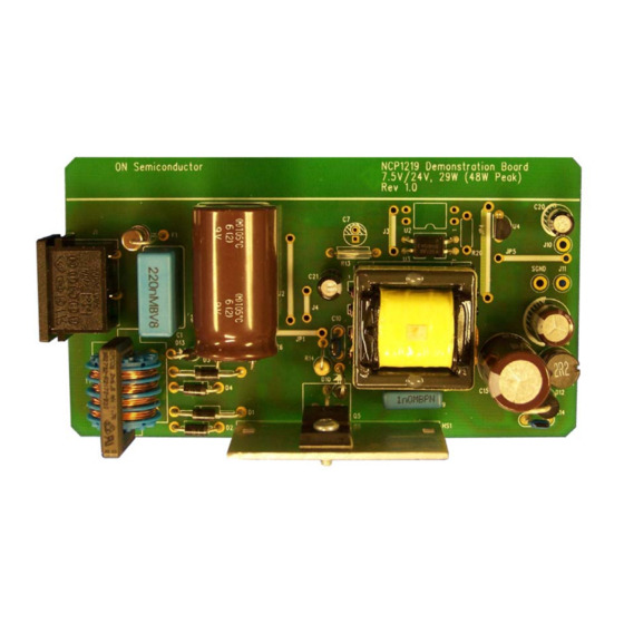
NCP1219PRINTGEVB
NCP1219 48 W Printer
Evaluation Board User's
Manual
Introduction
The NCP1219 is the newest part in the NCP12XX family
of current−mode flyback controllers. The controller features
dynamic self supply (DSS), eliminating the need for
external startup circuitry, contributing to a cost effective,
low parts count flyback controller design. The NCP1219
also includes a user programmable skip cycle threshold,
reducing power dissipation at light loads and in standby
mode. An externally provided latch signal delivered to the
Skip/latch pin allows the realization of protection
functionality.
The 48 W ac adapter evaluation board targets a printer
adapter application with a 24 V output, reconfigurable to
7.25 V in standby mode selectable with an external signal.
The use of DSS mode is demonstrated for low input
voltages, while an auxiliary winding is used for higher input
voltages to maintain standby power below 1 W. The
NCP1219 evaluation board shows latched−mode protection
function through the optional primary and secondary
overvoltage protection circuits.
The evaluation board is designed as an off−line printer
adapter power supply. The adapter operates across universal
inputs, 85 Vac to 265 Vac (47 Hz – 63 Hz). The adapter
supplies a regulated 24 V output. It can deliver a steady state
30 W output with transient capability of 48 W, as defined in
Figure 1.
700 ms
time (ms)
Figure 1. Transient Output Current Specification
The system has a low voltage standby mode enabled by
pulling the MC node low. In standby mode the converter
supplies 70 mA of standby current at 7.25 V while
maintaining input power below 1 W. The system is
self−contained, with the NCP1219 bias being provided by
the bulk voltage through an internal startup circuit. The IC
© Semiconductor Components Industries, LLC, 2012
November, 2012 − Rev. 3
2.0 A
1.25 A
0.92 A
300 ms
1
http://onsemi.com
EVAL BOARD USER'S MANUAL
bias is provided by either DSS for low input voltages, or an
auxiliary winding for higher input voltages. The
specifications are summarized in Table 1.
Table 1. SUMMARY OF EVALUATION BOARD
SPECIFICATIONS
Requirement
Unit
Input Voltage
Vac
Line Frequency
Hz
Output Voltage
Vdc
Output Current
Adc
Output Power
W
Average
h
avg
Efficiency (EPA
Energy Star 2.0
Compliance)
Standby Voltage
Vdc
Standby Power
W
Output Ripple
mV
Voltage
Output Voltage
mV
Under/Overshoot
During Transient
Load Step from
0.92 A to 2.0 A
Design Procedure
The converter design procedure is divided into several
steps:
•
Power Component Selection
•
Loop Stability Analysis and Compensation
•
IC Supply Circuits
•
External Protection Circuits
•
Standby Reconfiguration Circuit
Throughout this application note, the minimum and
maximum input voltages are referred as low and high line,
respectively.
The evaluation board schematic is provided in Figure 2
for reference to component values throughout the design
procedure.
Min
Max
85
265
47
63
23.8
24.2
−
1.25 (2.0 transient
peak)
−
30 (48 transient peak)
83.5
−
7
8
−
1
−
200
−
200
Publication Order Number:
EVBUM2161/D
Advertisement

Related Manuals for ON Semiconductor NCP1219PRINTGEVB


Summary of Contents for ON Semiconductor NCP1219PRINTGEVB
- Page 1 NCP1219PRINTGEVB NCP1219 48 W Printer Evaluation Board User's Manual Introduction http://onsemi.com The NCP1219 is the newest part in the NCP12XX family of current−mode flyback controllers. The controller features EVAL BOARD USER’S MANUAL dynamic self supply (DSS), eliminating the need for external startup circuitry, contributing to a cost effective, low parts count flyback controller design.
- Page 2 NCP1219PRINTGEVB Figure 2. Evaluation Board Schematic http://onsemi.com...
- Page 3 NCP1219PRINTGEVB Transformer voltage supplying the controller. Using a 650 V MOSFET The turns ratio, N, is chosen to minimize the voltage with a derating factor of 0.8 and a clamp voltage ratio, k , of stresses placed on main switch, Q5, and the secondary diode, 1.6 yields a turns ratio of 0.303.
- Page 4 NCP1219PRINTGEVB Primary Switch The power dissipated in the secondary diode, P The main MOSFET switch, Q5, is selected to operate at approximated by Equation 13, where V is the forward a junction temperature of 120°C at an ambient temperature voltage of the selected diode, and I is the nominal output of 85°C.
- Page 5 NCP1219PRINTGEVB Auxiliary Supply Regulator The HV pin of the NCP1219 can be tied directly to the (eq. 19) bulk storage capacitor and used to supply the IC in the bulk absence of an auxiliary winding, for instance, during the This implies that, as the input voltage drops, the auxiliary startup of the adapter.
- Page 6 NCP1219PRINTGEVB winding. Care must be taken not to exceed the thermal where I is the specified minimum startup current start(min) capability of the IC. The power dissipated during DSS mode provided to the V pin. I = 5 mA and assuming start(min) is approximated by Equation 20.
- Page 7 NCP1219PRINTGEVB The average HV pin voltage, V , is AVG(half−wave) calculated using Equation 26. Peak (eq. 26) AVG(half*wave) In comparison, using the example from option 2 (full−time DSS mode with the HV pin connected to V bullk power dissipation, P , of 270 mW, and a junction temperature of 107°C is achieved.
- Page 8 The gain and pole and zero placement of the feedback network are selected to achieve the desired crossover frequency and phase margin. ON Semiconductor provides the excel based design tool ”FLYBACK AUTO”. It provides an automated method of compensating the feedback loop of an isolated flyback converter using the TL431 and an optocoupler.
- Page 9 NCP1219PRINTGEVB Figure 13. Optocoupler Frequency Analysis Test Circuit From Figure 14, the crossover frequency of the SFH615A−3 is measured at 4.7 kHz. From the dc bias of the optocoupler, the current transfer ratio, CTR is measured as 41%. These values are used in the optocoupler page of the compensation tool.
- Page 10 NCP1219PRINTGEVB 1 0 0 -2 0 -6 0 -1 0 -1 0 0 −17 dB -2 0 -1 4 0 -3 0 -1 8 0 -4 0 -2 2 0 Mag (dB) -5 0 -2 6 0 Phase (°) -6 0...
-
Page 11: Frequency (Hz)
NCP1219PRINTGEVB Figure 19 compares the measured results to the frequency (eq. 33) response produced by the “FLYBACK AUTO” tool. There 2 @ p @ L1 @ C16 is good agreement for frequencies at or below the crossover where L1 is the output inductor and C16 is the output filter frequency. - Page 12 NCP1219PRINTGEVB Under light load conditions, the controller enters skip For the evaluation board design, the NCP1219 default mode. As seen in Figure 21, when V (C3) decreases to less skip threshold is used to reduce component count. Selecting than V (C1) the drive pulses stop (C4).
- Page 13 NCP1219PRINTGEVB This effect is called “Over power” because it increases the 2 @ P power at which the overcurrent protection disables the (eq. 35) peak controller. Specifically, for a DCM flyback system, the total Using the measured output power at high line, the power delivered to the output including the propagation calculated peak current of 2.63 A causes a voltage on the...
-
Page 14: Soft Start
NCP1219PRINTGEVB Overvoltage Protection options included on this evaluation board. For example, the Overvoltage protection (OVP) is implemented on this latch pin may be used to implement temperature shutdown evaluation board using one of two options; primary side externally using an NTC element driving the base of a overvoltage protection or secondary side overvoltage bipolar transistor, Q1, as shown in Figure 27. - Page 15 NCP1219PRINTGEVB Figure 29. Startup Waveforms Showing Soft−Start Behavior; C1 = V , C4 = V Board Layout 3. Use a single ground connection. The evaluation board is built using a double sided FR4 4. Keep sensitive nodes away from noisy nodes such board.
- Page 16 NCP1219PRINTGEVB Figure 30. Layer 1 (Top) Figure 31. Layer 2 (Bottom) http://onsemi.com...
- Page 17 NCP1219PRINTGEVB Figure 31 shows the bottom layer of the PC board, Design Validation The top and bottom view of the board are shown in including the silkscreen, copper, and soldermask. Figures 32 and 33, respectively. The layout files may be available. Please contact your sales representative for availability.
- Page 18 NCP1219PRINTGEVB The bill of materials that accompanies the evaluation board circuit schematic of Figure 2 is listed in Table 2. Table 2. BILL OF MATERIALS Substi- Desig- Toler- Manufacturer Part tution Lead nator Description Value ance Footprint Manufacturer Number Allowed...
- Page 19 NCP1219PRINTGEVB Table 2. BILL OF MATERIALS Substi- Desig- Toler- Manufacturer Part tution Lead nator Description Value ance Footprint Manufacturer Number Allowed Free Header, 1 Row of 0.156 Molex 26-64-4030 Electrical Connection on Top Layer of PCB jumper wire 22 AWG...
- Page 20 NCP1219PRINTGEVB Table 2. BILL OF MATERIALS Substi- Desig- Toler- Manufacturer Part tution Lead nator Description Value ance Footprint Manufacturer Number Allowed Free R41, Resistor, SMD 1.8 kW 0.01 SM/1206 Vishay CRCW12061801FN R51, Resistor, SMD 1.69 W 0.01 SM/1206 Vishay CRCW12061R69FN...
- Page 21 NCP1219PRINTGEVB Input Voltage (Vac) Figure 35. Average Efficiency vs. Line Voltage The standby input power requirement is less than 1 W A portion of the standby input power is due to the startup over the range of input voltage. Figure 36 shows the standby circuit.
- Page 22 NCP1219PRINTGEVB The output voltage ripple is measured at 16 mV at high switching frequency appears as expected. The output filter line and full load. It is significantly less than the 50 mV eliminates the ripple associated with the switching target. The output voltage ripple waveform at high line and frequency, leaving only low amplitude spikes of noise that full load is shown in Figure 37.
- Page 23 NCP1219PRINTGEVB The dynamic response of the converter at 24 V is as 150 mV, and recovery occurs in less than 5 ms. Response evaluated stepping the load current from 0.92 A to 2.0 A and to the transient load condition confirms the results of the from 2.0 A to 0.92 A.
- Page 24 NCP1219PRINTGEVB Thermal Performance of the board during a continuous load step as described in This evaluation board is designed to operate with out Figure 1. Images include top and bottom layers at low and forced airflow as in an external printer power supply. The high line.
- Page 25 NCP1219PRINTGEVB Figure 42. Thermal Image of the Top of the Board at High Line During a Continuous Load Step Condition Figure 43. Thermal Image of the Bottom of the Board at High Line During a Continuous Load Step Condition http://onsemi.com...
- Page 26 NCP1219PRINTGEVB Most of the losses on the board are on the main switch, achieved using a forward auxiliary winding with DSS transformer, secondary rectifier (D12) and secondary operating at low line conditions only. The converter snubber resistor (R18). The main switch losses are complies with Energy Star 2.0 EPS requirements.
- Page 27 NCP1219PRINTGEVB TEST PROCEDURE FOR THE NCP1219PRINTGEVB EVALUATION BOARD Required Equipment 60minutes + (W (*Equivalent test equipment may be submitted.) 5minutes 1hour • Record the results in Table 5. Verify it is within the *Chroma 61604 AC Power Source • limits of Table 4.
- Page 28 NCP1219PRINTGEVB Figure 44. Test Setup Table 3. NORMAL OPERATING CONDITIONS Table 4. DESIRED RESULTS Input Voltage Line Frequency Input Voltage (Vac) (Hz) Load Current (A) 70 mA 7 V < V < OUT(standby) 0.01 70 mA < 1 W 0.3125 (25%)
- Page 29 PUBLICATION ORDERING INFORMATION LITERATURE FULFILLMENT: N. American Technical Support: 800−282−9855 Toll Free ON Semiconductor Website: www.onsemi.com Literature Distribution Center for ON Semiconductor USA/Canada Order Literature: http://www.onsemi.com/orderlit P.O. Box 5163, Denver, Colorado 80217 USA Europe, Middle East and Africa Technical Support: Phone: 303−675−2175 or 800−344−3860 Toll Free USA/Canada...
Need help?
Do you have a question about the NCP1219PRINTGEVB and is the answer not in the manual?
Questions and answers