Sign In
Upload
Manuals
Brands
Nvidia Manuals
Computer Hardware
Jetson Orin NX
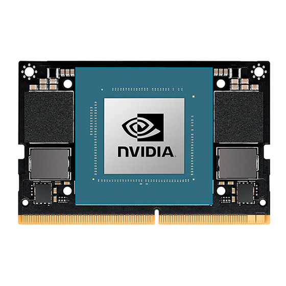
Nvidia Jetson Orin NX Manuals
Manuals and User Guides for Nvidia Jetson Orin NX. We have
1
Nvidia Jetson Orin NX manual available for free PDF download: Design Manual
Nvidia Jetson Orin NX Design Manual (90 pages)
Brand:
Nvidia
| Category:
Computer Hardware
| Size: 2.59 MB
Table of Contents
Table of Contents
3
Chapter 1. Introduction
9
References
9
Attachments
9
Abbreviations and Definitions
10
Table 1-1. Abbreviations and Definitions
10
Chapter 2. Jetson Orin NX
11
Table 2-1. Jetson Orin NX Interfaces
11
Figure 2-1. Jetson Orin NX Block Diagram
12
Table 2-2. Jetson Orin NX Connector 260-Pin SO-DIMM Pinout Matrix
12
Chapter 3. Jetson Orin NX Boot Considerations
16
QSPI Boot
16
USB Recovery Mode
16
Chapter 4. Developer Kit Feature Considerations
17
Button Power MCU
17
USB Superspeed Hub
18
Power over Ethernet
18
TI TXB0108 Level Shifters
18
Features Not to be Implemented
18
Chapter 5. Modular Connector
19
Module Connector Details
19
Module to Mounting Hardware
19
Module Installation and Removal
20
Figure 5-1. Jetson Orin NX Module Installed in SODIMM Connector
20
Figure 5-2. Module to Connector Assembly Diagram
20
Chapter 6. Power
21
Table 6-1. Jetson Orin NX Power and System Pin Description
21
Power Supply and Sequencing
22
Figure 6-1. System Power and Control Block Diagram
24
Figure 6-2. System Power and Control Block Diagram
24
Figure 6-3. Power up Sequence no Power Button - Auto Power on
25
Figure 6-4. Power up Sequence with Power Button
25
Figure 6-5. Power down Initiated by SHUTDOWN_REQ* Assertion
26
Figure 6-6. Power down Sudden Power Loss
26
Chapter 7. USB and Pcie
27
Table 7-1. Jetson Orin NX USB 2.0 Pin Description
27
Table 7-2. Jetson Orin NX USB 3.2 and Pcie Pin Description
28
Table 7-3. USB SS and Pcie Lane Mapping
30
Usb
31
Figure 7-1. USB Micro B USB Device and Recovery Connection Example
31
Figure 7-2. USB SS Type a Host Only Connection Example
31
USB 2.0 Design Guidelines
32
USB 3.2 Design Guidelines
32
Table 7-4. USB 2.0 Interface Signal Routing Requirements
32
Table 7-5. USB 3.2 Interface Signal Routing Requirements
32
Figure 7-3. IL/NEXT Plot
35
Figure 7-4. TDR Plot
35
Figure 7-5. Via Topology
35
Figure 7-6. Component Order
35
Common USB Routing Guidelines
36
Figure 7-7. Component Placement
36
Figure 7-8. ESD Layout Recommendations
36
Table 7-6. Orin USB 2.0 Signal Connections
36
Table 7-7. Miscellaneous USB 2.0 Signal Connections
36
Pcie
37
Table 7-8. Orin USB 3.2 Signal Connections
37
Figure 7-9. Pcie Root Port Connections Example
38
Figure 7-10. Pcie Endpoint Connections Example
39
Pcie Design Guidelines
40
Table 7-9. Pcie Interface Signal Routing Requirements up to Gen4
40
Figure 7-11. Zig-Zag Routing Example
41
Figure 7-12. Insertion Loss S-Parameter Plot SDD21
42
Figure 7-13. Insertion Loss S-Parameter Plot SDD11
42
Figure 7-14. AC Cap Voiding
42
Figure 7-15. Connector Voiding
42
Table 7-10. Pcie Signal Connections
43
Chapter 8. Gigabit Ethernet
45
Figure 8-1. Jetson Orin NX Ethernet Connections
45
Table 8-1. Jetson Orin NX Gigabit Ethernet Pin Descriptions
45
Figure 8-2. Gigabit Ethernet Magnetics and RJ45 Connections
46
Table 8-2. Ethernet MDI Interface Signal Routing Requirements
46
Table 8-3. Ethernet Signal Connections
46
Chapter 9. Display
47
Table 9-1. Jetson Orin NX Edp, DP, and HDMI Pin Descriptions
47
Edp and DP
48
Figure 9-1. DP and Edp Connection Example
48
Table 9-2. DP and HDMI Pin Mapping
48
Edp and DP Routing Guidelines
49
Figure 9-2. DP++ Connection Example
49
Figure 9-3. Edp and DP Differential Main Link Topology
49
Table 9-3. Edp and DP Main Link Signal Requirements Including DP_AUX
50
Figure 9-4. S-Parameter up to HBR2
52
Figure 9-5. S-Parameter up to HBR3
52
Figure 9-6. Via Topology #1
53
Figure 9-7. Via Topology #2
53
Table 9-4. Edp and DP Signal Connections
53
Hdmi
54
Figure 9-8. HDMI Connection Example
54
Figure 9-9. HDMI CLK and Data Topology
55
Table 9-5. HDMI Interface Signal Routing Requirements
55
Figure 9-10. IL/FEXT Plot
58
Figure 9-11. TDR Plot
58
Figure 9-12. HDMI Via Topology
58
Figure 9-13. Connector Pin Via
59
Figure 9-14. Via no Breakout
59
Figure 9-15. Via Breakout on same Layer as Main Trunk
59
Figure 9-16. Add on Components - Top
59
Figure 9-17. Add on Components - Bottom
59
Figure 9-18. AC Cap Void
60
Figure 9-19. RPD, Choke, FET Placement
60
Figure 9-20. ESD Footprint
60
Figure 9-21. ESD Void
60
Figure 9-22. SMT Pad Trace Entering
60
Figure 9-23. SMT Pad Trace between
60
Figure 9-24. Connector Voiding
61
Table 9-6. HDMI Signal Connections
61
Chapter 10. MIPI CSI Video Input
62
Table 10-1. Jetson Orin NX CSI Pin Descriptions
62
Figure 10-1. CSI Connection Options
63
Table 10-2. Jetson Orin NX Camera Miscellaneous Pin Descriptions
63
CSI Design Guidelines
64
Figure 10-2. Available Camera Control Pins
64
Table 10-3. CSI Configurations
64
Table 10-4. MIPI CSI Interface Signal Routing Requirements
64
Table 10-5. MIPI CSI Signal Connections
65
Table 10-6. Miscellaneous Camera Connections
65
Chapter 11. Audio
66
Table 11-1. Jetson Orin NX Audio Pin Descriptions
66
Figure 11-1. Audio Connection Example
67
Table 11-2. I2S Interface Signal Routing Requirements
67
Table 11-3. Audio Signal Connection
68
Chapter 12. Miscellaneous Interfaces
69
I2C
69
Table 12-1. Jetson Orin NX I2C Pin Descriptions
69
I2C Design Guidelines
70
Figure 12-1. I2C Connections
70
Table 12-2. I2C Interface Signal Routing Requirements
70
Spi
71
Table 12-3. I2C Signal Connections
71
Table 12-4. Jetson Orin NX SPI Pin Descriptions
71
Figure 12-2. SPI Connections
72
Figure 12-3. Basic SPI Initiator and Target Connections
72
SPI Design Guidelines
73
Figure 12-4. SPI Topologies
73
Table 12-5. SPI Interface Signal Routing Requirements
73
Table 12-6. SPI Signal Connections
73
Uart
74
Figure 12-5. Jetson Orin NX UART Connections
74
Table 12-7. Jetson Orin NX UART Pin Descriptions
74
Can
75
Figure 12-6. Jetson Orin NX CAN Connections
75
Table 12-8. UART Signal Connections
75
Table 12-9. Jetson Orin NX CAN Pin Descriptions
75
Table 12-10. CAN Interface Signal Routing Requirements
75
Fan
76
Figure 12-7. Jetson Orin NX Fan Connections
76
Table 12-11. CAN Signal Connections
76
Table 12-12. Jetson Orin NX Fan Pin Descriptions
76
Debug
77
Figure 12-8. Debug UART Connections
77
Table 12-13. Jetson Orin NX Debug UART Pin Descriptions
77
Table 12-14. Debug UART Connections
77
Chapter 13. PADS
78
Internal Pull-Ups for Dual Voltage Block Pins Power at 1.8V
78
Schmitt Trigger Usage
78
Pins Pulled or Driven High During Power-On
79
Table 13-1. Pins Pulled or Driven High by Orin Prior to SYS_RESET* Inactive
79
Table 13-2. Pins with External Pull-Ups to Supply on before SYS_RESET* Inactive
79
Chapter 14. Unused Interface Terminations
80
Unused Multi-Purpose Standard CMOS Pad Interfaces
80
Unused Dedicated Special Purpose Pad Interfaces
80
Table 14-1. Unused MPIO Pins and Pin Group
80
Chapter 15. Design and Bring-Up Checklists
81
Chapter 16. Jetson Orin NX Pin Descriptions
82
Chapter 17. General Routing Guidelines
83
Signal Naming Convention
83
Table 17-1. Signal Type Codes
83
Routing Guidelines Format
84
Signal Routing Conventions
84
Routing Guidelines
84
General PCB Routing Guidelines
85
Figure 17-1. General PCB Routing Guidelines
85
Common High-Speed Interface Requirements
86
Figure 17-2. Common Mode Choke
86
Table 17-2. Common High-Speed Interface Requirements
86
Test Points for High-Speed Interfaces
87
Figure 17-3. Serpentine
87
Chapter 18. USB SS and Wireless Coexistence
88
Mitigation Techniques
88
Advertisement
Advertisement
Related Products
Nvidia JETSON DEVELOPER KIT
Nvidia Jetson AGX Orin Series
Nvidia Jetson AGX Xavier Series
Nvidia JETSON AGX XAVIER
Nvidia JETSON NANO
Nvidia JETSON XAVIER NX
Nvidia Jetson Nano Developer Kit
Nvidia Jetson Orin NX Series
Nvidia Jetson Orin Nano Series
Nvidia 6200
Nvidia Categories
Video Card
Computer Hardware
Motherboard
Microcontrollers
Adapter
More Nvidia Manuals
Login
Sign In
OR
Sign in with Facebook
Sign in with Google
Upload manual
Upload from disk
Upload from URL