Sign In
Upload
Manuals
Brands
Nvidia Manuals
Microcontrollers
JETSON NANO
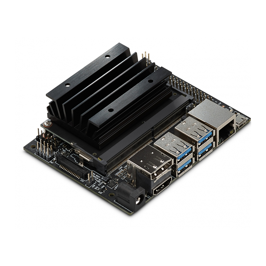
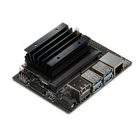
Nvidia JETSON NANO Manuals
Manuals and User Guides for Nvidia JETSON NANO. We have
4
Nvidia JETSON NANO manuals available for free PDF download: Product Design Manual, Manual, Support Manual, User Manual
Nvidia JETSON NANO Product Design Manual (84 pages)
Brand:
Nvidia
| Category:
Microcontrollers
| Size: 2.04 MB
Table of Contents
Table of Contents
3
Chapter 1. Introduction
9
References
9
Abbreviations and Definitions
10
Table 1-1. Abbreviations and Definitions
10
Chapter 2. Jetson Nano
12
Table 2-1. Jetson Nano Interfaces
12
Figure 2-1. Jetson Nano Block Diagram
13
Table 2-2. Jetson Nano Connector Pinout Matrix
13
Chapter 3. Developer Kit Feature Considerations
15
USB Superspeed Hub
15
Power over Ethernet (Poe)
15
TI TXB0108 Level Shifters
16
Features Not to be Implemented
16
Chapter 4. Modular Connector
17
Module Connector Details
17
Module to Mounting Hardware
17
Module Installation and Removal
18
Figure 4-1. Jetson Nano Module Installed in SODIMM Connector
18
Figure 4-2. Module to Connector Assembly Diagram
18
Chapter 5. Power
19
Table 5-1. Jetson Nano Power and System Pin Descriptions
19
Power Supply and Sequencing
20
Figure 5-1. Jetson Nano Power and Control Block Diagram
20
Figure 5-2. System Power and Control Block Diagram
21
Figure 5-3. Power up Sequence
21
Figure 5-4. Power down - Initiated by SHUTDOWN_REQ* Assertion)
21
Figure 5-5. Power down - Sudden Power Loss
22
Chapter 6. USB and PCI Express
23
Table 6-1. Jetson Nano USB 2.0 Pin Descriptions
23
Table 6-2. Jetson Nano USB 3.0 and Pcie Pin Descriptions
23
Table 6-3. Jetson Nano USB 3.0 and Pcie Lane Mapping Configurations
24
Usb
25
Figure 6-1. USB Connection Example
25
Table 6-4. USB 2.0 Interface Signal Routing Requirements
26
Table 6-5. USB 3.0 Interface Signal Routing Requirements
26
USB 2.0 Design Guidelines
26
USB 3.0 Design Guidelines
26
Figure 6-2. IL/NEXT Plot
28
Figure 6-3. Trace Spacing for TX/RX Non-Interleaving
28
Figure 6-4. Via Structures
28
Common USB Routing Guidelines
29
Figure 6-5. ESD Layout Recommendations
29
Figure 6-6. Component Order
29
Table 6-6. Tegra USB 2.0 Signal Connections
29
Pcie
30
Table 6-7. Miscellaneous USB 2.0 Signal Connections
30
Table 6-8. Tegra USB 3.0 Signal Connections
30
Figure 6-7. Example Pcie Connections
31
Pcie Design Guidelines
31
Table 6-9. Pcie Interface Signal Routing Requirements
31
Figure 6-8. AC Cap Voiding
33
Table 6-10. Pcie Signal Connections
33
Figure 6-9. Jetson Nano Ethernet Connections
34
Gigabit Ethernet
34
Table 6-11. Jetson Nano Gigabit Ethernet Pin Description
34
Figure 6-10. Gigabit Ethernet Magnetics and RJ45 Connections
35
Table 6-12. Ethernet MDI Interface Signal Routing Requirements
35
Table 6-13. Ethernet Signal Connections
35
Chapter 7. Display
36
Mipi Dsi
36
Table 7-1. Jetson Nano Display General Pin Description
36
Figure 7-1. DSI 1 X 2 Lane Connection Example
37
Table 7-2. Jetson Nano DSI Pin Description
37
MIPI DSI and CSI Connection Guidelines
38
MIPI DSI and CSI Design Guidelines
38
Table 7-3. MIPI DSI and CSI Interface Signal Routing Requirements
38
Table 7-4. MIPI DSI Signal Connections
38
Edp and DP
39
Table 7-5. Jetson Nano Edp and DP Pin Description
39
Figure 7-2. Dp/Edp Connection Example on DP0 Pins
40
Edp Routing Guidelines
41
Figure 7-3. Edp Differential Main Link Topology
41
Table 7-6. Edp and DP Main Link Signal Routing Requirements Including DP_AUX
41
Figure 7-4. S-Parameter
43
Figure 7-5. Via Topology #1
43
Figure 7-6. Via Topology #2
43
Table 7-7. Edp Signal Connections
43
HDMI and DP
44
Table 7-8. Jetson Nano HDMI and DP Pin Description
44
Table 7-9. DP and HDMI Pin Mapping
44
Figure 7-7. HDMI Connection Example
45
Hdmi
45
Figure 7-8. HDMI Clk and Data Topology
46
Table 7-10. HDMI Interface Signal Routing Requirements
46
Figure 7-10. TDR Plot
49
Figure 7-11. HDMI Via Topology
49
Figure 7-12. Add-On Components - Top
49
Figure 7-9. IL and FEXT Plot
49
Figure 7-13. Add-On Components - Bottom
50
Figure 7-14. AC Cap Void
50
Figure 7-15. RPD, Choke, FET Placement
50
Figure 7-16. ESD Footprint
50
Figure 7-17. ESD Void
50
Figure 7-18. SMT Pad Trace Entering
51
Figure 7-19. SMT Pad Trace between
51
Figure 7-20. Connector Voiding
51
Table 7-11. HDMI Signal Connections
51
DP on DP1 Pins
52
Figure 7-21. DP Connection Example
52
DP Interface Signal Routing Requirements
53
Table 7-12. DP Signal Connections
53
Chapter 8. MIPI CSI Video Input
54
Table 8-1. Jetson Nano CSI Pin Description
54
Table 8-2. Jetson Nano Camera Miscellaneous Pin Description
55
Figure 8-1. 4 Lane CSI Camera Connection Example
56
Table 8-3. CSI Configuration
56
Figure 8-2. Available Cameral Control Pins
57
Figure 8-3. CSI Connection Options
57
CSI Design Guidelines
58
Table 8-4. MIPI CSI Signal Connections
58
Table 8-5. Miscellaneous Camera Connections
58
Chapter 9. SD Card and SDIO
59
Table 9-1. Jetson Nano SDIO Pin Description
59
Figure 9-1. SD Card Connection Example
60
Table 9-2. SD Card and SDIO Interface Signal Routing Requirements
60
Table 9-3. SD Card and SDIO Signal Connections
61
Chapter 10. Audio
62
Table 10-1. Jetson Nano Audio Pin Description
62
Figure 10-1. Audio Codec Connection Example
63
Table 10-2. Interface Signal Routing Requirements
64
Table 10-3. Audio Signal Connections
64
Chapter 11. Miscellaneous Interfaces
65
Table 11-1. Jetson Nano I2C Pin Description
65
I2C Design Guidelines
66
Figure 11-1. I2C Connections
66
Spi
67
Table 11-2. I2C Interface Signal Routing Requirements
67
Table 11-3. I2C Signal Connections
67
Table 11-4. Jetson Nano SPI Pin Description
67
Figure 11-2. SPI Connections
68
Figure 11-3. Basic SPI Master and Slave Connections
68
Figure 11-4. SPI Topologies
69
SPI Design Guidelines
69
Table 11-5. SPI Interface Signal Routing Requirements
69
Uart
70
Figure 11-5. Jetson Nano UART Connections
70
Table 11-6. Jetson Nano UART Pin Description
70
Fan
71
Table 11-7. UART Signal Connections
71
Table 11-8. Jetson Nano Fan Pin Description
71
Debug
72
Figure 11-6. Jetson Nano Fan Connections
72
Table 11-9. Jetson Nano JTAG and Debug UART Description
72
Figure 11-7. JTAG and Debug UART Connections
73
Figure 11-8. JTAG Test Point Detail
73
Jtag
73
Debug UART
74
Table 11-10. JTAG Connections
74
Table 11-11. Debug UART Connections
74
Chapter 12. PADS
75
Internal Pull-Ups for Dual-Voltage Block Pins Powered at 1.8V
75
Schmitt Trigger Usage
75
Pins Pulled and Driven High During Power-ON
76
Table 12-1. Pins Pulled and Driven High by Tegra Prior to SYS_RESET* Inactive
76
Chapter 13. Unused Interface Terminations
77
Unused Multi-Purpose Standard CMPS Pad Interfaces
77
Table 13-1. Unused MPIO Pins and Pin Groups
77
Chapter 14. Jetson Nano Pin Descriptions and Design Checklist
78
Chapter 15. General Routing Guidelines
79
Signal Name Conventions
79
Table 15-1. Signal Type Codes
79
Routing Guideline Format
80
Signal Routing Conventions
80
General Routing Guidelines
80
General PCB Routing Guidelines
81
Figure 15-1. GSSG Stack-Up
81
Common High-Speed Interface Requirements
82
Table 15-2. Common High-Speed Interface Requirements
82
Figure 15-2. Common Mode Choke
83
Figure 15-3. Serpentine
83
Advertisement
Nvidia JETSON NANO Manual (39 pages)
Platform Adaptation and Bring-Up
Brand:
Nvidia
| Category:
Microcontrollers
| Size: 0.62 MB
Table of Contents
Table of Contents
3
Board Configuration
5
Board Naming
6
Placeholders in the Porting Instructions
6
Pinmux Changes
7
Root Filesystem Configuration
7
Exporting Pinmux for U-Boot
8
Accessing Gpios Via "Gpio" Device Labels
10
Exporting Pinmux for the L4T Linux Kernel
10
Porting U-Boot
10
Porting the Linux Kernel
11
Porting USB
13
USB Structure
13
UPHY Lane Assignment
13
Table 1. Available Outputs for the P3449 Carrier Board
14
Table 2. UPHY Lane Assignment Use Cases
14
Required Device Tree Changes
16
For a Host-Only Port
16
For an OTG (On-The-Go) Port
20
Figure 1. an OTG Port Connector
20
Figure 2. Example of an OTG Port's General Design
22
Table 3. GPIO States and Corresponding Output Cable States
23
Fan Speed Control Mapping Table
29
Boot Time Reduction
30
Root Filesystem
30
Kernel
31
Other Considerations When Porting
30
Hardware Bring-Up Checklist
31
Before Power-On
32
Initial Power-On
32
Initial Software Flashing
32
Power
33
Power Optimization
33
Usb 2.0 Phy
33
Usb 3.0
34
Hdmi
34
Audio
34
Uart
34
SD Card (SDMMC1)
35
Fan
35
Sensors I2C: General
35
Sensors I2C: Touch Screen (Optional)
35
PEX (Optional)
35
Embedded Display(S) (Optional)
36
Imager(S) (Optional)
36
Software Bring-Up Checklist
37
Preparation
37
Bring-Up Hardware Validation
37
U-Boot Port and Boot Validation
37
Kernel and Peripherals, Port and Validation
37
System Power and Clocks
38
Nvidia JETSON NANO User Manual (24 pages)
Brand:
Nvidia
| Category:
Microcontrollers
| Size: 1.24 MB
Table of Contents
Note
2
Table of Contents
3
Developer Kit Setup and Hardware
4
Developer Kit Setup
4
Included in the Box
5
Developer Kit Interfaces
5
Interface Details
6
Power Guide
7
Jetpack
9
Summary of Jetpack Components
9
How to Install Jetpack
11
Working with L4T
12
Compliance Information
13
United States
13
Canada
14
Innovation, Science and Economic Development Canada (ISED)
14
European Union
15
Australia and New Zealand
15
Japan
15
South Korea
18
Russia/Kazakhstan/Belarus
20
Taiwan
20
China
21
India
22
Advertisement
Nvidia JETSON NANO Support Manual (31 pages)
DEVELOPER KIT
Brand:
Nvidia
| Category:
Computer Hardware
| Size: 1.03 MB
Table of Contents
Safety Information
4
Informations de Sécurité
6
Informazioni Per la Sicurezza
8
Wichtige Sicherheitshinweise
10
Información sobre Seguridad
12
Информация По Технике Безопасности
14
Informacje Dotyczące Bezpieczeństwa
16
Advertisement
Related Products
Nvidia JETSON AGX XAVIER
Nvidia JETSON XAVIER NX
Nvidia Jetson Nano Developer Kit
Nvidia Jetson Orin NX
Nvidia JETSON DEVELOPER KIT
Nvidia Jetson AGX Orin Series
Nvidia Jetson AGX Xavier Series
Nvidia Jetson Orin NX Series
Nvidia Jetson Orin Nano Series
Nvidia Clara AGX
Nvidia Categories
Video Card
Computer Hardware
Motherboard
Microcontrollers
Adapter
More Nvidia Manuals
Login
Sign In
OR
Sign in with Facebook
Sign in with Google
Upload manual
Upload from disk
Upload from URL