Table of Contents
Advertisement
Quick Links
Errata
Title & Document Type:
8559A Spectrum Analyzer Operation and Service Manual
Manual Part Number:
08559-90013
January 1984
Revision Date:
HP References in this Manual
This manual may contain references to HP or Hewlett-Packard. Please note that Hewlett-
Packard's former test and measurement, semiconductor products and chemical analysis
businesses are now part of Agilent Technologies. We have made no changes to this
manual copy. The HP XXXX referred to in this document is now the Agilent XXXX.
For example, model number HP8648A is now model number Agilent 8648A.
About this Manual
We've added this manual to the Agilent website in an effort to help you support your
product. This manual provides the best information we could find. It may be incomplete
or contain dated information, and the scan quality may not be ideal. If we find a better
copy in the future, we will add it to the Agilent website.
Support for Your Product
Agilent no longer sells or supports this product. You will find any other available
product information on the Agilent Test & Measurement website:
www.tm.agilent.com
Search for the model number of this product, and the resulting product page will guide
you to any available information. Our service centers may be able to perform calibration
if no repair parts are needed, but no other support from Agilent is available.
Advertisement
Chapters
Table of Contents
Troubleshooting

Related Manuals for HP 8559A


Summary of Contents for HP 8559A
- Page 1 Agilent Technologies. We have made no changes to this manual copy. The HP XXXX referred to in this document is now the Agilent XXXX. For example, model number HP8648A is now model number Agilent 8648A.
- Page 2 OPERATION AND SERVICE A N U A L SPECTRUM ANALYZER...
- Page 3 HEWLETT PACKARD OPERATION AND SERVICE MANUAL 8559A SPECTRUM ANALYZER 21 GHz SERIAL NUMBERS This manual applies directly to instruments with serial numbers prefixed 2347A. With modifications described in Section VII, this manual also applies to instruments with serial num- ber prefixes 1909A through 2320A.
- Page 4 Page ....3-29. Display Adjustments - HP 853A GENERAL INFORMATION ......
-
Page 5: Table Of Contents
7- 1 Contact Cleaning ....The HP 8559A Spectrum Analyzer 7-1. Introduction .... - Page 6 GENERAL INFORMATION MODEL 8559A SAFETY SYMBOLS The following safety symbols are used throughout this manual and in the instrument. Familiarize yourself with each of the symbols and its meaning before operating this instrument. Instruction manual symbol. The instrument will be marked with this symbol when it is necessary for the user to refer to the instruction manual in order to protect the instrument against damage.
- Page 7 GENERAL INFORMATION MODEL 8559A SPECTRUM ANALYZER ADAPTER SIDE STOP K I T OVERLAY K I T 1250-0780 08558-601 31 5060-03 1 9 FIGURE 1-1. HP MODEL8559A SPECTRUM ANALYZER AND ACCESSORIES SUPPLIED...
- Page 8 1-3. DESCRIPTION and/or assemblies for the instrument. SECTION VII, MANUAL BACKDATING 1-4. The H P 8559A displays the amplitude and fre- CHANGES; contains backdating information quency of each component of an input signal on a to make this manual compatible with earlier CRT.
- Page 9 GENERAL INFORMATION MODEL 8559A 1-1 1. SAFETY CONSIDERATIONS Manual Updating supplement. This supplement con- tains change information that explains how to adapt the manual to the newer instrument. 1-12. Before operating this instrument, you should familiarize yourself with the safety markings on the 1-18.
- Page 10 MODEL 8559A GENERAL INFORMATION TABLE HP MODEL8569A SPECIFICATIONS 1-1. SPECIFICATIONS Frequency Readout Resolution FREQUENCY SPECIFICATIONS 1 MHz FREQUENCY RANGE Frequency Span Accuracy 5% of displayed frequency separation 10 MHz to 21 GHz, covered in six pushbutton- selectable ranges: SPECTRAL RESOLUTION AND STABILITY...
- Page 11 GENERAL INFORMATION MODEL 8559A TABLE 1-1. HP MODEL 8559A SPECIFICATIONS (2 OF 4) Maximum lnput (without damage) Levels Calibrator Output Total Power: 10 dBm 0.3 dB (into +20 dBm (O.lW, 2.2 Vrms) with 0 dB input 35 MHz attenuation +30 dBm (lW, 7.1 Vrms) with...
- Page 12 GENERAL INFORMATION MODEL 8559A TABLE 1-1. HP MODEL 8559A SPECIFICATIONS (3 OF 4) Display Fidelity Conducted and radiated interference is in com- CRT linearity and log or linear fidelity affect pliance with MIL-STD 461A, Methods CEO3 amplitude accuracy at levels other than Refer- and RE02, CISPR Publication 11 (1975) and ence Level.
- Page 13 GENERAL INFORMATION MODEL 6559A TABLE 1.1. HP MODEL8559A SPECIFICATIONS (4 OF 4) DIMENSIONS HP Model 182T Display: HP Model 8559A Spectrum Analyzer: 201.6 Note: Dimensions in millimeten and (inches). 34.9 498.5 (19 5 (17 13116)-4 HP Model 181T Display: HP Model 853A Display:...
- Page 14 MODEL 8559A GENERAL INFORMATION TABLE 1-2. MODEL 8559N180-SERIES SUPPLEMENTAL CHARACTERISTICS (1 OF 3) SUPPLEMENTAL CHARACTERISTICS Values in this table are not specifications. They are typical characteristics NOTE: included for user information. AMPLITUDE CHARACTERISTICS FREQUENCY CHARACTERISTICS AMPLITUDE RANGE AND ACCURACY FREQUENCY ACCURACY...
- Page 15 GENERAL INFORMATION MODEL 8559A TABLE 1-2. MODEL8559A/180-SERIES SUPPLEMENTAL CHARACTERISTICS (2 OF 3) SUPPLEMENTAL CHARACTERISTICS NOTE: Values in this table are not specifications. They are typical characteristics included for user information. Third Order Intermodulation Distortion lnput SWR <2.0 SWR with 0 dB input attenuation <1.3 SWR with r 10 dB input attenuation...
- Page 16 MODEL 8559A GENERAL INFORMATION TABLE 1-2. MODEL 8559N180SERIES SUPPLEMENTAL CHARACTERISTICS (3OF 3) SUPPLEMENTAL CHARACTERISTICS NOTE: Values in this table are not specifications. They are typical characteristics included for user information. AUX C 21.4 MHz IF OUTPUT with dB input attenuation). Output level is BNC output provides 21.4 MHz IF signal (lin-...
- Page 17 1-29. An H P 180T-series display mainframe FIGURE 1-4. HP 11870A LOW PASS FILTER use with the HP 8559A. In the HP 180T-series main- frame, the rear-panel auxiliary output connectors (AUX A, AUX B, AUX C, and AUX D) provide, 1-36.
- Page 18 1-44. Table 1-4 lists all of the equipment required for testing, adjusting and troubleshooting the 1-42. Service accessories are shown in Figure 1-6. Hewlett-Packard Model 8559A Spectrum Analyzer. Other equipment may be substituted if it meets or 1-43. RECOMMENDED TEST EQUIPMENT...
- Page 19 GENERAL INFORMATION MODEL 8559A FIGURE 16. SERVICE ACCESSORIES OF 2)
- Page 20 GENERAL INFORMATION MODEL 8559A HP Part Number Description Board Puller, 2 prongs to lift PC boards Extender Board, 6 pin, 12 contacts Extender Board, 10 pin, 20 contacts Extender Board, 12 pin, 24 contacts Extender Board, 22 pin, 44 contacts...
- Page 21 Sensitivity: 6 MHz/Volt Error Voltage Output Polarity: Selectable Performance Test; A Adjustments; T Troubleshooting Option extends the frequency range o f the standard HP from 18.6 GHz 22 GHz. A standard (18.6 GHz) may be used if Option H08 ( 2 2 GHz) is not available.
- Page 22 GENERAL INFORMATION MODEL 8559A TABLE 1-4. RECOMMENDEDTEST EQUIPMENT(2 OF4) Recommended Use" instrument Critical Specifications Model Oscilloscope Frequency: 500 Hz Display Amplitude -1 5 Vdc Single-Channel Frequency Range 2 0 MHz t o 23 GHz Frequency C o u n t ~ r Sensitivity: - 1 5 dBm Resolution: 0.1 MHz...
- Page 23 Attenuation: 20 dB +I .O dB Option 0206 Connectors: Type N (m) ( f ) Fixed Attenuator Frequency Range: 10 MHz to 18 GHz HP 849 1 B Attenuation: 10 dB +0.5 dB Option 0106 Connectors: Type N (m) ( f ) Crystal Detector...
- Page 24 GENERAL INFORMATION MODEL 8559A TABLE 1-4. RECOMMENDEDTEST EQUIPMENT (4 OF 4) Recommended Critical Specifications Instrument Model Type N (m) to BNC (f) (2 required) Adapter Type N (m) t o SMA (f) (2 required) Adapter Type N (f) to SMA (f) (2 required)
- Page 26 HP 853A Spectrum Analyzer ping materials for carrier's inspection. The HP office Display are included with the HP 853A. Refer to the will arrange for repair or replacement without wait- HP 853A Operation and Service Manual for further ing for claim settlement.
- Page 27 INSTALLATION AND OPERATION VERIFICATION MODEL 8559A 2-12. To install side stops: 4. Place label on front panel of spectrum analyzer (upper right-hand corner) to indicate that the plug-in is secured with side stops. 2-13. To remove side stops: Before removing covers from display mainframe, disconnect line power by removing ac power cord.
- Page 28 4. Slide bezel back into place to retain overlay and Section I. Option 807 is factory-installed in H P filter. 2-16. When the H P 8559A is properly installed in frames. The modification kit is required for use with other mainframes if all four rear-panel outputs are the display mainframe, the interconnections are as listed in Table 2-2.
- Page 29 INSTALLATION AND OPERATION VERIFICATION MODEL 8559A 2-21. STORAGE AND SHIPMENT Use a strong shipping container. A double-wall carton made of 350-pound test material is ade- Environment 2-22. quate. 2-23. The instrument may be stored or shipped in Use enough shock-absorbing material (3-inch to...
- Page 30 INSTALLATION AND OPERATION VERIFICATION MODEL 8559A H P Part No. Description CARTON- OUTER FOAM PADS-INNER MANUAL PAD- FRONT CARTON- INNER BAG-ANTISTATIC PACKAGING FOR SHIPMENT USING FACTORY PACKAGING MATERIALS FIGURE...
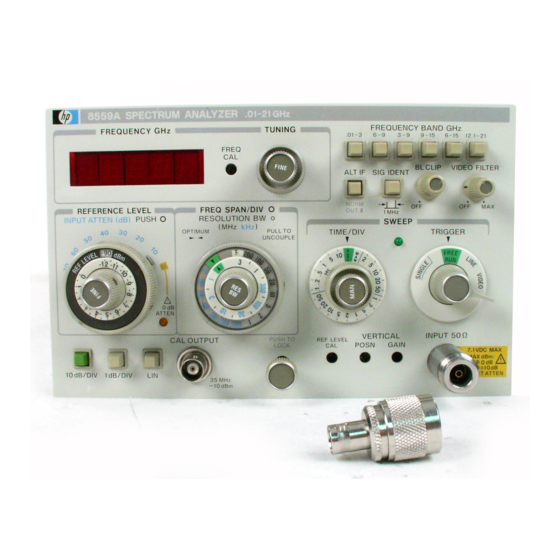
- Page 32 SWEEP TIME/DIV VIDEO FILTER indicates the spectrum analyzer center frequency SWEEP TRIGGER BASELINE CLIPPER with a resolution of 1 MHz. The HP 8559A can be VERT POSN HORIZONTAL POSI- used to measure signals over an amplitude range of TION VERT GAIN...
- Page 33 10 dB input 3-28. The front-panel adjustment procedure adapts attenuation the H P 8559A Spectrum Analyzer plug-in to a par- ticular display mainframe, and should be performed daily after instrument warm-up. The step-by-step Peak Pulse Power: 50 dBm (100W, >lOpsec...
- Page 34 SWEEP knob to center the CRT dot. plug-ins, set older OPTIMUM INPUT to -30 dBm. Leaving a dot on the CRT for pro- HP 853A Spectrum Analyzer longed periods at high intensity can Display burn the phosphor. WRITE TRACE A 3.
- Page 35 OPERATION MODEL 8559A 3-31. Frequency and Amplitude Adjustments 250 MHz CAL OUTPUT Connect the to the spectrum analyzer input, and center the signal Adjust VERTICAL POSN to align the CRT on the CRT with the TUNING control. The FREQUENCY MHz readout will indicate 250 trace with the bottom graticule line.
- Page 37 PERFORMANCE TESTS 4-4. Since a compatible display mainframe is required for operation of the HP Model 8559A Spec- performance of the instrument using the specifica- trum Analyzer plug-in, the specifications listed in tions in Section I as the performance standards. The...
- Page 38 COUNTER QENERATOR UODUL BNC TEE FIGURE 4-1. FREQUENCY SPAN ACCURACY TEST SETUP EQUIPMENT: ............Comb Generator HP 8406A ..........HP 5342A, Opt. 005 Frequency Counter ............Function Generator HP 33 10A ............BNC Tee HP 1250-078 1 ....... HP 1250-0780...
- Page 39 MODEL 8559A PERFORMANCE TESTS PERFORMANCE TESTS 4-11. FREQUENCY SPAN ACCURACY (Cont'd) PROCEDURE: 1. Set equipment controls as follows: Spectrum Analyzer: TUNING ........RESOLUTION BW OPTIMUM, coupled (pushed in) INPUTATTEN REFERENCELEVEL REFLEVELFINE ............Amplitude Scale 10 dB/DIV AUTO SWEEPTRIGGER ALTIF ..............
- Page 40 PERFORMANCE TESTS MODEL 8559A PERFORMANCE TESTS FREQUENCY SPAN ACCURACY (Cont'd) Adjust spectrum analyzer TUNING control to position one spectral line (from comb generator) at first graticule line (left-hand edge of display). Measure the error between 17th spectral line and 9th graticule line as shown in Figure 4-2.
- Page 41 MODEL 8559A PERFORMANCE TESTS PERFORMANCE TESTS FREQUENCY SPAN ACCURACY (Cont'd) NINTH GRATICULE LlNE FIRST GRATICULE LINE NINTH SPECTRAL LlNE COMB SIGNALS FIRST SPECTRAL LlNE CENTERFREQUENCY Set FREQ SPAN/DIV to 5 MHz. Adjust TUNING control to position one spectral line on the first graticule line.
- Page 42 PERFORMANCE TESTS MODEL 8559A PERFORMANCE TESTS FREQUENCY SPAN ACCURACY (Cont'd) 13. Set function generator frequency to 200 kHz 0.5%) using frequency counter. Connect function genera- tor output to comb generator MODULATION input. Set function generator OUTPUT LEVEL for a clean 200-kHz comb on the spectrum analyzer display.
- Page 43 TO A N A L Y Z E R ) ADAPTER ADAPTER FIGURE 4-4. TUNING ACCURACY TEST SETUP NOTE The HP 8350A Sweep Oscillator may be substituted for the HP 8620C in this procedure. EQUIPMENT ............Sweep Oscillator HP 8620C ...........
- Page 44 PERFORMANCE TESTS MODEL 8559A PERFORMANCE TESTS TUNING ACCURACY (Cont'd) 4-12. PROCEDURE: Set spectrum analyzer controls as follows: TUNING FREQ SPAN/DIV 200 kHz RESOLUTION BW OPTIMUM, coupled (pushed in) REFERENCE LEVEL 10 dBm REFLEVELFINE AUTO ............. SWEEPTRIGGER ..............ALTIF BLCLIP VIDEOFILTER Connect CAL OUTPUT signal of spectrum analyzer to INPUT 5W.
- Page 45 MODEL 8559A PERFORMANCE TESTS PERFORMANCE TESTS 4-12. TUNING ACCURACY (Cont'd) NOTE The 10 dB attenuator should be connected directly to the INPUT 50Q of the spectrum analyzer and the 11667A power splitter (no cable assembly should be used between attenuator and analyzer or power splitter).
- Page 46 PERFORMANCE TESTS MODEL 8559A PERFORMANCE TESTS RESIDUAL FM 4-13. SPECIFICATION: Less than 2 kHz peak-to-peak for a time interval 10.1 second; less than 2 kHz peak-to-peak in a 180-series display mainframe with 220/240 line voltage. DESCRIPTION: This test measures the inherent short-term instability (residual FM) of the LO system in the spectrum analyzer.
- Page 47 2. Connect OUTPUT of comb generator to spectrum analyzer INPUT 50Q as shown in Figure 4-5. NOTE The 8559A is sensitive to vibration. Be sure spectrum analyzer is in a vibration-free environment. 3. Adjust spectrum analyzer TUNING control to display 3.0 GHz signal produced by comb generator.
- Page 48 PERFORMANCE TESTS MODEL 8559A PERFORMANCE TESTS 4-14. NOISE SIDEBANDS SPECIFICATION: Noise sidebands are at least 70 dB below a CW signal, 30 kHz or more away from the signal with a 1 kHz resolution bandwidth and full video filtering. DESCRIPTION: A stable 1.8 GHz CW signal is applied at a...
- Page 49 MODEL 8559A PERFORMANCE TESTS PERFORMANCE TESTS 4-14. NOISE SIDEBANDS (Cont'd) Comb Generator: ..........100 MC COMB FREQUENCY ........INTERPOLATION AMPLITUDE 1 MHz ..........OUTPUT AMPLITUDE Full clockwise Connect equipment as shown in Figure 4-8. Adjust TUNING control to locate 1.8-GHz comb tooth on CRT Adjust REFERENCE LEVEL and REF LEVEL FINE controls to position peak of 1.8-GHz signal at top...
- Page 50 PERFORMANCE TESTS MODEL 8559A PERFORMANCE TESTS 4-15. RESOLUTION BANDWIDTH ACCURACY SPECIFICATION: Individual resolution bandwidth 3-dB points are calibrated to 30% for 3 MHz bandwidth). DESCRIPTION: Resolution bandwidth accuracy is measured in the linear mode to eliminate log amplifier errors. Since signal level at the 3-dB points (half-power points) is related to peak signal level by a voltage ratio of 0.707: 1 .O, a peak...
- Page 51 PERFORMANCE TESTS MODEL 8559A PERFORMANCE TESTS RESOLUTION BANDWIDTH ACCURACY (Cont'd) PROCEDURE: Part of this test must be performed with power supplied to the instrument and with protective covers removed. The test should be performed only by sewice-trained personnel who are aware of the hazards involved.
- Page 52 MODEL 8559A PERFORMANCE TESTS PERFORMANCE TESTS RESOLUTION BANDWIDTH ACCURACY (Cont'd) 5. Tune signal generator frequency until trace drops to 5 divisions above graticule baseline. Record signal generator frequency. 6. Tune signal generator frequency in direction opposite to that of step 5 until trace peaks (7.1 divisions above graticule baseline) and then drops to 5 divisions above graticule baseline.
- Page 53 MODEL 8559A PERFORMANCE TESTS PERFORMANCE TESTS 4-15. RESOLUTION BANDWIDTH ACCURACY (Cont'd) D l SPLAY S IGNA L GENERATOR RF OUTPUT FIGURE 4-10. RESOLUTION BANDWIDTH ACCURACY TEST SETUP, 30 kHz TO 1 kHz In the following procedure, the plug-in must be removed from the display mainframe and connected through the extender cable assembly.
- Page 54 PERFORMANCE TESTS MODEL 8559A PERFORMANCE TESTS RESOLUTION BANDWIDTH ACCURACY (Cont'd) Signal Generator: ..........COUNTERMODE ............ FREQUENCYTUNE ..........................OUTPUTLEVEL Connect equipment as shown in Figure 4-10. NOTE For early instruments that do not feature A16J3, a 21.4-MHz signal can be injected directly into the 300-MHz output (A1OJ1) of Third Converter Assem- bly A10.
- Page 55 MODEL 8559A PERFORMANCE TESTS PERFORMANCE TESTS RESOLUTION BAN DWlDTH ACCURACY (Cont'd) 19. Set RESOLUTION BW to 3 kHz, leaving FREQ SPAN/DIV set to 0. Repeat steps 14 through 17. Min. Actual Max. 2.5 kHz 3.45 kHz 20. Set RESOLUTION BW to 1 kHz, leaving FREQ SPAN/DIV set to 0. Repeat steps 14 through 17.
- Page 56 PERFORMANCE TESTS MODEL 8559A PERFORMANCE TESTS 4-16. RESOLUTION BANDWIDTH SELECTIVITY SPECIFICATION: < DESCRIPTION: The 60-dB bandwidth is measured for all resolution bandwidths. The 60- to 3-dB resolution bandwidth ratio (shape factor) is then computed for each bandwidth by dividing the 3-dB value (from the Resolution Bandwidth Accuracy test) into the 60-dB value.
- Page 57 MODEL 8559A PERFORMANCE TESTS PERFORMANCE TESTS 4-16. RESOLUTION BANDWIDTH SELECTIVITY (Cont'd) PROCEDURE: 1. Set equipment controls as follows: Spectrum Analyzer: TUNING RESOLUTIONBW INPUTATTEN REFERENCELEVEL REFLEVELFINE SWEEP TIME/DIV AUTO SWEEPTRIGGER ALTIF SIGIDENT BLCLIP VIDEO FILTER 12 o'clock Signal Generator: COUNTERMODE FREQUENCYTUNE OUTPUTLEVEL 2.
- Page 58 PERFORMANCE TESTS MODEL 8559A PERFORMANCE TESTS RESOLUTION BANDWIDTH SELECTIVITY (Cont'd) 4-16. Tune signal generator in direction opposite to that of step 4 until trace peaks (top graticule line) and then drops to 2 divisions above graticule baseline. Record signal generator frequency.
- Page 59 MODEL 8559A PERFORMANCE TESTS PERFORMANCE TESTS RESOLUTION BANDWIDTH SELECTIVITY (Cont'd) Signal Generator: COUNTERMODE FREQUENCYTUNE OUTPUTLEVEL Connect equipment as shown in Figure 4-12. SPECTRUM ANALYZER INPUT ADAPTER ADAPTER FIGURE 4-12. RESOLUTION BANDWIDTH SELECTIVITYTESTSETUP, 100 kHzTO 3 MHz Adjust spectrum analyzer TUNING to locate peak of 35-MHz signal on CRT Reduce signal generator output if necessary.
- Page 60 PERFORMANCE TESTS MODEL 8559A PERFORMANCE TESTS RESOLUTION BANDWIDTH SELECTIVITY (Cont'd) Set RESOLUTION BW to 300 kHz, leaving FREQ SPAN/DIV set to 0 . Repeat steps 14 through 18. Set RESOLUTION BW to 1 MHz, leaving FREQ SPAWDIV set to 0. Repeat steps 14 through 18.
- Page 61 ..........HP 909A, Opt. 01 NOTE The HP 853A Spectrum Analyzer Display may be substituted for the HP NOTE This test can be performed with no input termination if INPUT ATTEN is set to 20 dB. Note that the input attenuation must then be taken into consider- ation in establishing the equivalent REFERENCE LEVEL control setting for the measurement.
- Page 62 MODEL 8559A PERFORMANCE TESTS PERFORMANCE TESTS 4-17. AVERAGE NOISE LEVEL (Cont'd) PROCEDURE: 1. Set spectrum analyzer controls as follows: TUNING RESOLUTION BW 3 MHz, uncoupled .............. INPUTATTEN REFERENCE LEVEL - 60 dBm REF LEVEL FINE ............AUTO SWEEPTRIGGER ..............ALTIF...
- Page 63 PERFORMANCETESTS MODEL 8559A PERFORMANCE TESTS 4-17. AVERAGE NOISE LEVEL (Cont'd) NOTE Do not tune above 18.0 GHz for this step. 11. Repeat steps 2 through for the frequency range of 18.0 21.0 GHz. 12. Repeat entire procedure with ALT IF on.
- Page 64 Termination, Type N (m) HP 909A, Opt. 012 NOTE The HP 853A Spectrum Analyzer Display may be substituted for the HP NOTE This test can be performed with no input termination if INPUT ATTEN is set to 20 dB. Note that the input attenuation must then be taken into consider- ation in establishing the equivalent REFERENCE LEVEL control setting for the measurement.
- Page 65 NOTE Residual responses are often visible within 10 MHz of the HP 8559A LO feedthrough signal (25 MHz with ALT IF selected). These residual responses are not within the instrument's specified frequency range and should be excluded from consideration in this performance test.
- Page 66 PERFORMANCE TESTS MODEL 8559A PERFORMANCE TESTS FREQUENCY RESPONSE 4-19. SPECIFICATION: Frequency response measured with 0 or 10 dB of input attenuation includes input attenuator flatness, mixer flatness, and band-to-band amplitude variation. Table 4-6 shows the frequency response specifications. TABLE 48. FREQUENCY RESPONSE SPEClFiCATiONS...
- Page 67 FREQUENCY RESPONSE (Cont'd) NOTE The HP 853A Spectrum Analyzer Display is not recommended for use in this procedure. The HP 8350A Sweep Oscillator may be substituted for the HP 8620C in this procedure, if necessary. EQUIPMENT: Variable Persistence/Storage Display ............
- Page 68 PERFORMANCE TESTS MODEL 8559A PERFORMANCE TESTS FREQUENCY RESPONSE (Cont'd) 4-19. Sweep Oscillator: CW Frequency .... MARKERS .... SWEEP MODE AUTO (or TIME) ..SWEEP TRIGGER SWEEP-TIME-SEC .... RF OFF-ON ALC Switch ... POWER LEVEL Midrange RF BLANKING (Rear Panel) ..
- Page 69 Remove 0.01 Plug-in. Select band 4 (2.0 22 GHz) on HP 8620C sweep oscillator. 13. Set sweep oscillator to CW with frequency of 2.1 GHz and use CW control to position signal on 8th vertical graticule line of spectrum analyzer display. Adjust ALC GAIN control for leveled sweep oscillator...
- Page 70 Minimum divisions NOTE It is normal for the HP 8559A to exhibit baseline lift with an input signal at approximately 3.0075 GHz(2.9925 with ALT IF selected). Adjust sweep oscil- lator sweep range as necessary to avoid baseline lift during frequency response measurements.
- Page 71 MODEL 8559A PERFORMANCE TESTS PERFORMANCE TESTS FREQUENCY RESPONSE (Cont'd) 4.19. Frequency Response, 3 18 GHz NOTE For the higher frequency bands, multiple responses may appear on spec- trum analyzer display during frequency response measurement. Adjust INTENSITY control as necessary for optimum display of in-band signal peaks.
- Page 72 PERFORMANCE TESTS MODEL 8559A PERFORMANCE TESTS 4-19. FREQUENCY RESPONSE (Cont'd) Select 9 spectrum analyzer TUNING control to reposition tuning marker. Trigger another sweep. Record greatest positive and greatest negative deviation of signal peaks from center horizontal graticule line (neglect devia- tions caused by tuning marker).
- Page 73 MODEL 8559A PERFORMANCE TESTS PERFORMANCE TESTS 4-19. FREQUENCY RESPONSE (Cont'd) 26. Subtract mean deviation of step 16 from maximum and minimum values recorded in step 25. Frequency response for 12.1 18 GHz portion of 12.1 21 GHz frequency band should not exceed 2.3 dB...
- Page 74 PERFORMANCE TESTS MODEL 8559A PERFORMANCE TESTS 4-19. FREQUENCY RESPONSE (Cont'd) TABLE 4-7. CORRECTING FOR FREQUENCY RESPONSE OF SIGNAL SOURCE Deviation from Power Meter Power Sum of Deviation Frequency Center Graticule lndication Deviation* Deviations from Mean Line (divisions or dB) 18.0 *deviation relative to power meter indication at 18.0 GHz, recorded in step 27.
- Page 75 PERFORMANCE TESTS MODEL 8559A PERFORMANCE TESTS 4-20. SPECIFICATION: Gain compression is less than 0.5 dB for a 10 dBm input level with 0 dB attenuation. DESCRIPTION: Gain compression is measured by changing the power level at the spectrum analyzer input from -20 dBm to 10 dBm.
- Page 76 PERFORMANCE TESTS MODEL 8559A PERFORMANCE TESTS (Cont'd) 4-20. PROCEDURE: 1. Set equipment controls as follows: Spectrum Analyzer: .............. TUNING FREQ SPAN/DIV 100 kHz RESOLUTION BW 300 kHz, uncoupled INPUTATTEN REFERENCE LEVEL 10 dBm ............REFLEVELFINE Amplitude Scale 10 dB/DIV SWEEP TIME/DIV...
- Page 77 MODEL 8559A PERFORMANCE TESTS PERFORMANCE TESTS 4-20. Adjust signal generator OUTPUT LEVEL control for a power meter reading of - ( - 20 spectrum analyzer connector). Set spectrum analyzer INPUT ATTEN control to and REF LEVEL FINE control to Adjust REF LEVEL CAL control to place peak of signal at refer- ence graticule line of step 4.
- Page 78 PERFORMANCE TESTS MODEL 8559A PERFORMANCE TESTS BANDWIDTH SWITCHING (AMPLITUDE VARIATION) SPECIFICATION: < Bandwidths 3 MHz to 300 kHz: < Bandwidths 3 MHz to 1 kHz: DESCRIPTION: The CAL OUTPUT signal is applied to INPUT 50Q connector and displayed on CRT. The peak of displayed 35-MHz signal is centered on CRT and adjusted for a vertical deflection of several divisions.
- Page 79 PERFORMANCE TESTS MODEL 8559A PERFORMANCE TESTS BANDWIDTH SWITCHING (AMPLITUDE VARIATION) (Cont'd) TABLE 4-8. BANDWIDTH SWITCHING (AMPLITUDE VARIATION) Overall Variation Overall Variation Between FREQ Amplitude RESOLUTION Between 3 MHz and 3 MHz and 300 kHz Deviation kHz RESOLUTION RESOLUTION BW Settings (dB)
- Page 80 SPECTRUM ANALYZER ADAPTER ATTENUATOR STEP ATTENUATOR FIGURE 4-17. INPUT ATTENUATOR ACCURACY TEST SETUP EQUIPMENT: Step Attenuator (10 dB/step) HP 355D, Opt. H82 10-dB Attenuztor HP 8491B, Opt. 010 Adapter, Type N (m) to BNC (f) (2 required) HP 1250-0780...
- Page 81 PERFORMANCE TESTS MODEL 8559A PERFORMANCE TESTS 4-22. INPUT ATTENUATOR ACCURACY (Cont'd) PROCEDURE: Connect equipment as shown in Figure and set controls as follows: 4-17 Spectrum Analyzer: ..........FREQUENCY BAND GHz TUNING ............RESOLUTIONBW INPUTATTEN ............REFERENCELEVEL REFLEVELFINE AUTO SWEEPTRIGGER ALTIF...
- Page 82 PERFORMANCE TESTS MODEL 8559A PERFORMANCE TESTS 4.22. INPUT ATTENUATOR ACCURACY (Cont'd) TABLE 4-9. INPUT AllENUATOR ACCURACY INPUT ATTEN Amplitude Step Step Attenuator Corrected Setting Attenuator Deviation Error Deviation (Calibration)" Setting (dB) > For example, 9.99 dB *Attenuations dial settings are positive (+). Attenuations dial settings are negative (-).
- Page 83 MODEL 8559A PERFORMANCE TESTS PERFORMANCE TESTS 4-23. REFERENCE LEVEL ACCURACY SPECIFICATION: Step Accuracy (steps referenced with 0 dB input attenuation): 0.5 dB 10 dBm to 80 dBm: Vernier Accuracy: 0.5 dB DESCRIPTION: The reference level accuracy is tested over the range of...
- Page 84 PERFORMANCE TESTS MODEL 8559A PERFORMANCE TESTS REFERENCE LEVEL ACCURACY (Cont'd) 4-23. PROCEDURE: Step Accuracy in Log Mode Set equipment controls as follows: Spectrum Analyzer: TUNING FREQ SPAN/DIV 100 kHz RESOLUTION BW 30 kHz, uncoupled INPUTATTEN REFERENCE LEVEL 10 dBm REFLEVELFINE...
- Page 85 PERFORMANCE TESTS MODEL 8559A PERFORMANCE TESTS 4-23. REFERENCE LEVEL ACCURACY (Cont'd) TABLE 4-10. IF GAIN ACCURACY IN LOG MODE Corrected REFERENCE Step Deviation from Step Attenuator LEVEL Attenuator 6th Division Error (Calibration)" Deviation Setting (dBm) Setting (dB) > *Attenuations dial settings are positive...
- Page 86 PERFORMANCE TESTS MODEL 8559A PERFORMANCE TESTS 4-23. REFERENCE LEVEL ACCURACY (Cont'd) TABLE 4-11. IF GAIN ACCURACY IN LINEAR MODE REFERENCE Step Attenuator Deviation from Deviation from Step Attenuator Corrected LEVEL 6th Division 6th Division Deviation Setting Error Setting (d Bm) Linear Mode (div.)
- Page 87 MODEL 8559A PERFORMANCE TESTS PERFORMANCE TESTS 4-23. REFERENCE LEVEL ACCURACY (Cont'd) Vernier Accuracy 9. Replace 10-dB step attenuator with 1-dB step attenuator. Set spectrum analyzer controls as follows: FREQUENCY BAND GHz .............. TUNING ............RESOLUTION BW 300 kHz, uncoupled ..............
- Page 88 PERFORMANCE TESTS MODEL 8559A PERFORMANCE TESTS 4-24. SWEEP TlME ACCURACY SPECIFICATION: There are 20 selectable and calibrated sweep times in a 1-2-5 sequence from 2 pec/DIV to 10 sec/DIV (excluding 2 sec/DIV) Sweep time accuracy: 20% for 5 and 10 sec/DIV)
- Page 89 PERFORMANCE TESTS MODEL 8559A PERFORMANCE TESTS 4-24. SWEEP TIME ACCURACY (Cont'd) PROCEDURE: 1. Set equipment controls as follows: Spectrum Analyzer: ..........FREQUENCY BAND GHz TUNING ..........RESOLUTION BW 3 MHz, uncoupled INPUTATTEN ............ REFERENCELEVEL REFLEVELFINE .............. Amplitude Scale ............AUTO .............
- Page 90 0, leaving RESOLUTION BW control at 3 MHz setting. Set SWEEP TIME/DIV control to 2 4. Set AM switch of HP 8640B to AC position. Adjust function generator AMPLITUDE control and signal generator AM MODULATION control for 50 percent modulation as indicated on the signal generator meter.
- Page 91 P E R F O R M A N C E TESTS MODEL 8559A PERFORMANCE TESTS 4-24. SWEEP TIME ACCURACY (Cont'd) T A B L E 4-14, S W E E P T I M E A C C U R A C Y , 2pSECTHROUGH 10 MSEC...
- Page 92 PERFORMANCE TESTS MODEL 8559A PERFORMANCE TESTS SWEEP TIME ACCURACY (Cont'd) 4-24. W E E P Sweep Time Setting Minimum Actual Maximum 20 msec 0.180 sec 0.220 sec 50 msec 0.450 sec se c 0.550 sec 0.90 sec 1.10 sec 1.80 sec 2.20 sec...
- Page 93 MODEL 8559A PERFORMANCE TESTS PERFORMANCE TESTS 4-25. CALIBRATOR OUTPUT ACCURACY SPECIFICATION: 10 dBm Amplitude: Frequency: 35 MHz DESCRIPTION: The frequency of the calibrator output signal is measured with a microwave counter. The calibrator output level is measured using a power meter.
- Page 94 STEP ATTENUATOR ADAPTER FIGURE 4-22. DISPLAY FIDELITY TEST SETUP EQUIPMENT ........HP 355D, Opt. H82 Step Attenuator (10 dB/step) Adapter, Type N (m) to BNC (f) (2 required) HP 1250-0780 ..........HP 1 1001 A Cable, BNC to Banana Plug...
- Page 95 MODEL 8559A PERFORMANCE TESTS PERFORMANCE TESTS DISPLAY FIDELITY (Cont'd) 4-26. FREQ SPAN/DIV 500 kHz RESOLUTION BW 300 kHz, uncoupled INPUT ATTEN 10 dB REFERENCE LEVEL .............. REFLEVELFINE .............. SWEEP TIME/DIV AUTO SWEEPTRIGGER ..............ALTIF BL CLIP VIDEO FILTER Digital Voltmeter: ..............
- Page 96 PERFORMANCE TESTS MODEL 8559A PERFORMANCE TESTS 4-26. DISPLAY FIDELITY (Cont'd) TABLE 4-16. AMPLITUDE LOG DISPLAY ACCURACY Difference Theoretical Corrected Attenuator D V M Theoretical Reading Subtracted Between D V M Setting Reading Reading From Corrected Adjacent Reading* D V M Reading Readings offset recorded in step 2.
- Page 97 MODEL 8559A PERFORMANCE TESTS PERFORMANCE TESTS 4-26. DISPLAY FIDELITY (Cont'd) Algebraically subtract each converted reading (Theoretical Reading Subtracted from Corrected DVM Reading) from previous converted reading. Record results in Table 4-16 (see sample computations). Maxi- mum difference between adjacent readings should not exceed...
- Page 98 MODEL 8559A PERFORMANCE TESTS TABLE 4-18. PERFORMANCE TEST RECORD (1 OF 4) Tested by Model 8559A Spectrum Analyzer .01-21 GHz Serial No. Date Results Para. Test Description Actual Frequency Span Accuracy 3. 200 MHz FREQ SPANIDIV -0.4 div 4. 100 MHz FREQ SPANIDIV -0.4 div...
- Page 99 MODEL 8559A PERFORMANCE TESTS TABLE 4-18. PERFORMANCE TEST RECORD (2 OF 4) Results Para. Test Description Actual 4.13. Residual FM 1.4 div 6. Peak-to-Peak Variation of Trace (2 kHz1O.l sec) Noise Sidebands 7.0 div down 6. Noise Sidebands (-70 dB) Resolution Bandwidth Accuracy 7.
- Page 100 PERFORMANCE TESTS MODEL 8559A TABLE 4-18. PERFORMANCE TEST RECORD (3 OF 4) Results Para. Test Description Min. Actual Max. Residual Responses 6. Residual Responses, .Ol GHz to 3 GHz 7. Residual Responses, .Ol GHz to 3 GHz (ALT IF) Frequency Response 15.
- Page 101 MODEL 8559A PERFORMANCE TESTS TABLE 4-18. PERFORMANCE TEST RECORD (4 OF 4) Results Para. Test Description Actual Max. Min. Sweep Time Accuracy 2.20 psec 7. Sweep Time, 2 psecldiv 1.80 psec 5.50 psec 8. Sweep Time, 5 psec/div 4.50 psec Sweep Time, 10 psecldiv 9 .OO psec...
- Page 103 5-2. This section describes the adjustments used to restore the HP 8559A to its peak operating condition after a repair or to compensate for changes resulting from component aging. Illustrations showing the appropriate test setups are included in the adjust- 5-7.
- Page 104 5-15. FACTORY SELECTED COMPONENTS 5-13. 5-16. Table 5-3 is a list of factory selected compo- nents used in the H P 8559A. The components are listed by reference designator, related adjustment when the troubleshooting information in Section paragraph, and by basis of selection. Factory...
- Page 105 ADJUSTMENTS MODEL 8559A Adjustment Adjustment Reference Description Designator Paragraph Name Adjusts DPM high indication. A1 A2R28 GAIN Adjusts DPM low indication. OFFSET A1 A2 R29 Adjusts Second Converter output match. A5 L2 2nd MIXER MATCH Adjusts First I F Bandpass Filter Response.
- Page 106 MODEL 8559A ADJUSTMENTS TABLE 5-1. ADJUSTABLE COMPONENTS (2 OF 3) Adjustment Reference Adjustment Description Designator Paragraph Name Adjusts symmetry of second crystal bandwidth filter stage. Adjusts centering of second LC bandwidth filter stage LC CTR Adjusts centering of second crystal bandwidth filter stage.
- Page 107 MODEL 8559A ADJUSTMENTS TABLE 5-1. ADJUSTABLE COMPONENTS (3 OF 3) Adjustment Reference Description Name Designator Paragraph Adjusts dc offset circuitry at output of Log Amplifier LOG GAIN Assembly A14 for 10 dB steps in log mode. 1 dB (offset) Adjusts LOG 10 dB/DIV translation.
- Page 108 ADJUSTMENTS MODEL 8559A TABLE 5-2. RELATED ADJUSTMENTS Paragraph Perform the Following Related Adjustments or Repaired Number DPM Display Frequency Display Adjustments DPM Driver Frequency Display Adjustments Front Panel Switch First Converter Adjustments Assembly CAL OUTPUT and REF LEVEL CAL Adjustments...
- Page 109 MODEL 8559A ADJUSTMENTS TABLE 53. FACTORY SELECTED COMPONENTS IN ALPHA-NUMERICALORDER Reference Reference Basis of Selection Basis of Selection Designator Designator Selected t o equalize feedback between Adjusts bias on DPM Clock Oscillator. LC stages (not field selectable). Selected to provide delay compensation Selected to optimize 3 MHz to 1 MHz for main coil sweeps.
- Page 110 ADJUSTMENTS MODEL 8559A TABLE 5-4. HP PART NUMBERS OF STANDARD VALUE REPLACEMENT COMPONENTS (1 OF 3) CAPACITORS R A N G E : 1 t o 24 pF TYPE: Tubular 680 pF R A N G E : T O L E R A N C E :...
- Page 111 MODEL 8559A ADJUSTMENTS TABLE RESISTORS RANGE: 10 464K Ohms TYPE: Fixed-Film WATTAG E 1 25°C TOLERANCE: %1.0% Value Value Value HP Part Number HP Part Number HP Part Number 10.0 2 1.5K 12.1 13.3 14.7 17.8 19.6 21.5 23.7 26.1 28.7...
- Page 112 ADJUSTMENTS MODEL 8559A TABLE 5-4. HP PART NUMBERS OF STANDARD VALUE REPLACEMENTCOMPONENTS (3 OF3) RESISTORS RANSE: 10 Ohms TYPE: Fixed-Film 125°C WATTAGE: TOLERANCE: Value HP Part HP Part Value Value HP Part HP Part Number Number Number Number 6.8 1 K...
- Page 113 MODEL 8559A ADJUSTMENTS ADJUSTMENTS 5-17. POWER SUPPLY CHECKS AND ADJUSTMENTS REFERENCE: A7, A8, A9 Schematics DESCRIPTION: (dependent) - 12V power supply is then checked for proper dc output (with less than 50 mV variation) while the spectrum analyzer is tuned from 10 MHz to 3 GHz. The width Control Assembly A9 and the VO (Varactor Offset) voltage on Marker Assembly A8 are then adjusted.
-
Page 114: Freq Span/Div
ADJUSTMENTS MODEL 8559A ADJUSTMENTS 5-17. POWER SUPPLY CHECKS AND ADJUSTMENTS (Cont'd) PROCEDURE: 1. Set spectrum analyzer controls as follows: TUNING ............FREQ SPAN/DIV F (full) ..........RESOLUTION BW Optimum, coupled ............REFERENCE LEVEL REFLEVELFINE ............Amplitude Scale 10 dB/DIV ............ - Page 115 MODEL 8559A ADJUSTMENTS ADJUSTMENTS 5-17. POWER SUPPLY CHECKS AND ADJUSTMENTS (Cont'd) NOTE The two following voltage adjustments, must be performed while the spectrum analyzer is still cold (during first five minutes after turn-on). If the instrument has been operating longer than five minutes, turn off the display mainframe, remove A8 and A9 assemblies, and let them cool on bench for 15 minutes.
- Page 116 ADJUSTMENTS MODEL 8559A ADJUSTMENTS CALIBRATED SWEEP TIME ADJUSTMENT 5-18. REFERENCE: Schematic DESCRIPTION: A counter is used to adjust the time interval of the 1 millisecond per division and 5 milliseconds per division sweep times. Calibrated sweep times from 0.1 milliseconds through 50 milliseconds are then checked using the counter time-interval (T.
-
Page 117: Video Filter Off
Set equipment controls as follows: NOTE If an HP 853A Spectrum Analyzer Display mainframe is used, and a sweep time faster than 10 msec is selected, an error message will appear on the analyzer's CRT and the analyzer will go into mixed mode. - Page 118 MODEL 8559A ADJUSTMENTS ADJUSTMENTS 5-18. CALIBRATED SWEEP TIME ADJUSTMENT (Cont'd) NOTE In early instruments, A9R13 is labeled "2 ms." The adjustment of A9R13, however, should be performed with SWEEP TlMUDlV set at 5 ms. spectrum analyzer SWEEP TIME/DIV control to 5 msec. Readjust counter SENSITIVITY controls as necessary and adjust 5 ms potentiometer A9R13 for a time interval indication of 50.00...
- Page 119 EQUIPMENT: Signal Generator H P 8640B Digital Voltmeter HP 3456A Step Attenuator (10-dB/step) HP 355D, Opt. H82 Step Attenuator (1-dB/step) H P 355C, Opt. H80 Cable Assembly, Banana Plug to BNC (m) HP 1-1001A Adapter, Type N (m) to BNC...
- Page 120 2. Set 1-dB step attenuator to 10 dB and 10-dB step attenuator to 0 dB. Remove AlOWl (blue cable) from NOTE The HP 355C 10 dB attenuation is included to compensate for 10 dB of gain on Step Gain Assembly A12 with the TEST-NORM switch in TEST.
- Page 121 MODEL 8559A ADJUSTMENTS ADJUSTMENTS Disconnect signal generator output from step attenuator. Adjust spectrum analyzer VERTICAL POSN control to position signal trace at bottom CRT graticule line. Measure dc offset voltage at Al5TP1 and record. Connect signal generator to step attenuator and adjust signal generator FINE TUNE control to peak signal on CRT display.
- Page 122 MODEL 8559A ADJUSTMENTS ADJUSTMENTS 5-19. LOG AMPLIFIER LOG AND LINEAR ADJUSTMENTS (Cont'd) TABLE 5-6. LOG FIDELITY CHECK Theoretical Difference Corrected Step Theoretical Reading Subtracted Between Test Attenuator Adjacent Limits Reading from Corrected Reading* Setting Readings*" DVM Reading DVM reading minus offset recorded in step 4.
- Page 123 MODEL 8559A ADJUSTMENTS ADJUSTMENTS 5-19. LOG AMPLIFIER LOG AND LINEAR ADJUSTMENTS (Cont'd) Linear Output and Linear Step Gain 20. Disconnect AlOWl from step attenuator and reconnect to A5J2. When reconnecting A1OW1 to A5J2, do not tighten to over 6 inch pounds of torque;...
- Page 124 ADJUSTMENTS MODEL 8559A ADJUSTMENTS 5-19. LOG AMPLIFIER LOG AND LINEAR ADJUSTMENTS (Cont'd) Log Gain 24. Set spectrum analyzer controls as follows: REFERENCE LEVEL 50 dBm 25. Set 10-dB step attenuator to 0 dB. Retune spectrum analyzer to peak signal. Adjust signal generator...
- Page 125 MODEL 8559A ADJUSTMENTS ADJUSTMENTS 5-19. LOG AMPLIFIER LOG AND LINEAR ADJUSTMENTS (Cont'd) TABLE 5-10, LOG AMPLIFIER OUTPUT LIMITS Theoretical Difference Step Corrected D V M Test Theoretical Reading Subtracted Between Attenuator D V M Reading Limits Reading from Corrected Adjacent...
- Page 126 ADJUSTMENTS MODEL 8559A ADJUSTMENTS 5-20. REFERENCE: A 15 Schematic DESCRIPTION: Reference is set in 10 dB/DIV amplitude scale and 1 dB offset is adjusted in 1 dB/DIV for the same full display reference. D l SPLAY SPECTRUM ANALYZER EXTENDER CABLE...
- Page 127 HP 8559A is properly installed in display mainframe. 7. Set Amplitude Scale to 1 dB/DIV. Adjust A15R1 1 dB OFFSET for a trace 0.5 division down from top...
- Page 128 Extender Cable Assembly HP 5060-0303 NOTE A crystal short consists of a .O1 pF capacitor (HP Part Number 0160-0161) and a 90.9 ohm resistor (HP Part Number 0757-0400) connected in series. Two square terminal connectors (HP Part Number 0362-0265) are used to...
- Page 129 MODEL 8559A ADJUSTMENTS ADJUSTMENTS 5-21. BANDWIDTH FILTER ADJUSTMENTS (Cont'd) TERMINAL CONNECTORS FIGURE CRYSTAL SHORT CONFIGURATION PROCEDURE: NOTE Allow 30 minutes warmup time before performing adjustments. Set spectrum analyzer controls as follows: FREQUENCYBAND TUNING RESOLUTIONBW INPUTATTEN REFERENCELEVEL Amplitude Scale SWEEPTRIGGER Crystal Alignment Connect equipment as shown in Figure 5-5.
- Page 130 ADJUSTMENTS MODEL 8559A ADJUSTMENTS 5-21. BANDWIDTH FILTER ADJUSTMENTS (Cont'd) Center the signal with TUNING control. Using REF LEVEL FINE control, place signal peak at 7.1 divisions (0.9 division from top graticule line). Adjust A9R85 LC until signal is five divisions wide at the fifth graticule line (1 MHz wide at 3-dB points).
- Page 131 MODEL 8559A ADJUSTMENTS ADJUSTMENTS 5-21. BANDWIDTH FILTER ADJUSTMENTS (Cont'd) CHECK CENTERING HERE (SPIKE IS CRYSTAL RINGING) CHECK SYMMETRY HERE (LOW ON SKIRTS) FIGURE ADJUSTING CRYSTAL SYMMETRY AND CRYSTAL CENTERING Remove crystal short from A13TP 1 /TP2 and connect it across A1 3TP4/TP5.
- Page 132 24. Set RESOLUTION BW control to 100 kHz. Jumper A9TP6 to A9TP8. This forces the BW7 line to NOTE When Bandwidth Filter Assemblies A l l and A13 are installed with covers in place, midget copper alligator clips (HP Part Number 1400-0483) can be used to short test points to the cover. Perform preliminary LC filter adjustments...
- Page 133 MODEL 8559A ADJUSTMENTS ADJUSTMENTS BANDWIDTH FILTER ADJUSTMENTS (Cont'd) 5-21. 26. Short to ground A1 lTP3, A1 lTP6, and A13TP3. Set RESOLUTION BW to 100 kHz and set FREQ 27. Center signal on CRT with TUNING control. Adjust A13C45 LC CTR for symmetrical bandpass display on CRT Use FINE TUNING control to keep crystal spike centered.
- Page 134 ADJUSTMENTS MODEL 8559A ADJUSTMENTS 5-21. BANDWIDTH FILTER ADJUSTMENTS (Cont'd) Adjust FINE TUNING and REF LEVEL FINE controls for a centered signal at 7 divisions from bottom graticule line. Remove shorts from A13TP3 and A13TP6 and center signal with FINE TUNING control. Adjust Remove shorts from A1 lTP3 and A1 1TP6.
- Page 135 MODEL 8559A ADJUSTMENTS ADJUSTMENTS 5-22. REFERENCE: A9 Schematic DESCRIPTION: The 3-dB bandwidths for the 3 MHz through the 30 kHz RESOLUTION BW settings are adjusted using the CAL OUTPUT as the signal source. The 3-dB bandwidths for the 10 kHz, 3 kHz, and 1 kHz RESOLUTION BW settings are adjusted by injecting a stable 321.4 MHz signal into the Third Converter (A10) of the spectrum...
- Page 136 ADJUSTMENTS MODEL 8559A ADJUSTMENTS 5-22. 3-dB BANDWIDTH ADJUSTMENTS (Cont'd) PROCEDURE: Set spectrum analyzer controls as follows: FREQUENCYBAND TUNING RESOLUTIONBW INPUTATTEN ............REFERENCELEVEL SWEEPTRIGGER VIDEOFILTER BASELINECLIPPER ....853A (if used) TRACE A & TRACE B STORE BLANK (ANALOG DISPLAY) Connect CAL OUTPUT to spectrum analyzer INPUT Set a 7.1 division signal level on display with REF LEVEL FINE control.
- Page 137 10 dBm output level. The 10 dB step attenuator between BNC tee and frequency counter can be elirni- nated. 11. Set H P 8559A RESOLUTION BW to MHz. Tune signal generator to peak signal on CRT display (near 21.4 MHz) (321.4 MHz if injecting into AlOWl). Adjust the output level of signal generator to place the signal at 7.1 divisions.
- Page 138 ADJUSTMENTS MODEL 8559A ADJUSTMENTS 5-22. 3-dB BANDWIDTH ADJUSTMENTS (Cont'd) Adjust A9R72 XTL to bring signal level to the fifth graticule line (three divisions from the top graticule line). Increase signal generator frequency until signal on CRT display peaks and then decreases to the fifth graticule line.
- Page 139 MODEL 8559A ADJUSTMENTS ADJUSTMENTS 5-22. 3-dB BANDWIDTH ADJUSTMENTS (Cont'd) Increase signal generator frequency until signal on CRT display decreases to the fifth graticule line. Record the counter frequency. Compare new frequency with frequency originally noted in step 25. The difference between the two fre-...
- Page 140 ADJUSTMENTS MODEL 8559A ADJUSTMENTS 5-23. RF GAlN ADJUSTMENT REFERENCE: A12 Schematic DESCRIPTION: The RF gain (sensitivity) of Step Gain Assembly A12 is adjusted by injecting a 21.4 MHz signal at XAlOPl. Third Converter Assembly A10 is removed and replaced with a special extender board for applying the 21.4 MHz signal from the signal generator.
- Page 141 RF GAIN ADJUSTMENT (Cont'd) NOTE To make special extender board, solder 51.1 ohm resistor from pin 18 to pin 22 of standard 24 pin extender board, HP Part No. 5060-0258. Leave resistor leads long for easy connection of clip leads. PROCEDURE: 1.
- Page 142 ADJUSTMENTS MODEL 8559A ADJUSTMENTS 5-23. RF GAlN ADJUSTMENT (Cont'd) When reconnecting A1OW1 to A5J2, exercise caution; the connector should not be torqued more than 6 inch-pounds, othewise damage to A5J2 will result. NOTE Front panel VERTICAL GAlN and POSN control settings can affect the volt- age measured at A15TP1.
- Page 143 D l SPLAY STEP ATTENUATOR FIGURE 5-10. STEP GAlN ADJUSTMENTS TEST SETUP EQUIPMENT: ............Signal Generator HP 8640B ........HP 355C, Option H80 Step Attenuator (1 dB/Step) ........Step Attenuator (10 dB/Step) HP 355D, Option H82 ............Digital Voltmeter ......... HP 1250-0780 Adapter, Type N (m) to BNC ..........
- Page 144 ADJUSTMENTS MODEL 8559A ADJUSTMENTS 5-24. STEP GAIN ADJUSTMENTS (Cont'd) PROCEDURE: Set spectrum analyzer controls as follows: ............RESOLUTIONBW INPUTATTEN ........................AUTO ............. SWEEPTRIGGER VIDEO FILTER Connect equipment as shown in Figure 5-10. Connect signal generator tuned to 321.4 MHz with approxi- mately 30 dBm output to one side of a 1 dB/step attenuator.
- Page 145 MODEL 8559A ADJUSTMENTS ADJUSTMENTS 5-24. STEP GAIN ADJUSTMENTS (Cont'd) NOTE Some video filtering might help reduce noise. Set VIDEO FILTER control so noise is reduced, but the signal amplitude remains unchanged. 16. Adjust A12R29 40 D adjustment for signal level one division from top graticule line.
- Page 146 ADJUSTMENTS MODEL 8559A ADJUSTMENTS 5-25. FIRST CONVERTER ADJUSTMENTS REFERENCE: A3, A4, AS, A6, and A7 Schematics DESCRIPTION: The First LO (A6 YTO) is adjusted by monitoring the YTO output at the RF input connector (LO emission) and the tuning voltage (TUNE) output of the A7 Frequency Control board, and adjusting the YTO low-end fre-...
- Page 147 MODEL 8559A ADJUSTMENTS ADJUSTMENTS 5-25. FIRST CONVERTER ADJUSTMENTS (Cont'd) First LO Adjustments 2. Connect DVM to A7TP6 TUNE. 3. Set spectrum analyzer controls as follows: INPUT ATTEN FREQ SPAN/DIV ALTIF 4. Connect frequency counter to spectrum analyzer RF Input. 5. Jumper A16TPl DIODE BIAS to ground. A16TP1 is located on the motherboard through a hole in the analyzer left side gusset.
-
Page 148: Trigger
ADJUSTMENTS MODEL 8559A ADJUSTMENTS 5-25. FIRST CONVERTER ADJUSTMENTS (Cont'd) Alternate IF First LO Shift Check 15. Press front-panel ALT IF pushbutton IN to activate alternate IE 16. Verify YTO frequency shift according to Table 5-12. ABLE 5-12. FIRST LO SHIFT CHECK... - Page 149 MODEL 8559A ADJUSTMENTS ADJUSTMENTS 5-25. FIRST CONVERTER ADJUSTMENTS (Cont'd) Adjust front-panel TUNING FINE control to place a comb tooth on the first vertical graticule line of the CRT display. Adjust A7R92 FM to place a comb tooth on the ninth vertical graticule line of the CRT display.
- Page 150 ADJUSTMENTS MODEL 8559A ADJUSTMENTS FIRST CONVERTER ADJUSTMENTS (Cont'd) 5-25. Set FREQ SPAN/DIV to 1 MHz. Note position of comb tooth. Adjust A7R81 (MO) to place comb tooth midway between position noted in step 38 and center graticule line. Set FREQ SPAN/DIV to 2 MHz.
- Page 151 MODEL 8559A ADJUSTMENTS ADJUSTMENTS 5-26. SECOND CONVERTER ADJUSTMENTS REFERENCE: A3, A4, AS, A6, and A8 Schematics DESCRIPTION: First, the Second LO is adjusted for proper frequency using a frequency counter. Next, the signal identifier (SIG ID) and alternate IF (ALT IF) signals are adjusted so that the displayed signal appears in the same location in both regular and alternate IF and the signal identifier is always 1 MHz away from this signal in either regular or alternate IF.
- Page 152 ADJUSTMENTS MODEL 8559A ADJUSTMENTS 5-26. SECOND CONVERTER ADJUSTMENTS (Cont'd) PROCEDURE: Second LO Preliminary Adjustment Allow one-half hour warm-up time of equipment with analyzer connected to mainframe with extender cable. Connect frequency counter input to A5J3 2nd LO output using the test cable and two SMB adapters.
- Page 153 MODEL ADJUSTMENTS ADJUSTMENTS 5-26. SECOND CONVERTER ADJUSTMENTS (Cont'd) Change spectrum analyzer FREQ SPAN/DIV to 500 kHz. Repeat steps 7 through 14 if necessary to align both signal identifier signals and both alternate IF signals and spaced 1 MHz (2 divisions) apart on the CRT display. Depress front-panel ALT IF pushbutton.
- Page 154 MODEL 8559A ADJUSTMENTS ADJUSTMENTS 5-26. SECOND CONVERTER ADJUSTMENTS (Cont'd) The requirements for the converter response are illustrated in Figure 5-13a and are as follows: Bandpass should be at least 17 MHz, 1 dB down. Amplitude of response at 3.75 divisions to the left and 3.75 divisions to the right of center screen should be as near the same as possible.
- Page 155 ADJUSTMENTS MODEL 8559A ADJUSTMENTS 5-26. SECOND CONVERTER ADJUSTMENTS (Cont'd) THESE POINTS SHOULD BE A T THESE POINTS SHOULD BE A T SAME AMPLITUDE WITH BANDPASS SAME AMPLITUDE LEVEL >17 MHz WIDE 1 dB DOWN AS SHOWN REGULAR ALTERNATE -3.75 DIV b.
- Page 156 HP 1250-0827 Adapter, SMC (m) to SMC (m) Adapter, Type N (m) to BNC (3 required) HP 1250-0780 20 dB Attenuator HP 8491B, Option 020 H P 1 l592-60001 Test Cable, BNC (m) to SMC Extender Cable Assembly HP 5060-0303...
- Page 157 ............1 mSEC/DIV 10. Set H P 8559A RES BW to 1 kHz and TRIGGER to FREE RUN. 11. Center the 21.4 MHz signal on the 8569B spectrum analyzer, adjust reference level to place signal within top division on CRT, then change scale to 1 dB/DIV. Adjust REF LEVEL FINE to place signal peak in upper half of display.
- Page 158 ADJUSTMENTS MODEL 8559A ADJUSTMENTS 5-27. THIRD CONVERTER ADJUSTMENTS (Cont'd) Adjust function generator amplitude and frequency for at least 10 MHz deviation 5 MHz) and an easy- to-view display on the 8569B spectrum analyzer. Refer to Figure 5-15. Increasing the frequency of the function generator will increase the swept frequency range of the sweep oscillator.
- Page 159 MODEL 8559A ADJUSTMENTS ADJUSTMENTS 5-28. FREQUENCY RESPONSE ADJUSTMENTS REFERENCE: A3, A4, AS, A6, and A12 Schematics NOTE Perform CAL OUTPUT and REF LEVEL CAL adjustments (5-29) before pro- ceeding with frequency response adjustments. DESCRIPTION: Frequency Response (flatness) is adjusted in six parts corresponding to the six harmonic bands of the analyzer.
- Page 160 ADJUSTMENTS MODEL 8559A ADJUSTMENTS 5-28. FREQUENCY RESPONSE ADJUSTMENTS (Cont'd) FROM ANALYZER TO 8 6 2 0 C PROGRAMMING R E F E R E N C E H P P A R T N U M B E R DESCRIPTION...
- Page 161 MODEL 8559A ADJUSTMENTS ADJUSTMENTS 5-28. FREQUENCY RESPONSE ADJUSTMENTS (Cont'd) EQUIPMENT: Sweep Oscillator HP 8620C RF Plug-In (.01- 2.4 GHz) H P 8622A/B RF Plug-In (2 22 GHz) H P 86290B-H08 Synchronizer H P 8709A-H 10 Power Meter HP 435A/B Power Sensor (.Ol...
- Page 162 ADJUSTMENTS MODEL 8559A ADJUSTMENTS 5-28. FREQUENCY RESPONSE ADJUSTMENTS (Cont'd) Set spectrum analyzer controls as follows: REF LEVEL FINE - 20 INPUTATTEN Amplitude Scale 10 dB/DIV FREQ SPAN/DIV F (full) RESOLUTIONBW TRIGGER BLCLIP VIDEOFILTER ALTIF SIGIDENT TUNING Adjustment 6 . Place sweep oscillator plug-in RF OFF/ON switch to ON.
- Page 163 2.1 GHz 19. Place sweep oscillator LINE switch OFE 20. Disconnect cables from HP 86222A/B (.01- 2.4 GHz plug-in) and remove plug-in from sweep oscillator mainframe. 18.6 GHz plug-in) or HP 86290B-H08 (2 - 22 GHz plug-in), if available, in sweep 21.
- Page 164 ADJUSTMENTS MODEL 8559A ADJUSTMENTS 5-28. FREQUENCY RESPONSE ADJUSTMENTS (Cont'd) 26. Adjust Tuning Voltage Circuit GAIN and OFFSET controls to phase-lock swept signal from 2 to 3 GHz. 27. Adjust RF plug-in POWER LEVEL control to place trace at approximately 27 dBm on CRT.
- Page 165 MODEL 8559A ADJUSTMENTS ADJUSTMENTS FREQUENCY RESPONSE ADJUSTMENTS (Cont'd) 5-28. ROLL-OFF BAND SWITCH POlNT a. BAND 1 L01-3 b. BAND 2 (6-9 BAND SWITCH POlNT B A N D SWITCH POlNT 12.4 d. BAND c. B A N D (3-9 4 (9-15...
- Page 166 ADJUSTMENTS MODEL 8559A ADJUSTMENTS 5-28. FREQUENCY RESPONSE ADJUSTMENTS (Cont'd) 3 to 9 GHz Adjustment 39. Change synchronizer POLARITY to - Change spectrum analyzer Amplitude Scale to 10 dB/DIV and FREQUENCY BAND GHz to 3 - 9. 41. Adjust sweep oscillator for swept output from 3 to 9 GHz.
- Page 167 59. Total deviation of trace from 6 to 15 GHz should not exceed 4.2 dB. 12.1 to 21 GHz Adjustment NOTE If an HP 862908-H08 (2-22 GHz plug-in) is not available, a standard HP 18.6 GHz plug-in) may be used to adjust the spectrum analyzer flatness from 12.1 to 18.6 GHz using this procedure.
- Page 168 ADJUSTMENTS MODEL 8559A ADJUSTMENTS 5-29. CAL OUTPUT AND REF LEVEL CAL ADJUSTMENTS NOTE These adjustments should be followed by frequency response adjustments, since adiustment of A12R57 1A (offset) will shift the freauencv resDonse of Band 1 (.bl 3 GHz). REFERENCE:...
-
Page 169: Cal Output And Ref Level Cal Adjustments
MODEL 8559A ADJUSTMENTS ADJUSTMENTS 5-29. CAL OUTPUT AND REF LEVEL CAL ADJUSTMENTS (Cont'd) PROCEDURE: CAL OUTPUT Adjustment 1. Allow one-half hour warmup time of equipment with spectrum analyzer connected to mainframe with extender cable. 2. Connect power meter/power sensor to front-panel CAL OUTPUT connector as shown in Figure 5-20. - Page 170 ADJUSTMENTS MODEL 8559A ADJUSTMENTS 5-29. CAL OUTPUT AND REF LEVEL CAL ADJUSTMENTS (Cont'd) 15. Signal peak should now be approximately at top graticule line (Reference Level) on CRT. 16. Switch between 10 dB/DIV and LIN while adjusting A12R57 1A (offset) to place signal peak at same level in both 10 dB/DIV and LIN.
-
Page 171: Frequency Display Adjustments
MODEL 8559A ADJUSTMENTS ADJUSTMENTS 5-30. FREQUENCY DISPLAY ADJUSTMENTS REFERENCE: DESCRIPTION: The Digital Panel Meter (DPM) OFFSET and GAIN controls are adjusted for proper FREQUENCY display indication at corresponding tuning voltage (DPMA) levels. INPUT D l SPLAY FIGURE 5-21. FREQUENCY DISPLAY ADJUSTMENTS TEST SETUP... - Page 172 ADJUSTMENTS MODEL 8559A ADJUSTMENTS 5-30. FREQUENCY DISPLAY ADJUSTMENTS (Cont'd) PROCEDURE: Allow one-half hour warmup time of equipment with analyzer connected to mainframe with extender cable. Jumper A8TP5 DPM to ground. Set front-panel FREQUENCY BAND GHz to Band 1 (.01- 3).
-
Page 173: Replaceable Parts
MODEL 8559A REPLACEABLE PARTS SECTION VI REPLACEABLE PARTS 6-5. The following information is listed for each part: 1. The Hewlett-Packard part number. The replaceable parts list breakdown for each major assembl y is located in Section VIII, following the circuit description for the assembly. This section contains information for ordering the replacement parts not listed in Section VIII. - Page 174 REPLACEABLE PARTS MODEL 8559A TABLE 6.1. REFERENCE DESIGNATIONS AND ABBREVIATIONS (1 OF 3) REFERENCE DESIGNATIONS ......Assembly...
- Page 175 MODEL 8559A REPLACEABLE PARTS TABLE 6-1. REFERENCE DESIGNATIONSAND ABBREVIATIONS (2 OF 3) Picoampere, Power J-FET Junction Field Effect Teeth, Temperature, Amplifier Transistor Thickness, Time, Timed, PAN-HD Pan Head JFET Junction Field Effect Tooth, Typical PAR ....Parallel, Parity...
- Page 176 REPLACEABLE PARTS MODEL 8559A TABLE 6-1. REFERENCE DESIGNATIONS AND ABBREVIATIONS MULTIPLIERS Abbreviation Prefix Multiple Abbreviation Prefix Multiple tera micro mega kilo deka femto deci centi TABLEG-2. MANUFACTURERS CODE LIST Zip Code Mfr. Manufacturer Name Address MILWAUKEE, WI ALLEN-BRADLEY CO TEXAS INSTR INC SEMICOND CMPNT DIV...
- Page 177 MODEL 8559A REPLACEABLE PARTS TABLE REPLACEABLE PARTS Mfr. Part Reference HP Part Description Number Designator Number D I G I T A L PANEL METER ASSEMBLY DPM DISPLAY ASSEMBLY DPM DRIVER ASSEMBLY FRONT SWITCH ASSEMBLY FRONT SWITCHBOARD ASSEMBLY INPUT ATTENUATOR ASSEMBLY...
- Page 178 REPLACEABLE PARTS MODEL 8559A TABLE REPLACEABLE PARTS HP Part Mfr. Part Description Mfr. Code Number Number ACCESSORIES S U P P L I E D S I D E S T O P K I T A D A P T E R , T Y P E N M A L E T O...
- Page 179 MODEL 8559A REPLACEABLE PARTS TABLE REPLACEABLE PARTS Reference H P Part Mfr. Part Description Mfr. Code Designator Number Number MISCELLANEOUS CHASSIS PARTS ELECTRICAL CAP (MOUNTED O N REAR P A N E L ) CAP ( M O U N T E D O N REAR P A N E L )
- Page 180 REPLACEABLE PARTS MODEL 8559A HP Part Mfr. Part Description Mfr. Code Number Number P A N E L , F R O N T 0 8 5 5 9 -0 0 0 3 0 GUSSET, L E F T S I D E...
-
Page 182: Manual Backdating Changes
INFORMATION 7-2. This section contains information for adapting 7-5. Change and correction information in this this manual to earlier 8559A Spectrum Analyzers. If supplement is itemized on separate pages corres- the serial number prefix of your spectrum analyzer ponding to the original manual pages. The pages in... - Page 183 Page 1- 3: HP 85596 Specifications Table of 4) Below Change " Residual FMw s p e c i f i c a t i o n t o read a s follows: l e s s than 1 kHz p-p f o r a time i n t e r v a l l e s s t h a n o r e q u a l t o .O1 s e c , 100/120 l i n e v o l t a g e s ;...
- Page 184 Pages 4-10 and 4-11: Paragraph 4-13. Residual RI Below Change SPECIFICATION t o read a s follows: Less than 1 kHz peak-to-peak f o r a time i n t e r v a l 0.1 second; s e r i e s d i s p l a y mainframe with 220/240 l i n e v o l t a g e . Replace t h e n o t e i n s t e p 6 w i t h t h e following: 1 kHz s h i f t Frequency produces a...
- Page 185 Page 4-63: Table 4-18. Performance Test Record of 4) Below Peak Variation of Trace in test 6 to 0.7 div...
- Page 186 Pages 5-11 through 5-13: Paragraph 5-17. Power Supply Checks and Adjustments Below Replace Paragraph 5-17 w i t h new Paragraph 5-17 (SERIAL PREFIX included i n t h i s Manual Backdating supplement.
- Page 187 DESCRIPTION: is checked for proper dc output with less than 50 mV variation when tuning the HP 8559A from 0 to 3 GHz. Offset) voltage on Marker Assembly A8 is adjusted. The during the first five minutes after the spectrum analyzer is turned on (cold instrument). However, the...
- Page 188 A9R2 and A8R62 during the first five minutes after turn-on. 7. Connect digital voltmeter to A9TP6 10.000 8. Connect digital voltmeter to A8TP2 VO. Set H P 8559A controls as follows: FREQUENCY BAND GHz ALT IF ON (depressed)
- Page 189 Pages 5-17 through 5-23: 5-19, Paragraph Log Amplifier and Linear Adjustments Replace Paragraph 5-19 with new Paragraph 5-19 (SERIAL PREFIX Below...
-
Page 190: Signal Generator
HP 8640B ............Digital Voltmeter HP 3490A Step Attenuator (10 dB/step) HP 355D, Option H82 ....Adapter, Type N Male on one end, BNC female on other end HP 1250-0780 ....Adapter, BNC Male on one end, SMA Male on other end... - Page 191 Repeat steps 4,5, and 6 until the DVM reading in step 5 is 700 2 mV. Set HP 8559A REF LEVEL dBm to - 50 and set step attenuator to 0 dB. Change REF LEVEL dBm and step attenuator settings shown in Table 5-6.
- Page 192 ADJUSTMENTS 5-19. LOG AMPLIFIER LOG AND LINEAR ADJUSTMENT (SERIAL PREFIX 22O8A) (Cont'd) 12. Set step attenuator to 0 dB. Digital voltmeter should indicate 800 mV, plus offset (algebraic sum) 1 mV. If DVM reading is not within limits, adjust A14R2 LOG LIN adjustment for a digital voltmeter reading of 800 mV, plus offset minus 50 percent of overshoot.
- Page 193 ADJUSTMENTS Set output level of signal generator for a digital voltmeter reading of Set Amplitude Scale to 10 dB/DIV and adjust A14R2 LOG LIN adjustment for a digital voltmeter reading of 800 mV plus offset. Repeat step 14 to recheck the log fidelity. Set the REF LEVEL dBm control to - 50.
- Page 194 Pages 5- 26 through 5-32: Paragraph 5-21. Bandwidth F i l t e r Adjustments Replace Paragraph 5-21 w i t h new Paragraph 5-21 (SERIAL PREFIX Below...
- Page 195 See Figure 5-6 NOTE A crystal short consists of a .O1 pF capacitor (HP Part Number 0160-0161) and a 90.9 ohm resistor (HP Part Number 0757.0400) connected in series. Two square terminal connectors (HP Part Number 03624265) are used to connect the crystal short across the test points.
- Page 196 ADJUSTMENTS 5-21. BANDWIDTH FILTER ADJUSTMENTS (SERIAL PREFIX 1909A) (Cont'd) PROCEDURE: NOTE Allow 30 minutes warmup time before performing adjustments. 1. Set spectrum analyzer controls as follows: TUNING. 35 MHz RESOLUTION BW INPUTATTEN 30dB ............AUTO ............. SWEEPTRIGGER Crystal Alignment Connect equipment as shown in Figure 5-5. NOTE If Sweep GeneratorlBandwidth Control Assembly A9 has been replaced or adjusted, perform steps 3 through 9.
- Page 197 ADJUSTMENTS 5-21. BANDWIDTH FILTER ADJUSTMENTS (SERIAL PREFIX 1909A) (Cont'd) 11. Set FREQ SPAN/DIV to 20 kHz, RESOLUTION BW to 30 kHz, and SWEEP TIME/DIV to 10 mSEC. NOTE A non-metallic tuning tool is required for adjustments on Bandwidth Filter Assemblies A1 1 and A1 3. 12.
- Page 198 22. Perform preliminary LC filter adjustments as follows: NOTE When Bandwidth Filter Assemblies A1 1 and A13 are installed with covers in place, midget copper alligator clips (HP Part Number 1400-0483) can be used to short test points to the cover. a. Install A13 on extender board.
- Page 199 ADJUSTMENTS 5-21. BANDWIDTH FILTER ADJUSTMENTS (SERIAL PREFIX 1909A) (Cont'd) 23. Carefully center signal on CRT in 30 kHz RESOLUTION BW; then switch RESOLUTION BW to 100 kHz. Note where signal intersects the center vertical graticule line. 24. Adjust A13C45 LC CTR for maximum signal amplitude where the signal intersects the center vertical graticule line.
- Page 200 ADJUSTMENTS BANDWIDTH FILTER ADJUSTMENTS (SERIAL PREFIX 1909A) (Cont'd) 5-21. 37. Set FREQ SPAN/DIV to kHz and RESOLUTION BW to 1 kHz with arrows aligned (OPTIMUM). Push in to couple the two controls. 38. Adjust REF LEVEL FINE for a signal amplitude of 7 divisions. to 3 MHz.
- Page 201 5-33 through 5-37: Pages Paragraph 5-22. 3 dB Bandwidth Adjustslent Replace Paragraph 5-22 with new Paragraph 5-22 (SERIAL PREFIX Below included i n t h i s Manual Backdating supplement.
- Page 202 ADJUSTMENTS / -- 5-22. 3 dB BANDWIDTH ADJUSTMENTS (SERIAL PREFIX 1909A) REFERENCE: A9 Schematic DESCRIPTION: The 3-dB bandwidths for the 3 MHz, 1 MHz and 300 kHz RESOLUTION BW settings are adjusted using the CAL OUTPUT as the signal source. The 3-dB bandwidths for the 10 kHz, 3 kHz, and 1 kHz RESOLUTION BW settings are adjusted by injecting a stable 321.4 MHz signal into the third converter of the spectrum analyzer.
- Page 203 ADJUSTMENTS 5-22. 3 dB BANDWIDTH ADJUSTMENTS (SERIAL PREFIX l9O9A) (Cont'd) 3. Set signal level of 7.1 divisions on display with REF LEVEL FINE control. (Signal should be 0.9 division from top graticule line.) 4. Set RESOLUTION BW to 1 MHz and FREQ SPAN/DIV to 200 kHz. Adjust A9R85 LC to set band- width of 5 divisions at the fifth graticule line.
- Page 204 10. Remove AlOWl from A5J2 2nd CONV OUT Connect step attenuator through adapter to A1OW 1. 11. Set HP 8559A RESOLUTION BW to 1 MHz. Adjust the output level of signal generator to place the signal near center graticule line. Tune signal generator frequency to peak signal on oscillo~cope display (near 321.4 MHz).
- Page 205 ADJUSTMENTS 5-22. 3 dB BANDWIDTH ADJUSTMENTS (SERIAL PREFIX lgO9A) (Cont'd) Compare new frequency with frequency recorded in step 20. The difference between the two frequencies should be 9.000 kHz to 11.000 kHz. NOTE widths within limits; however, the final measurement of the 3 kHz bandwidth must be between 2700 Hz and 3300 Hz.
- Page 206 Pages 5-44 through 5-48: 5-25. Paragraph First Converter Below 5-25 Replace Paragraph with new Paragraph 5-25 (SERIAL PREFIX included i n t h i s Manual Backdating supplement. Below Delete s t e p s 28 through...
- Page 207 HERE ANALYZER INPUT FIGURE 1. FIRST CONVERTER ADJUSTMENTS TEST SETUP EQUIPMENT: Digital Voltmeter (DVM) HP 3490A Comb Generator HP 8406A PROCEDURE: Allow one-half hour warmup time of equipment with analyzer connected to mainframe with extender cable. First LO Adjustments 2. Connect DVM to A7TP4 TUNE.
- Page 208 ADJUSTMENTS 5-25. FIRST CONVERTER ADJUSTMENTS (SERIAL PREFIX 2236A) (Cont'd) Connect frequency counter to analyzer Input. Jumper A16TP1 DIODE BIAS to Ground. A16TP1 is located on the Motherboard through a hole in the analyzer side frame. Adjust front-panel TUNING control for DVM indication of 0.000 Vdc (fully counterclockwise). Adjust A7R74 3 GHz for frequency counter indication of 3.000 GHz 1 MHz.
- Page 209 ADJUSTMENTS / ' - 5-25. FIRST CONVERTER ADJUSTMENTS (SERIAL PREFIX 2236A) (Cont'd) FM Driver Adjustment 18. Disconnect frequency counter from analyzer RF Input and connect comb generator to RF Input, comb generator for 1 MHz comb teeth. analyzer controls as follows: ............
- Page 210 ADJUSTMENTS 5-25. FIRST CONVERTER ADJUSTMENTS (SERIAL PREFIX 2236A) (Cont'd) 32. Set FREQ SPAN/DIV to 1 MHz. Note position of comb tooth. 33. Adjust A7R99 MO to place comb tooth midway between position noted in step 32 and center graticule line. FREQ SPAN/DIV to 2 MHz.
- Page 211 Page 6 - 3 . Table Replaceable Parts Change W 3 t o HP Part Number 1250-1159, Check D i g i t 4, C A B L E Below ASSEMBLY, Y T O T O FIRST MIXER. Change W 4 t o HP Part Number 08559-60001, Check D i g i t Below CABLE ASSEMBLY, CAL OUTPUT.
- Page 212 Change item (111, GUIDE R A I L , BOTTOM, t o H P P a r t Number 08559- 20013, Check Digit 3. Change HP P a r t Number 08559-00028 t o H P P a r t Number 08558-00081, Check Digit 2, A T T E N U A T O R BRACKET.
- Page 213 Change A1A2C4 and A1A2C5 t o H P P a r t Number 0160-3914, Check 258,262,265,277 ; D i g i t 1, CAPACITOR- FXD .01UF +-lo% 100VDC CER. Change A1A2L1 t o HP P a r t Number 08559-80002, Check D i g i t 6, 288-290,292, COIL, 110 UH.
- Page 214 DIGITAL PANEL METER ASSEMBLY AI, REPLACEABLE PARTS (SERIAL PREFIX 2218A) Mf r HP Part Reference Mfr Part Number Description Code Designation Number FREQUENCY D I S P L A Y ASSEHRI Y D I S P L A Y NUH SCG I- CHAR DISPLAY- NUH -SFG 1-CHAR 1 CHAR .
- Page 215 DPM DRIVER OFFSET DPM DISPLAY FIGURE 85. DIGITAL PANEL METER ASSEMBLY Al, COMPONENT LOCATIONS (SERIAL PREFIX 2218A)
- Page 217 Figure 8-10. Front Switch Assembly Exploded View Below Delete Figure 8-10. Add HP Part Number 08558-00021, Check D i g i t 0 , PLATE LEVEL, Below P O T ( S 1 ) . Table 8-2. Front Switch Board Assembly A2A1, Replaceable Parts...
- Page 219 TABLE 8-2. FRONT SWITCH BOARD ASSEMBLY A2, REPLACEABLE PARTS (2 OF 2) (SERIAL PREFIX 2218A) Reference HP Part Description Mfr Part Number Designation Number Code 2 8 4 0 0 SPR CC' R SPR 1RS 1 . 1 0 0 L C ( 5 4 )
- Page 220 Change t h e q u a n t i t y of H P P a r t Number 2200-0119 from 7 t o 9. Delete HP P a r t Number 2200-0156. Change A 5 t o HP P a r t Number 08559-60005, Check D i g i t 7. Below Change A5MP2 t o H P P a r t Number 08559-20002, Check Digit 0, CAVITY BLOCK.
- Page 221 A6 YIG-TUNED 5086-7301 YDR- FROM A7PI-21 FROM A7PI-21 FROM A7PI-20 FROM A7PI-24 FROM A7PI-I0 FROM A7PI-32 FROM A7Pl-15.37 >...
- Page 222 Pages 8-67 through 8-81/8-82: Table 8-4. Frequency Control Assembly A7, Replaceable Parts Replace Table 8-4 w i t h new Table 8-4 (SERIAL PREFIX 2236A) Below i n c l u d e d i n t h i s Manual Backdating supplement. Make t h e f o l l o w i n g changes t o new Table 8-4 (SERIAL PREFIX Below Change A 7 t o H P P a r t Number 08559-60021, Check D i g i t 7.
- Page 223 8-29. Figure Frequency Control Assembly Schematic Diagram of 2) (CO ~'~) Below Make t h e following changes i n f u n c t i o n block (A): Delete R99. Connect pin 7 of UlOB t o pin 10 of U1OC. Frequency Control Assembly A7, Schematic Diagrar (2 of 2) Figure 8- 29.
- Page 225 FREQUENCY CONTROL ASSEMBLY A7, REPLACEABLE PARTS (2 OF 3) (SERIAL PREFIX 2236A) TABLE HP Part Description Mfr Part Number Designation Number Code RESISTOR 3 . 1 6 K 1 % .1?5W 2 4 5 4 6 211480 RESISTOR 1 9 . 6 K 1 % .125W...
- Page 226 TABLE FREQUENCY CONTROL ASSEMBLY A7, REPLACEABLE PARTS (3 OF 3) (SERIAL PREFIX 2236A) HP Part Reference Mfr Part Number Description Designation Number CONNFCTOR -SGL CnNT P I N 1 . 1 4 HH- C P A N I N - I T. PAN...
- Page 227 FREQUENCYCONTROL FIGURE 828. FREQUENCY CONTROL ASSEMBLY A7, COMPONENT LOCATIONS (SERIAi PREFIX =A)
- Page 228 FIGURE 828. FREQUENCY CONTROL ASSEMBLY A7, COMPONENT LOCATIONS (SERIAL PREFIX 2208A)
- Page 229 FM FILTER 2 2 0 2 2 0 PI-21 (OUT)
- Page 230 D D D D D...
- Page 232 Change A8R39 t o H P P a r t Number 2100-3754, Check Digit 3, RESISTOR- TRMR 1 M 10% C SIDE-ADJ 17-TRN. Change A8R40 t o HP P a r t Number 2100-3752, Check D i g i t 1, Below RESISTOR- TRMR 500K 10% C SIDE-ADJ 17-TRN.
- Page 233 Figure 8-33. Marker Assembly A8, Schematic Diagram of 2) Below Change t o H P P a r t Number 08559-60022. Replace f u n c t i o n block ( I ) o f F i g u r e 8-33 w i t h new P/O F i g u r e 33 (1 of 2 ) (SERIAL PREFIX 2309A) included i n t h i s Manual Backdating supplement.
- Page 234 MARKER DPM ZERO FIGURE MARKER ASSEMBLY A8, COMPONENT LOCATIONS (SERIAL PREFIX 2309A)
- Page 235 + 5 V POWER SUPPLY SIC I D 4.11 R 39...
- Page 236 Change A 9 t o H P P a r t Number 08559-60074. Below Change A 9 t o HP P a r t Number 08559-60071. In function block (01, change R88 and R89 t o 100K. Replace function blocks (L), (M), and (N) with P/O Figure 8- 40 Backdating supplement.
- Page 237 Figure 8 - 4 0 . Below Change A 9 t o HP P a r t Number 08559-60074. Change t h e following i n function block (A): C26 t o .001UF. Change t h e following i n function block (0): R83 t o 111.
- Page 238 TABLE 86. SWEEP GENERATORIBANDWIDTH CONTROL ASSEMBLY A9, REPLACEABLE PARTS (1 OF 4) (SERIAL PREFIX 2107A01633) Mf r Reference HP Part Mfr Part Number Description Number Code W E E P GENERATO!t/BANDWIDTH CONTROL 2 8 4 8 0 CAPACITOR-FXD 2.2UF+-10% CAPACITOR-FXD lOOOPF + - l o % lKVDC CER...
- Page 241 TABLE 8-6. SWEEPGENERATORIBANDWIDTH CONTROL ASSEMBLY A9, REPLACEABLE PARTS (4 OF 4) (SERIAL PREFIX 2107A01633) Reference HP Part Description Mfr Part Number Designation Number Code 1 0 7 0 1 0 1 1 2 1 7 4 5 9 6 7 4 5 4 6...
- Page 242 SWEEP GENERATOR/BANDWIDTH CONTROL FIGURE 839. SWEEP GENERATORIBANDWIDTH CONTROL ASSEMBLY A9, COMPONENT LOCATIONS (SERIAL PREFIX 2203A)
- Page 243 SWEEP GENERATORIBANDWIDTH CONTROL FIGURE 839. SWEEP GENERATORIBANDWIDTH CONTROL ASSEMBLY A9, COMPONENT LOCATIONS (SERIAL PREFIX 2107A01633)
- Page 244 RETRACE OUT BUFFER AMPLIFIER PI- l (OUT1 PULSE SHAPER SHAPER PI- 2 I I N ) SYNC TRIGGER SWITCH SINGLE...
- Page 247 Table 8-7. Third Converter Assembly A10, Replaceable Parts Below Delete t h e following: Chacge A10R6 t o HP P a r t Number 0757-0280, Check D i g i t 3, RESISTOR 1 K 1% .125W F TC=O+-100. Change A10R8 t o H P P a r t Number 0757-0420, Check D i g i t 3, RESISTOR 750 1% .125W F TC=O+-100.
- Page 248 THIRD CONVERTER 321.4 MHz 321.4 MHz ADJUST C l l CAL AMPL CAL FREO 300 MHz LO OUT (TEST CONNECTOR) LO ADJ FIGURE...
- Page 249 PI- 24 PI-23 FIGURE...
- Page 250 Change A11C14 and AllC37 t o H P P a r t Number 0160-2250, Check D i g i t 6, CAPACITOR- FXD 5.1PF +-.25PF Change A11C21 and A11C44 t o HP P a r t Number 0160-3431, Check D i g i t 7, CAPACITOR- FXD 6.8PF 5PF 500VDC CER.
- Page 251 @FIRST LC POLE L C DIP NOTE 4 6 4 K R 2 6 IOVF IOVF (FEEDBACK)
- Page 252 Pages 8-143 through 8-155/8-156: STEP GAIIY ASSJ9lBLY A12 Table 8-10. Step Gain Assembly A12, Replaceable Parts Below D e l e t e Figure 8-60. Step Gain Assembly A12, Schematic Diagram Below I n f u n c t i o n b l o c k d e l e t e C40.
- Page 253 ASSEMBLY Pages 8-157 through 8-165/8-166: Table 8-11: Bandwidth F i l t e r 2 Assembly A13, Replaceable Parts Below Change A13 t o H P P a r t Number 08559-60057, Check D i g i t 9 , BANDWIDTH FILTER NO.
- Page 254 FEEDBACK)
- Page 255 / ' - Pages 8-167 through 8-179/8-180: Table 8-12. Amplifier Assembly A14, Replaceable Parts Below Replace Table 8-12 w i t h new Table 8-12 (SERIAL PREFIX 2208A) included i n t h i s Manual Backdating supplement. Figure 8-68. Log Amplifier Assembly A14, Component Locations Below Replace F i g u r e 8-68 with new F i g u r e 8-68 (SERIAL PREFIX 2208A) included i n t h i s Manual Backdating supplement.
- Page 256 TABLE 812. LOG AMPLIFIER ASSEMBLY A14, REPLACEABLE PARTS (1 OF 4) (SERIAL PREFIX 2208A) Mf r Reference HP Part Mfr Part Number Description Code Designation Number LOG A M P L I F I E R 2 8 4 8 0 2 8 4 8 0 CAPACITOR- FXD .
- Page 258 TABLE 812. LOG AMPLIFIER ASSEMBLY A14, REPLACEABLE PARTS (3 OF (SERIAL PREFlX22W) HP Part Mf r Reference Description Mfr Part Number Code Designation Number TRANSISTOR NPN S I TO-18 PD-360HU 28480 TRANSISTOR PNP S I PD=300HU FT=lSOHHZ 28480 TRANSISTOR NPN 9 1 PD-300W FT=EOOHHZ...
- Page 259 TABLE 812. LOG AMPLIFIER ASSEMBLY A14, REPLACEABLE PARTS (4 OF4) (SERIAL PREFIX 220814) Reference HP Part Description Mfr Part Number Number Code RESISTOR 3 1 6 1% ,125U 24546 RESISTOR 6 . 1 9 1 1% ,125U F TC-0+-100 19701 NOT ASSIGNED RESISTOR 2 .
- Page 260 LOG AMPLIFIER LOG GAIN FIGURE 8-68. LOG AMPLIFIER ASSEMBLY A14, COMPONENT LOCATIONS (SERIAL PREFIX 2208A)
- Page 263 Pages 8-191 and 8-199/8-200: M O T H E R B O A R D Table 8-1 4. Motherboard Assembly A 1 6, Replaceable Parts Below Change A16 t o H P P a r t Number 08559-60066, Check D i g i t 0. Change A16C3 and A16C21 t o H P P a r t Number 0160-2055, Check D i g i t Change A16C22 t o H P P a r t Number 0180-2154, Check D i g i t 1, CAPACITOR- FXD 1900UF +75-10% 15VDC AL.
- Page 264 MOTHERBOARD HORIZ E X T G A I N DIODE B I A S FIGURE 8-76. MOTHERBOARD ASSEMBLY A16, COMPONENT LOCATIONS (SERIAL PREFIX 2236A)
-
Page 266: Service
8-2. This section provides instructions for trouble- may be substituted. shooting and repairing the HP Model Spec- trum Analyzer. It includes circuit descriptions, gen- eral servicing hints and information, identification iilustrations and lists, block diag;ams,... -
Page 267: Printed Circuit Board Edge Connector Contact Cleaning
Do not use erasers to clean the edge MATERIALS: connectors They cause microscopic damage to the contact surface, Lint-free cloth or equivalent (HP Part Number removing the thin gold plating and 93 10-0039, Check Digit 3). exposing the nickel under-plating, Solution of 80% electronics-grade isopropyl which eventually corrodes. - Page 268 SERVICE MODEL 8559A SYMBOLS USED IN SCHEMATICS AND BLOCK DIAGRAMS BASIC COMPONENT SYMBOLS Variable Resistor: Clockwise Light-emitting diode rotation of shaft moves wiper towards end of resistor mark- ed CW. Transistor, P N P Electrolytic capacitor Variable capacitor Transistor, NPN...
- Page 269 SERVICE MODEL 8559A SYMBOLS USED IN SCHEMATICS AND BLOCK DIAGRAMS BASIC COMPONENT SYMBOLS Indicates wire or cable color Connection symbol code. Color code same as indicating a Jack (except for resistor color code. First P C board edge connectors) number indicates base color, second and third numbers indicate colored stripes.
- Page 270 MODEL 8559A SERVICE SYMBOLS USED IN SCHEMATIC AND BLOCK DIAGRAMS BASIC LOGIC SYMBOLS Distinctive-Shape Symbols Output is active when input is active. Output changes abruptly as a fixed DC SCHMITT level is crossed by the input signal. TRIGGER AND FUNCTION Output is active only when all inputs are active.
- Page 271 SERVICE MODEL 8559A SYMBOLS USED I N SCHEMATIC AND BLOCK DIAGRAMS BASIC LOGIC SYMBOLS Indicator Symbols (positive logic assumed) EDGE-TRIGGERED (dynamic) inputs are indicated by the presence of the dynamic input symbol. Input is active only on the positive-going transition.
- Page 272 MODEL 8559A SERVICE Nominal power levels, voltages, and waveforms shown on schematic diagrams were measured using the test setup shown below. Note that signal characteristics shown on schematic diagrams are pro- vided as a troubleshooting aid only. They should not be used for making instrument adjustments.
- Page 273 SERVICE MODEL 8559A PROCEDURE: Set H P 8559A Spectrum Analyzer controls as follows: TUNING FREQ SPAN/DIV RESOLUTION BW 300 kHz INPUT ATTEN REFERENCE LEVEL 10 dBm REFERENCE LEVEL FINE Amplitude Scale SWEEP TIME/DIV AUTO SWEEP TRIGGER FREE RUN ............. VIDEOFILTER BL CLIP ............
-
Page 274: The Hp 8559A Spectrum Analyzer Theory Of Operation
General Information The HP 8559A is a wideband spectrum analyzer plug-in module for use with either the H P 180 series or H P 853A display mainframes. It tunes from 10 MHz to 21 GHz and displays frequency spans as wide as 9 GHz (in bands 5 and 6) and as narrow as 100 kHz (in band 1). - Page 275 Harmonic Mixing. To extend the frequency range of the H P 8559A, harmonic mixing is employed. Instead of limiting the first mixer input to the fundamental range of the first LO (3.01 GHz to 6.04 GHz), harmonics of the LO are allowed to mix with the incoming signal.
- Page 276 5 GHz produce a response at 2 GHz; the opposite can occur in the 1 band. As can be seen, it is necessary to be able to differentiate these signals. In the H P 8559A, this is the function of the signal identifier.
-
Page 277: Troubleshooting Hints
MODEL 8559A TROUBLESHOOTING HINTS Begin troubleshooting by measuring the mainframe-supplied voltages as close to the H P 8559A as possible. The Vertical Driver/Blanking Assembly A15 offers three test points (A15TP6, A15TP7, A15TP8) to make the measurements. The supply at A15TP8. If any of these voltages are low, refer to the mainframe Operation and Service manual and make the necessary adjustments before continuing. - Page 278 MODEL 8559A SERVICE DPM Accuracy The following is a guide to troubleshooting poor DPM accuracy. Further information is included following the circuit descriptions of the indicated assemblies. Check Perform and verify Frequency Display Adjustment (Paragraph 5-30). Verify Tuning Accuracy (Paragraph 4-12).
- Page 281 SERVICE MODEL 8559A DIGITAL PANEL METER ASSEMBLY Al, CIRCUIT DESCRIPTION The Digital Panel Meter (DPM) Assembly AlAl/AlA2 is a dc voltmeter that measures a tuning voltage from Marker Assembly A8, and converts it to a front-panel frequency readout. The DPM electronics are contained on two assemblies: the DPM Display Assembly A l A l and the DPM Driver Assembly A I M .
- Page 282 SERVICE MODEL 8559A Display Interface (E) During the period the DPM drive input is being converted, the BCD output circuitry in U3 is shut off. Once the conversion in U2 and U3 is complete, the four-line BCD is sent to U4 where it is converted to a seven-line (segment) drive.
- Page 284 MODEL 8559A SERVICE TABLE 81. DIGITAL PANEL METER ASSEMBLY Al, REPLACEABLE PARTS (2 OF 2) HP Part Reference Mfr Part Number Description Designation Number 7 P D = 2'0d CONNFCTOR PC EDCC 1 0 - C O N T I R O W 2 R W . ;...
- Page 285 MODEL 8559A SERVICE A1 A2 DPM DRIVER ASSEMBLY DPM INPUT SIGNAL (This test point is located on the trace side of the circuit board.) DPM DISPLAY ASSEMBLY FIGURE 8-5. DIGITAL PANEL METER ASSEMBLY Al, COMPONENT LOCATIONS...
- Page 288 SERVICE FRONT SWITCH ASSEMBLY A2, CIRCU!T DESCRIPTION Functions of the switches and potentiometers on the Front Switch Assembly A2 are covered in the circuit descriptions for the electronic assemblies they control.
- Page 289 Remove the four screws attaching Front Switch Diecast (1) to left and right side gussets. Remove Front Switch Assembly A2, with Front Panel and RF Input Attenuator Assembly A3, from H P 8559A chassis and set chassis to one side.
- Page 290 MODEL 8559A SERVICE 14. Disconnect 10-conductor ribbon cable connected to DPM Driver Assembly AlA2. Remove screw holding DPM Display Assembly AlAl to diecast. DPM window will fall out. 15. Use a 5/16-inch nut driver to remove the two nuts attaching front panel to Front Switch Diecast (1).
- Page 291 PC boards. Check for signs of corrosion or rust. Replace any suspect parts. 3. A special Instrument Grease (HP Part Number 6040-0584) is recommended exclusively for use during switch reassembly. Lubrication is essential for proper operation of switches and lock. A small brush is recommended for applying the Instrument Grease.
- Page 292 SERVICE MODEL 8559A Misapplied grease might cause intermittent switch connections. Utmost care must be taken during reassembly to avoid excessive application of grease and contamination of switch contacts. Avoid getting grease on fingers. ASSEMBLY OF FRONT SWITCH ASSEMBLY 1 . Assembly of Lock: a.
- Page 293 SERVICE MODEL 8559A 9, as i. Inspect Attenuator Drive Rotor (8). Roll Pins (12) should be positioned in hole and hole shown in Figure 8-8D. Inspect front Anticrush Drive Hub Assembly (7). Note that pin is offset to one side of drive hub;...
- Page 294 MODEL 8559A SERVICE SWEEP, and FREQ SPAN/DIV knobs. j. Tighten Stud (53) and left-most Screw (48) attaching Front Switch Board Assembly to Front Switch Board Assembly as necessary for proper switch action. k. Tighten the two remaining Screws (48) attaching Front Switch Board Assembly to Front Switch 1.
- Page 295 SERVICE MODEL 8559A k. Pull and turn FREQ SPAN/DIV Knob until a set screw is visible on Coupling Hub (54). Push FREQ FREQ SPAN/DIV knob pushed in and Coupling Hub flush again Bandwidth Rotor (pin aligned), tighten set screw using a no. 4 hex wrench. Turn FREQ SPAN/DIV knob until second set screw is visible, and tighten second set screw.
- Page 296 MODEL 8559A SERVICE k. Use a no. 4 hex wrench to firmly tighten both set screws in front Anticrush Drive Hub (7). Recheck Ref Level Shaft (6) as in step j, and readjust front Anticrush Drive Hub as necessary. Slip Miter Gear (51) over Attenuator Shaft Assembly (18). Do not tighten at this time.
- Page 297 SERVICE MODEL 8559A Installation of Knobs: a. Turn SWEEP TRIGGER Shaft (24) fully clockwise (as seen from front of Front Switch Assembly) to spring-loaded SINGLE position and release. Use a no. 4 hex wrench to install SWEEP TRIGGER knob with SINGLE line aligned with painted arrow on front panel. Check for proper switch opera- tion and alignment.
- Page 298 14. Use a 5/16-inch open-end wrench to carefully connect Semi-rigid Cable W2 from the Input Attenuator to the First Mixer. 15. Use special 9/16-inch nut driver to install CAL OUTPUT connector to front panel with one dress nut. 16. Slide HP 8559A into display mainframe, turn instrument ON, and verify proper operation of all controls.
- Page 299 SERVICE MODEL B559A FACTORY PRESET SHAFT ASSEMBLIES REF LEVEL SHAFT BANDWIDTH SHAFT FREQUENCY SPAN SHAFT NOTE Arrows point toward rear of HP 8559A FIGURE SHAFT ASSEMBLIES...
- Page 300 MODEL 8559A SERVICE SWEEP TIMEIDIV ROTOR SWEEP TRIGGER ROTOR HOLE # 1 HOLE FREQ SPANIDIV ROTOR ATTENUATOR DRIVE ROTOR HOLE HOLE #9 RESOLUTION BW ROTOR REF LEVEL ROTOR FIGURE 8-8. ROTOR ASSEMBLIES...
- Page 301 MODEL 8559A SERVICE FIGURE MACHINED PARTS...
- Page 302 SERVICE MODEL 6559A TABLE 8-2. FRONT SWITCHBOARD ASSEMBLY A2A1, REPLACEABLE PARTS HP Part Reference Mfr Part Number Description Designation Number...
- Page 305 MODEL 8559A L 1 6 MOTHERBOARD RIBBON CABLE ASSEMBLY ASSEMBLY). NOTE THAT A2AlJ3 CONTACTS 1,7,8, AND 14 ARE NOT USED. ALSO THAT PIN NUMBERS MOLDED ONTO PLUG A 2 A l W l P 3 DO NOT NECESSARILY CORRESPOND WITH A2AlJ3 CONTACT NUMBERS.
- Page 306 MODEL 8559A SERVICE RIBBON CABLE ASSEMBLY P/O A2 FRONT SWITCH ASSEMBLY INTO AND IS SOLDEREDTO PC BOARD PLATED-THRU HOLES, COLLECTIVELY DESIGNATED PIN ARRANGEMENT SHOWN FOR A16J2 IS AS SEEN FROM TOP (COMPONENT SIDE) OF MOTHERBOARD. PIN ARRANGEMENT SHOWN HERE IS AS SEEN FROM FRONT OF A2A1 FRONT SWITCH BOARD ASSEMBLY.
- Page 307 MODEL 8559A SERVICE ASSEMBLY NUMBERS REFER TO SCHEMATICS WHERE DIAGRAM OF INDICATED SWITCH OR CONTROL IS LOCATED. DIAGRAMS OF ALL SWITCHES AND CONTROLS ARE ALSO LOCATED ON THE A2 FRONT PANEL SWITCH ASSEMBLY SCHEMATIC. FIGURE 8-13, CROSS-REFERENCE OF FRONT PANELSWITCHES AND CONTROLS TO RELATED ASSEMBLIES...
- Page 308 SERVICE MNEMONIC DESCRIPTION A L T I F ALTERNATE IF (LOW A L T I F 2.9925 GHz) B L CLIP BASELINE CLIPPER VOLTAGE BANDWIDTH CONTROL LINES C TUNE COARSE FREQUENCY TUNING VOLTAGE EXPAND SELECTS EXPANDED DISPLAY FOR 1 dB/DIV LOG MODE FINE FREQUENCY TUNING VOLTAGE FREQ ZERO FREQUENCY ZERO ADJUST VOLTAGE...
- Page 311 INPUT ATTENUATOR ASSEMBLY A3, CIRCUIT DESCRIPTION The H P 8559A Input Attenuator Assembly A3 is a 50 ohm, precision, coaxial step attenuator. Attenuation in 10-dB steps from 0 dB to 70 dB is accomplished by switching the signal path through one or more of three resistive pads in a predetermined sequence by the INPUT ATTEN control.
- Page 312 Low Pass Filter Assembly FL1 internal to the cable. The filter assembly is very sensitive to bending. Set HP 8559A controls as follows: TUNING RESOLUTIONBW .............
- Page 313 SERVICE MODEL 8559A SECOND CONVERTER ASSEMBLY A5, CIRCUIT DESCRIPTION The IF from the First Mixer Assembly A4 is coupled into the Second Converter Assembly A5 bandpass filter through coupling loop L3. Three circular, slug-tuned cavity resonators, operating as an inductive transmission line, make up the bandpass filter.
- Page 314 YIG-Tuned Oscillator Assembly A6. Power holes above 18 GHz are most commonly caused by the type-N RF input connector on the HP 8559A front panel. Residual FM: The primary cause of residual FM involving the first LO is the Frequency Control Assembly...
- Page 315 MODEL 8559A SERVICE TABLE RF SECTION, REPLACEABLE PARTS Reference HP Part Description Mfr Part Number Desianation Number Code SECOND CONVERTER ASSEMBLY (Does not mclude A5A: 7: ',iIZ 77 JF., RCCOND COVI'RTCR IJSCll SECOND CONVERTER FILTER ASSEMBLY (Not included when ordermg A 5 Assembly)
- Page 317 SERVICE MODEL 8559A Mfr. Part Mfr. Description Number Code Number Connector Assy (Type N) 28480 86290-60005 86290-60005 Body: RF Connector (Type N) 02660 131-150 131-149 Contact: RF Connector (Type N) 02660 28480 5040-0306 Insulator 28480 08555-20093 Center Conductor Body: Bulkhead...
- Page 318 SERVICE MODEL 8559A FIGURE 8-17, INPUT ATTENUATOR ASSEMBLY A3 FIGURE 8-18. 3 dB ATTENUATOR ASSEMBLY...
- Page 319 MODEL 8559A SERVICE FIGURE 8-19, FIRST MIXER ASSEMBLY A4...
- Page 320 SERVICE MODEL 8559A OSCILLATOR HOUSING COVER MP1 TUNING SLUG 2 4 COUPLING POST MP4 SECOND CONVERTER MIXER MATCH OSCILLATOR ASSEMBLY TUNING SLUG 2 1 TUNING SLUG 2 2 TUNING SLUG 2 3 OUTPUT J3 OSCILLATOR COVER MP1 OUTPUT J2 TUNING SLUG 2 4 BlAS BlAS...
- Page 321 MODEL 8559A SERVICE 2ND CONVERTER VA R INPUT J l (UNDERNEATH) INPUT COUPLING LOOP L3 CAVITY B L OCK MP2 SECOND CONVERTER FILTER ASSEMBLY VARACTO R 1 V TO 28V FIGURE 8-21, SECOND CONVERTER ASSEMBLY A5, COMPONENT LOCATIONS (2 OF 2)
- Page 322 SERVICE MODEL 8559A YIG ASSEMBLY INSULATOR YTO SHIELD COVER YIG-TUNED OSCILLATOR ASSEMBLY A6 08559-00041 7100-1273 5086-7329 ( LOCATED O N SIDE O F CAN ) SPACER PLATE WITH HEAT SINK COMPOUND YTO SHIELD CAN 08559-00039 7100-1272...
- Page 323 MODEL 8559A SERVICE --- -- I N P U T ATTENUATOR M I XER - - - A6 Y I G TUNED FIGURE 8-23, RF SECTION, BLOCK DIAGRAM...
- Page 324 SERVICE MODEL 8559A (08565-60090) YIG-TUNED OSCILLATOR FIRST MIXER 3 dB ATTENUATOR ASSEMBLY A6 ASSEMBLY AT1 AR YI G C O ND C O NVERTER FR O NT Y I G MIXER MOUNTING BRACKET ASSEMBLY A5 MOUNTING BRACKET SUPPORT BRACKET (08559-60061)
- Page 326 SERVICE MODEL 8559A FREQUENCY CONTROL ASSEMBLY A7, CIRCUIT DESCRIPTION The Frequency Control Assembly A7 drives the YIG-Tuned Oscillator Assembly A6 and provides the regulated Marker Assembly A8. Inputs to the Frequency Control Assembly A7 consist of the tuning voltage and the band information from the Front Switch Assembly A2, as well as the attenuated sweep from the Marker Assembly A8.
- Page 327 SERVICE MODEL 8559A Resistor R92 is an adjustable current limiter that makes possible sweep width adjustment by changing the gain of the stage. Delay compensation for FM coil swept spans is provided by U14, C14, R96*, and potentiometer R83, the delay compensation adjustment.
-
Page 328: Set Hp 8559A Controls As Follows
Refer to this annotation as indicated by the steps in the flowchart. a. To observe the first LO, connect a second spectrum analyzer to the H P 8559A RF input (a significant fraction of the first LO power is coupled to the RF input by the First Mixer Assembly A4). When mea-... - Page 329 SERVICE MODEL 8559A Observe I s o l a t e YTO Main C o i l Tune D r i v e r Source o f FM I s o l a t e YTO FM Replace Tune i s YTO FM...
- Page 330 If the residual FM is unchanged, assume that the YTO Main Coil Fixed Driver is not its source. Retune the HP 8559A to minimum, .010 GHz. Isolate the YTO Main Coil Filter from the circuit by mounting the Frequency Control Assembly A7 on an extender board and taping over PI-19, PI-20, P1-25, while short- ing PI-2 to PI-19.
- Page 334 SERVICE MODEL 8559A TABLE 8-4. FREQUENCY CONTROL ASSEMBLY A7, REPLACEABLE PARTS (3 OF 3) Reference HP Part Mfr Part Number Description Designation Number P T N N IID r r u r R - L K...
- Page 336 MODEL 8559A SERVICE ALTERNATE I F DRIVERS SPAN VOLTAGE COARSE TUNE YTO MAIN COIL ORIVER SUMMING DRIVER > YOR- VOLTAGE TUNE REF REGULATOR FIGURE 827. FREQUENCY CONTROL ASSEMBLY A7, BLOCK DIAGRAM...
- Page 337 SERVICE MODEL 8559A FREQUENCY CONTROL ASSEMBLY TUNE Y T O FIGURE 8-28. FREQUENCY CONTROL ASSEMBLY A7, COMPONENT LOCATIONS...
- Page 340 MODEL 8559A SERVICE MARKER ASSEMBLY A8, CIRCUIT DESCRIPTION The Marker Assembly A8 comprises the Marker Generator, the DPM and Second LO Drivers, the ALT IF and SIG IDENT circuits, the Auto Scan Time Drivers, and the Scan Attenuators. Marker Generator (F) The Marker Generator is basically a zero voltage detector.
-
Page 341: Sigident
SERVICE MODEL 8559A Second LO Driver (E) The Second LO Driver varies the voltage applied to the varactors in the second LO cavity (A5CR2 and A5CR3). The upper limit of this voltage is dependent on the second LO sensitivity and varies during operation from about I V to between 7V and 30V. - Page 342 MODEL 8559A SERVICE Auto Scan Time (AST) Accuracy: Observe front panel switch positions to isolate the problem area. Auto scan time can also be affected by circuits on the Sweep Generator/Bandwidth Control Assembly A9 and the VIDEO FILTER control position. If the AST problem is band-related, the Marker Assembly A8 is the most probable cause.
- Page 346 SERVICE MODEL 8559A TABLE 8-5. MARKER ASSEMBLY A8, REPLACEABLE PARTS (3 OF 3) HP Part Reference Mfr Part Number Description Number Code Designation...
-
Page 348: Altif
SERVICE MODEL 8559A SCAN ATTENUATOR > SWEEP YTO SYP > CONTROLLED TIME DRIVERS SYIFT INPUT VIOEO SHIFT FREO ZERO SECOND LOY DRIVER ALT I F ALT I F S I G I D S I G I 0 RETRACE RETRACE... - Page 349 SERVICE MODEL 8559A MARKER ASSEMBLY FIGURE MARKER ASSEMBLY A8, COMPONENT LOCATIONS...
- Page 352 LINE mode synchronizes the sweep with the line frequency. Single sweeps can be initi- ated via HP-IB if an HP 853A Spectrum Analyzer Display is being used. The resolution bandwidth control circuit has three functions: First, it provides bandwidth-filter-control current to the PIN diodes on the Bandwidth Filter assemblies (A1 1 and A13).
- Page 353 SERVICE MODEL 8559A AMPL l RETRACE SWEEP FIGURE 8-34. SIMPLIFIED SCHEMATIC OF SWEEP GENERATOR IN AUTO MODE With CR2 off, the current source begins charging the timing capacitor (C3 and C4, block I). As the timing capacitor charges, the output of the buffer amplifier increases linearly. Transistor 4 3 3 is on and its collector...
- Page 354 SERVICE MODEL 8559A D E A D SW l TCH Timing capacitors C3 and C4 provide fast and slow sweep operation (refer to Figure 8-35). When a sweep time less than or equal to 1 millisecond per division is selected with the SWEEP TIME/DIV switch, sweep control line ST6 is grounded.
- Page 355 SERVICE MODEL 8559A Pulse Shaper (M) The pulse shaper circuit (block M) consists of an FET switch, a Schmitt trigger, a differentiator, and an emitter follower (see Figure 8-36). Field-effect transistor 456, and its associated components, disconnects the base of 435 during the sweep cycle to prevent the Schmitt trigger from firing during a sweep.
- Page 356 MODEL 8559A SERVICE to the Pulse Shaper. Resistor A16R2 and capacitor A16C8 on the motherboard attenuate the ac line signal to approximately 1V peak-to-peak (at the base of 435) and filter line spikes. Single Sweep Triggering and Abort When the TRIGGER switch is in the single sweep position, the sync line is grounded and the single line open.
- Page 357 SERVICE MODEL 8559A switch that connects R34 to the comparator. Turning the manual sweep control adjusts the voltage at the control side of R34. Operational amplifier U 1, operating in a linear mode, fixes the voltage at pin 2 by feedback through CR2, the buffer amplifier, and R29.
- Page 358 MODEL 8559A SERVICE Crystal filter bandwidth is determined by the current on BW6. Transistor 413 in the Xtal PIN Driver Buffer (block D) is turned off, allowing 414 to establish the bandwidth control current. Depending on the setting of the RESOLUTION BW switch, one of the bandwidth control lines (BWl through BW3) is at remaining two are open and pulled to a negative voltage.
- Page 359 Transistor 420 in the sweep attenuator (block 0 ) makes it possible to offset the sweep ramp in response to the position of a start-center (ST-CTR) switch. This capability is not required in the HP 855949. So, the the Motherboard Assembly A16 is applied to 420, holding it off. The circuit is always in the center position.
- Page 360 SERVICE MODEL 8559A SWEEP GENERATOWBANDWIDTH CONTROL ASSEMBLY A9, TROUBLESHOOTING When making measurements at or near test points, be careful not to short adjacent points or circuit components together. Auto Scan Time (AST) Accuracy: Observe front panel switch positions to help isolate the problem area.
- Page 362 SERVICE MODEL 8559A TABLE 8-6. SWEEP GENERATORIBANDWIDTH CONTROL ASSEMBLY A9, REPLACEABLE PARTS OF 4) Reference HP Part Mfr Part Number Description Designation Number Code C A P A C I T O R-F X D C A P A C T T O R-F X D .1LI1- + - l o % ?GlIVDC PO: Y r...
- Page 363 SERVICE MODEL 8559A TABLE REPLACEABLE PARTS OF 4) Reference HP Part Description Mfr Part Number Designation Number Code NPN : ; I 113- 1 0 PD;3/>0kW NI'N S J PD=30UMIJ FT-?OOMIi7 111400 TRANSISTOR NI'N ST PD 300hW FT=2UCMli7 NPN ST PD-300MW FT=200M117...
- Page 365 SERVICE MODEL 8559A TABLE 6-6. SWEEP GENERATORIBANDWIDTH CONTROL ASSEMBLY A9, REPLACEABLE PARTS (4 OF 4) Reference HP Part Description Mfr Part Number Desianation Number 1 4 - f l H - K C 1 4 - H M -LlSC-!if IN I .
- Page 366 SERVICE MODEL 8559A MAN SCAN CAPACITORS VIDEO FILTER SINBLE P I N DRIVERS VERT FIGURE 838. SWEEP GENERATORIBANDWIDTH CONTROL ASSEMBLY A9, BLOCK DIAGRAM...
- Page 367 SERVICE MODEL 8559A SWEEP GENERATOR/BANDWIDTH CONTROL ASSEMBLY 5 MS' FIGURE 8-39. SWEEP GENERATORIBANDWIDTH CONTROL ASSEMBLY A9, COMPONENT LOCATIONS 8112...
- Page 370 SERVICE MODEL 8559A THIRD CONVERTER ASSEMBLY A10, CIRCUIT DESCRIPTION The Third Converter Assembly A10 contains a 321.4 MHz amplifier followed by a 321.4 MHz bandpass filter, a double balanced mixer, a 21.4 MHz IF preamplifier, a flatness compensation amplifier, and a band conversion loss compensating amplifier.
- Page 371 SERVICE MODEL 8559A IF Preamplifier (F) The IF Preamplifier voltage gain is provided by Q8 in a common-emitter amplifier configuration. Circuit gain is controlled with collector-to-base feedback through PIN diode CR4. The current through CR4 is adjusted from the front panel by the REF LEVEL CAL control and can vary the gain of the IF Preamplifier over a 10 dB range.
- Page 372 MODEL 8559A SERVICE 35 MHz Calibration Oscillator (B) The 35 MHz Calibration Oscillator consists of a differential amplifier formed by Q l l and 412. A frequency determining tank circuit (L21, C45, and C46) is connected to the base of Q11. The base of 412 and one side of the tank are at RF ground due to C48.
- Page 374 MODEL 8559A SERVICE TABLE THIRD CONVERTER ASSEMBLY A10, REPLACEABLE PARTS (1 OF 3) Reference HP Part Description Mfr Part Number Designation Number A 1 0 A 1 11 A l OC5 A 1 Or A 1 l l C 2...
- Page 375 MODEL 8559A SERVICE THIRD CONVERTER ASSEMBLY A10, REPLACEABLE PARTS (2 OF3) TABLE HP Part Reference Description Mfr Part Number Code Designation Number A1 ' 1 1 A I l l L 8 A111 1 7 A 1 OL20 A 1 OL?4...
- Page 376 MODEL 8559A TABLE 8-7. THIRD CONVERTER ASSEMBLY A10, REPLACEABLE PARTS (3 OF 3) HP Part Reference Description Mfr Part Number Designation Number Code A 1 O R 3 0 A 1 3 R 7 9 DTCDF 5% GO 35 PG- 7 N R 5 .
- Page 378 MODEL 8559A SERVICE FLATNESS COMPENSATION AMPLIFIER NON-LINEAR FIGURE 842. THIRD CONVERTER ASSEMBLY A10, BLOCK DIAGRAM...
- Page 379 SERVICE MODEL 8559A A1 0 THIRD CONVERTER ASSEMBLY 321.4 I F I N ADJUST CAL FRED LO OUT (TEST CONNECTOR) LO ADJ FIGURE 6-43. THIRD CONVERTER ASSEMBLY A10, COMPONENT LOCATIONS...
- Page 381 MODEL 8559A SERVICE BANDWIDTH FILTERS No. 1 and No. 2 ASSEMBLIES A l l and A13, CIRCUIT DESCRIPTION Bandwidth Filters No. 1 and No. 2 Assemblies A l l and A13 are identical except for some off-board connec- tions. Bandwidth Filter No. 1 Assembly A1 1 is described here. Bandwidth Filter No. 1 Assembly A1 1 operates at 21.4 MHz with a variable bandwidth of 3 MHz to 1 kHz.
- Page 382 SERVICE MODEL 8559A emitter is fixed by R8. The collector, therefore, becomes a constant-current sink for 20 rnA of current supplied by Q1 and 43. A decrease in the current supplied by 4 3 results in increased current through Q1, keeping the current through 4 2 constant.
- Page 383 MODEL 8559A SERVICE When the 1 kHz bandwidth is selected, CR4 is biased on and has a resistance of about 60 ohms. This resistance forms a voltage divider with that results in signal amplitude loss across the crystal. Increased gain in the input buffer amplifier, caused by the load on 43, compensates for these losses.
- Page 384 SERVICE MODEL 8559A The case capacitance of the crystal (C,) would cause a second resonant point, or dip, the bandpass compensation were not used to nullify its effects. Compensation is provided by 4 4 as a current equal to and opposite in phase with the current flowing through C,, as shown in Figure 8-51.
- Page 385 SERVICE MODEL 8559A A simplified schematic of the first LC pole is shown in Figure 8-53. The fundamental frequency-determining components are L6 and the center-tapped capacitance C16* and C20*. Positive feedback is applied to the center- tap at 21.4 MHz to compensate for losses in the tank circuit. The application of feedback makes it important that C16* and C20* be about the same value for proper pole operation.
- Page 386 SERVICE MODEL 8559A Second Xtal Pole (G) The operation of the Second Xtal Pole is identical with the First Xtal Pole. Second LC Pole (F) Operation of the Second LC Pole is the same the First LC Pole, except that R56* performs the same function as PIN diode CR5.
- Page 387 MODEL 8559A SERVICE TABLE 88. BANDWIDTH FILTER NO. 1 ASSEMBLY A l l . REPLACEABLE PARTS (1 OF 3) HP Part Reference Mfr Part Number Description Code Number Designation A l l C 2 7 h l l C 3 l...
- Page 389 MODEL 8559A SERVICE TABLE 8-8. BANDWIDTH FILTER NO. 1 ASSEMBLY A l l , REPLACEABLE PARTS (3 OF 3) HP Part Reference Mfr Part Number Description Code Designation Number 5 1 1 1 % . l ? b W F 1C: 0 4 - 1 0 0 RESISTOR 10I( 1% .
- Page 391 MODEL 8559A BY7 [LC BANOYIOTH CONTROL) FIGURE BANDWIDTH FILTER NO. 1 ASSEMBLY A1 BLOCK DIAGRAM...
- Page 394 MODEL 8559A SERVICE STEP GAIN ASSEMBLY A12, CIRCUIT DESCRIPTION The Step Gain Assembly A12 provides from 0 to 50 dB amplification of the 21.4 MHz IF in 10 dB steps, as selected from the REFERENCE LEVEL control. A zero to 12 dB REFERENCE LEVEL FINE attenuator control is also included on the front panel.
- Page 395 SERVICE The maximum current flow through the PIN diode is set with the 0 dB potentiometer R35. Resistor R35 is adjusted to the 12.3 dB attenuation point with the REFERENCE LEVEL FINE control set fully counterclock- wise (0 position). Transistors Q5 and 4 7 are identical current sources. The maximum current is set with the 0 dB adjustment, R35, in the common base circuit.
- Page 396 MODEL 8559A SERVICE Band Offset (D) Operational amplifiers U4a, U4d, U4c, and their associated circuits provide offset and gain for the tilt voltage. Potentiometers R57, R58, R59, R60, R61, and R62 are used to adjust the offset of each band. A fixed negative offset is provided for all bands by operational amplifier U4c.
- Page 397 SERVICE MODEL 8559A Transistor 4 4 and its associated circuitry operate off the for the flatness and mixer diode bias circuit. Power Supplies (J) Extensive filtering of the amplifier and between the Step Gain Assembly A12 and the other assemblies.
- Page 398 SERVICE MODEL 8559A STEP GAIN ASSEMBLY A12, REPLACEABLE PARTS (1 OF3) TABLE 8-10. Reference HP Part Mfr Part Number Description Code Designation Number C A P A C I T O R F X D CAPATSTOR F X D I . ' 11401 lt40.1...
- Page 402 SERVICE MODEL 8559A A12 STEP G A I N 0- 12 dB CONTROL REF LEVEL W P REF LEVEL CY 20 dB 20 dB 10 dB AMPLIFIER AMPLIFIER AMPLIFIER 2 1 . 4 I F 6 2 FLATNESS BAND MIXER DIODE BIAS...
- Page 406 MODEL 8559A SERVICE BANDWIDTH FILTER No. 2 ASSEMBLY A13 Bandwidth Filter No. 2 Assembly A13 is very similar to Bandwidth Filter No. 1 Assembly A1 1, and correspond- ing components have the same reference designators. The differences between the two assemblies are in the TO/ FROM designations listed on the schematic diagrams.
- Page 409 SERVICE MODEL 8559A TABLE 8-11. BANDWIDTH FILTER NO. 2 ASSEMBLY A13, REPLACEABLE PARTS (2 OF 3) Reference HP Part Description Mfr Part Number Designation Number RCSISTOR 1 0 0 1 % ,125W F 1I:::OI - 1 0 0 1 0 0 RESISTOR 6 8 1 1 % ,125W F T C - 0 1 - 1 0 0 RESISTOR 4 27K 1% .125W F TC=O+--100...
- Page 412 SERVICE MODEL 8559A F I R S T CRYSTAL POLE SECONO CRYSTAL POLE BY6 (CRYSTAL BANOYIOTH CONTROL) BY7 (LC BANOYIOTH CONTROL] FIGURE 6-61. BANDWIDTH FILTER NO. 2 ASSEMBLY Al3, BLOCK DIAGRAM...
- Page 415 MODEL 8559A SERVICE LOG AMPLIFIER ASSEMBLY A14, CIRCUIT DESCRIPTION The Log Amplifier Assembly A14 includes seven amplifier stages, each capable of providing linear and loga- rithmic amplification. A detector circuit following the amplifier stages detect.7 the amplified 21.4 MHz IF signal, producing the vertical display signal.
- Page 416 SERVICE MODEL 8559A Resistance R, is at a minimum (approximately 150 ohms) for small signals. The small signal gain of the stage (about 10 dB) is established by the dc bias through the log diodes. As the signal level at the emitter of 413 increases, signal current cancels bias current in the log diodes, increasing R,.
- Page 417 MODEL 8559A SERVICE SECOND STAGE FEEDBACK P I T H A D J U S T FIGURE &66.10dB GAIN OPERATION IN LINEAR MODE, SIMPLIFIED SCHEMATIC collector of 424 goes to 8 VT, turning the log diodes on. In Lin mode, the LOG/LIN line is at 8 VT, 424 is turned off and current flows through R34 (LIN) to stages 6 and 7.
- Page 418 SERVICE MODEL 8559A Buffer Amplifier (L) The detector's output, the video signal, is amplified by the Buffer Amplifier. Differential pair 421 and driver 422 approximate a noninverting operational amplifier with a gain calculated by the formda: Gain Which becomes: Log Offset (M) The offset circuit operates in Log mode to offset the video signal in four 100 mV steps.
- Page 422 SERVICE MODEL 8559A TABLE 8-12. LOG AMPLIFIER ASSEMBLY A14, REPLACEABLE PARTS (4 OF 4) Reference HP Part Description Mfr Part Number Designation Number C 4 1 / 0 - T 0 If,?.' C 4 1 / 0 T O - 1 0 3 3 F R F S I G T O R 2.37K...
- Page 423 SERVICE MODEL 8559A CONTROLLEO AMPLIFIER ATTENUATOR CONTROL LINES I F 6 5 I F 6 5 I F 6 8 I F 6 8 POWER SUPPLY LOG AMPLIFIER ASSEMBLY A14, BLOCK DIAGRAM FIGURE...
- Page 427 SERVICE MODEL 8559A VERTICAL DRlVlNGlBLANKlNG ASSEMBLY A15, CIRCUIT DESCRIPTION The Vertical Driving/Blanking Assembly A15 contains a preamplifier to amplify the detected and filtered video received from the Log Amplifier Assembly A14. It also supplies the video signal needed to trigger the sweep generator in the video trigger mode.
- Page 428 SERVICE MODEL 8559A Beamfinder With 1 dB per division selected, the baseline is off-screen. Without a visible signal present, there is no displayed trace. This condition could be misinterpreted as a display malfunction. On an H P 180 series mainframe, a visible trace can be produced by pressing the BEAMFINDER switch on the mainframe.
- Page 429 MODEL 8559A SERVICE Sweep Ramp HighlLow Limit Comparator (C) Operational amplifiers U l a and U l b are connected to form a comparator circuit. A voltage divider, comprising resistors R6, R7, and R8, establishes a high voltage reference at U l a pin 2 and a low voltage reference at U l b pin 5.
- Page 430 When this occurs, it may be necessary to increase the display intensity (on HP 180 series mainframes) to make the trace visible. A bright dot appears at the beginning of the trace and the BL CLIP control does not work. Most common failures are 4 8 and 4 1 6 (always change both).
- Page 431 MODEL 8559A TABLE 8-13. VERTICAL DRlVERlBLANKlNG ASSEMBLY A15, REPLACEABLE PARTS (1 OF 2) HP Part Reference Mfr Part Number Description Number Designation ';I TI1 111 P I ) ?bllrmW N c::lr,N NI'N N C,llAN F T C = O + - 1 0 0 F TC==O+ 1 0 0 R E S I S T O R 4 .
- Page 432 SERVICE MODEL 8559A TABLE 8-13. VERTICAL DRIVEFLUANKING ASSEMBLY A15, REPLACEABLE PARTS (2 OF 2) Reference HP Part Description Mfr Part Number Designation Number Code CONT P I N 1 . 1 4 M f i - R S C S 7 SQ...
- Page 433 SERVICE MODEL 8559A V E R T I C A L D R I V E R I B L A N K I N G > VERT GAIN VERT > VIDEO TRIG PREANPLIFIER AUX VERT SWEEP RAMP HIGWLOY BLANKING DRIVER...
- Page 434 SERVICE MODEL 8559A VERTICAL DRIVERJBLANKING ASSEMBLY VERTICAL DEFLECTION OUT VERT VERT {+) NORM OFFSET FIGURE 8-74. VERTICAL DRlVERlBLANKlNG ASSEMBLY A15, COMPONENT LOCATIONS...
- Page 436 MODEL 8559A TABLE 8-14. M O THERB O ARD ASSEM B LY A16, REPLACEABLE PARTS (1 OF 2) Reference HP Part Description Mfr Part Number Designation Number PC 5 0 9 - T O N I CONN Pn?T TYI'C D I O D F 7NR I N 5 3 5 4 8 1 7 V 5Z PD=5W T C - * 7 5 X...
- Page 437 SERVICE MODEL 8559A TABLE 814. MOTHERBOARD ASSEMBLY A16, REPLACEABLE PARTS (2 OF 2) Reference HP Part Description Mfr Part Number Designation Number -WD NIL.
- Page 438 MODEL 8559A SERVICE A1 6 MOTHERBOARD ASSEMBLY DIODE / B I A S X A 7 X A 0 X A 1 3 X A 1 4 E X T FIGURE 876. MOTHERBOARD ASSEMBLY A16, COMPONENT LOCATIONS...