Table of Contents
Advertisement
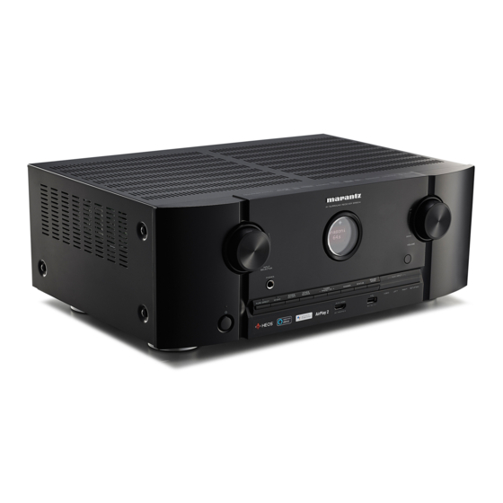
AV Surround Receiver
SR5014
• For purposes of improvement, specifications and design are subject to change without notice.
• Please use this service manual when referring to the operating instructions without fail.
• Some illustrations used in this service manual are slightly different from the actual product.
Service Manual
Click here!
On-line service parts list
http://dmedia.soundunited.com/documents/details/25939
ONLINE PARTS LIST
(P5)
WEB owner's manual
NA:
http://manuals.marantz.com/SR5014/NA/EN/index.php
EU:
http://manuals.marantz.com/SR5014/EU/EN/index.php
AP:
http://manuals.marantz.com/SR5014/AP/ZH/index.php
Upload is planned for the time of a future press release.
BEFORE SERVICING THIS UNIT
ELECTRICAL
MECHANICAL
REPAIR INFORMATION
UPDATING
Confidential
Ver. 1
Advertisement
Table of Contents

Related Manuals for Marantz SR5014


Summary of Contents for Marantz SR5014
- Page 1 Service Manual Ver. 1 AV Surround Receiver SR5014 Click here! On-line service parts list http://dmedia.soundunited.com/documents/details/25939 ONLINE PARTS LIST (P5) WEB owner’s manual http://manuals.marantz.com/SR5014/NA/EN/index.php http://manuals.marantz.com/SR5014/EU/EN/index.php http://manuals.marantz.com/SR5014/AP/ZH/index.php Upload is planned for the time of a future press release. BEFORE SERVICING THIS UNIT...
- Page 2 BEFORE SERVICING THIS UNIT SAFETY PRECAUTIONS NOTE FOR SCHEMATIC DIAGRAM HANDLING THE SEMICONDUCTOR AND OPTICS ONLINE PARTS LIST Accessing the Parts List Searching Part Numbers or Ref. Numbers NOTE FOR PARTS LIST SERIAL NUMBER Serial Number Organization SKU Code of this Unit POST-SERVICE PRECAUTIONS Initializing this Unit JIG FOR SERVICING...
-
Page 3: Safety Precautions
SAFETY PRECAUTIONS The following items should be checked for continued protection of the customer and the service technician. Leakage current check Before returning the set to the customer, be sure to carry out either (1) a leakage current check or (2) a line to chassis resistance check. If the leakage current exceeds 0.5 milliamps, or if the resistance from chassis to either side of the power cord is less than 460 kohms, the set is defective. -
Page 4: Note For Schematic Diagram
NOTE FOR SCHEMATIC DIAGRAM WARNING: Parts indicated by the z mark have critical characteristics. Use ONLY replacement parts recommended by the manufacturer. CAUTION: Before returning the set to the customer, be sure to carry out either (1) a leakage current check or (2) a line to chassis resistance check. -
Page 5: Note For Parts List
On-line service parts list http://dmedia.dmglobal.com/Document/DocumentDetails/XXXXX ONLINE PARTS LIST (P5) WEB owner’s manual http://manuals.marantz.com/AAAAA/NA/EN/index.php http://manuals.marantz.com/AAAAA/EU/EN/index.php http://manuals.marantz.com/AAAAA/AP/ZH/index.php Upload is planned for the time of a future press release. BEFORE SERVICING THIS UNIT NOTE : If the web browser does not open automatically, copy the URL and paste it into the address bar (3) Next, click the "Sheet"... - Page 6 The 14-digit serial number that contains the code of the manufacturing plant and the manufacturing date. 14 digits Factory Manufactured Cumulative Year, month code code serial number The last Month 2digit of year (01 ~ 12) SKU Code of this Unit Product SKU SKU Code SR5014/U1B SR5014/N1B SR5014/N1SG SR5014/K1B...
-
Page 7: Initializing This Unit
POST-SERVICE PRECAUTIONS Initializing this Unit Make sure to initialize this unit after replacing the microcomputer or any peripheral equipment, or the digital PCB. 1. Press the power button to turn off the power. 2. While holding down buttons "TUNER PRESET CH -" and "TUNER PRESET CH +" simultaneously, press the power button to turn on the power. -
Page 8: Schematic Diagrams
ELECTRICAL SCHEMATIC DIAGRAMS PRINTED CIRCUIT BOARDS SCH01 HDMI SW TMDS261B DIGITAL, F HDMI SCH02 HDMI SW1 INPUT, VIDEO, FRONT CNT SCH03 HDMI SW2 SCH04 ADV8003 MAIN, AUDIO IN, RS CNT, GUIDE L, GUIDE SCH05 ADV8003 DDR FRONT, RS232 SCH06 HDMI TX PREOU, USB, HP, SMPS, HDAM SCH07 NET PHY SCH08 CPU... - Page 9 SCHEMATIC DIAGRAMS SCH01 HDMI SW TMDS261B TO 0A HDMI SW FROM HDMI TX TMDS261B R2163 OPEN L1148 CB05YTYH221-2012 L1149 CB05YTYH221-2012 L1146 CB05YTYH221-2012 C2245 2.2U-K-1005 R2156 C2247 1N-K-0603 R2157 OPEN R2158 R2155 ARC_RST R2154 ARC_INT FROM CPU R2152 AVSCL R2153 AVSDA C2211 100N-K-0603 TO 5A...
- Page 10 SCH02 HDMI SW1 HDMI SW1 N1000 N1000 R1026 A111989-A-01-T W/O FLNG RXF_5V Q1006 HP_DET HPD8 RT1N141C Q1007 RT1N441C R1020 DDC_SDA RXF_DDCDA STBY5V FROM R1022 DDC_SCK RXF_DDCCL D.SUPPLY CEC3.3V L1000 CE_REMOTE CEC1.1V1 TXC- L1016 CB05YTYH221-2012 RXF_C- DGND OPEN TO 9A TXC_SHLD TXC+ RXF_C+ TX0-...
- Page 11 SCH03 HDMI SW2 HDMI SW2 N1004 A111989-A-01-T FLNG R1105 RX4_5V HP_DET Q1009 HPD4 RT1N141C DDC_SDA Q1010 FROM RT1N441C DDC_SCK D.SUPPLY R1107 CEC3.3V RX4_DDCDA L1007 CE_REMOTE R1108 CEC1.1V2 RX4_DDCCL TO 4B L1019 CB05YTYH221-2012 TXC- DGND RX4_C- OPEN TXC_SHLD TXC+ RX4_C+ TX0- RX4_0- TX0_SHLD TX0+...
- Page 12 SCH04 ADV8003 ADV8003 CEC3.3V DV5V FROM DV3.3V D.SUPPLY DV1.8V TO 8B DGND AVDD3_1_TX DVDD_TX AVDD3_1_TX AVDD3_1_TX PVDD5_TX DVDDIO_TX L1038 L1042 CB05YTYH101-2012 M21,N21 CB05YTYH221-2012 D20,D21 L1039 A13,B13 CB05YTYH221-2012 TX1_C- TX1_C- PVDD5 AVDD2 PVDD1,2 PVDD3 TX1_C+ TX1_C+ TX1_0- TX1_0- TX1_0+ TX1_0+ TO HDMI TX TX1_1- TX1_1- DDR_1.8V...
- Page 13 SCH05 ADV8003 DDR ADV8003 DDR TO C2 TO C3 TO C4 ADV8003 ADV8003 ADV8003 U1028 A3R12E40DBF-8E(512Mb) U1029 A3R12E40DBF-8E(512Mb) DDR1 DDR2 DDR_1.8V DDR_1.8V DGND DGND DR_TXDQSB1 DDR_1.8V DDR_1.8V DGND DGND DR_TXDQSB3 DDR_1.8V DR_TXDQ14 DGND DR_TXDM1 DR_TXDQS1 DGND DR_TXDQ15 DR_TXDQ30 DGND DR_TXDM3 DR_TXDQS3 DGND DR_TXDQ31...
- Page 14 SCH06 HDMI TX HDMI TX CEC5V_1 CEC5V_1 FROM CEC3.3V D.SUPPLY CEC1.1V N1030 A111989-A-01-T FLNG TO 6C DGND VDD33IO L1115 OPEN-2012 TX2+ P0TX0_2+ L1116 R1984 TX2 SHIELD 0*2(AR) OPEN TX2- P0TX0_2- TX1+ P0TX0_1+ AVDDH33 R1985 L1117 TX1 SHIELD L1082 0*2(AR) OPEN CB05YTYH221-2012 AVDD11 TX1-...
- Page 15 SCH07 NET PHY TO 0D NET PHY TO CPU NET3.3V LEGO5V FROM D.SUPPLY NOT USE NET_I2S2_DOUT P2 TEST Distribution Source or BT TX NET_I2S2_BCKIN P2 TEST Distribution Source or BT TX NET_I2S2_DIN TO 5D NET_I2S2_LRCKIN P2 TEST Distribution Source or BT TX R1297 DGND NET_I2S0_DOUT.
- Page 16 CURRENT DET USB0_DM C1353 100N-K-0603 AMPSIG_DET AMPSIGDET VCC_USB R2182 R1524 MODE AEXP DATA AEXP_DATA 33*4(AR) KEY3 KEY3 174:VREFH0 AEXP CLK AEXP_CLK SR5014/U1B OPEN 175:AVCC0 U1061 U1062 KEY2 KEY2 AEXP OE AEXP_OE 176:NC/COMP_DET CD4094BPWR CD4094BPWR SR5014/N1B OPEN KEY1 KEY1 AEXP STB AEXP_STB...
- Page 17 SCH09 CPU LEVEL CHG CPU LEVEL CHG TO 8E TO DIGITAL CNT FROM REMOTE3.3V SWM3.3V D.SUPPLY M3.3V DGND TO 9E SWM3.3V R1366 DC_PROT R1343 DGND TO CPU TO D9 GND LINE POWER+ LINE POWER- LINE ANALOG AUDIO DIGITAL AUDIO TMDS SIGNAL VIDEO SIGNAL COMPONENT(Y)
- Page 18 SCH10 DSP TO 0F TO 1F TO E1 TO DIR/A.PLD TO CPU N1034 OPEN DSP1CS DSP1MISO DSP1MOSI DSP1CLK DGND DA3.3V L1129 CB05YTYH221-2012 L1130 CB05YTYH221-2012 DSP1MISO DSP1CLK R2181 10K*4(AR) U1023 W9812G6KH-5 C1432 100N-K-0603 R1780 R1775 SD_D0 DQ15 SD_D15 C1435 100N-K-0603 VDDQ VSSQ R1837 DM_DSPOUT_DATA...
- Page 19 SCH11 DIR A.PLD TO A6 TO B3 TO B7 TO C7 TO 2F TO 3F TO D1 TO D4 DIR/A.PLD FROM TMDS261B FROM FROM eARC FROM HDMI SW1 FROM HDMI SW2 HDMI TX MAIN DAC VIDEO PLD FROM NET PHY NET/PHY TO E3 (1) DIR input...
- Page 20 SCH12 MAIN DAC TO F2 TO E5 TO F6 TO F4 TO F7 TO F8 TO E4 TO F5 MAIN DAC FROM FROM FROM FROM FROM FROM DIR/A.PLD DIR/A.PLD DIR/A.PLD DIR/A.PLD DA+5V U1050 MAX : 135mA TLV75733PDBVR D1138 3.3V LRB521S-30 DA+5V C2137 R1999...
- Page 21 SCH13 D.SUPPLY D5V. CEC3.3V M3.3V M3.3V SWM3.3V DA1.0V REMOTE3.3V DV1.8V NET3.3V DA3.3V DV3.3V D.SUPPLY DGND DGND DGND L1054 CB05YTYH221-2012 D5V. L1055 CB05YTYH221-2012 L1056 CB05YTYH221-2012 N1033 HDMI TX L1138 1.5A N1033 TYS50402R2N-10 OPEN-2012 A2505-WV06 6P L1112 CEC1.1V CEC1.1V TO C6 R1812 L1113 OPEN-2012 CEC_POWER...
- Page 22 SCH14 DIGITAL CNT TO G4 DIGITAL CNT TO D.SUPPLY DA+5V C1312 C1311 OPEN-0603 OPEN-0603 N1014 TO CP4201 N1014 C125Z2-27 DAC_FL+ DAC_FL- DAGND DAGND N1029 DAC_FR- OPEN DAC_FR+ DAGND DAGND SLSR_WIRELESS_VDCOM SLSR_WIRELESS_VDCOM CEN+ DAC_C+ DAGND DAGND CEN- DAC_C- WIRELESS_L WIRELESS_L FROM INPUT DAGND DAGND DAGND...
- Page 23 SCH15 VIDEO PLD TO D7 TO D6 TO 6G TO F3 VIDEO PLD FROM NET PHY DIR/A.PLD ADV7180 PO8KI_HSYNC. PO8KI_DE. PO8KI_PCK. PO8KI_VSYNC. PO8KI_Y11/R7. PO8KI_Y10/R6. PO8KI_Y7/R3. PO8KI_Y6/R2. PO8KI_Y9/R5. PO8KI_Y8/R4. PO8KI_Y5/R1. PO8KI_Y4/R0. PO8KI_Y3/G7. LEGOVS DEC_D3. ADV8003 PO8KI_Y2/G6. LEGODE DEC_D2. PO8KI_C11/G3. LEGOVD0 DEC_D1. NETGUI_R0 DEC_D2 PO8KI_C10/G2.
- Page 24 SCH16 ADV7180 ADV7180 L1023 CB C2518T220M L1022 CB C2518T220M L1021 CB05YTYH221-2012 FROM DV1.8V L1020 CB05YTYH221-2012 D.SUPPLY DV3.3V X1019 28.63636MHz(FA-238,7P) DGND C2350 10N-K-0603 C2409 C2406 7P-D-1005 7P-D-1005 C2343 R2251 1K69-F TO G2 82N-K-1005 R2252 OPEN R2250 R2261 R2310 C2345 100N-K-0603 DEC_PCK. DECIN_V.
- Page 25 SCH17 INPUT1 CN4701 CP4200 CP4205 CN4006 CN4703 TO CP4700 TO N1020 TO N1016 TO CP4006 TO CP4007 HDMI_DIGITAL CNT G5 MAIN 3/3 B5 INPUT 1/2 MAIN 2/2 M6 MAIN 2/2 M9 HDMI_DIGITAL CNT M4 INPUT 2/2 TO 7G CN4703 CN4006 C125Z2-09 C125Z2-11 BKT5000...
- Page 26 SCH18 INPUT2 CP4201 INPUT 2/2 TO N1014 HDMI_DIGITAL CNT G3 CP4201 C125Z1-27 BT_TX_L BT_TX_R A_+7V A_+7V A_-7V A_-7V AGND AGND C2138 C2144 OPEN-1608 OPEN-1608 U1049:B A_+7V NJM8080G R2017 C2151 R2018 3K9-F (CH)3900P-J-50V-1608 INPUT 1/2 R2022 R2019 C4239 100/16(KR3) DA_FL_ DA_FL_ DA_FL_ DA_FR_ DA_FR_...
-
Page 27: Video Part
SCH19 VIDEO VIDEO_F/CNT 1/3 VIDEO PART CVBS INPUT SW NJM2595M INPUT OUT PUT SR5014 SW4 SW5 MUTE MUTE VIN 3 CBL/SAT VIDEO_F/CNT 2/3 F4 VIN 4 Blu-ray VIN 2 V.AUX U5001 R5002 NJM2595M CVBS OUT CN5000 Y/V. (Yellow) V+5V V+5V... - Page 28 SCH20 FRONT CNT VIDEO_F/CNT 2/3 FRONT_CNT PART CP3401 HDMI_DIGITAL CNT C4 TO N1039 CP3401 C125Z1-25 CP5000 CP5000 C125Z1-25 F5005A F5005B F5005 T1.25AL 250V TRG_15V_A C5046 OPEN TO CN5000 MAIN TRANS TAP CP5003 F5006 T1.6AL 250V A2505-WR08 F5006A F5006B AC_IN +5V_IN_A VGND VIDEO_F/CNT 1/3 O4 AC_IN...
- Page 29 SCH21 RC5 RS232C VIDEO_F/CNT 3/3 RS232 PART RC-5 PART U4700 PQ120DNA TRG_15V TRIGGER ON/OFF JACK4700 ZD4700 C4704 PJ-308-02(RD) R4722 ZJ16B 100N-K OPEN R5718 C4705 TRG_GND Q5630 100N-K R5719 Q5625 RT1P141C Q5629 RT1P141C RT1N141C C5662 C5663 D4703 LBAS16HT1G OPEN 4700N-K TRG1 C4707 10/50(SK) C4706...
- Page 30 SCH22 AMP1 PAGE 1 7CH_AMP SR5014 AMP SCH 60.7V 60.0V 59.2V R703 D459 R403 R401 R404 1N4148 D473 270(1) R406 OPEN R405 OPEN 270(1) CP501 DHPTF1608-115T C401 D460 C402 100N-K A2001-WR02_2P_2.0MM 1N4148 C404 OPEN C403 R407 D401 1.1V OPEN 0.6V...
- Page 31 SCH23 AMP2 TO G9 PAGE 2 TO H0 PAGE 2 AMP B'D 1/2_A10 PAGE 2 AMP B'D 1/2_M10 R706 R531 R533 D476 R534 R537 270(1) OPEN R535 270(1) OPEN CP504 DHPTF1608-115T D463 C449 C450 1N4148 C452 OPEN A2001-WR02_2P_2.0MM 100N-K D419 OPEN 1N4148 D464...
- Page 32 SCH24 SPK MAIN 1/3 SPK PART 470(2) R4000 H/PR R4016 L4000 SP-2507 RLY4000 D4000 LBAS16HT1G C4000 HFD27/012-S 47N-100V(PEF) C4003 R4002 47N/50V R4003 R4001 470(2) H/PL 10(2) JACK4006 FR_GND C4001 C4002 JXZ-201B(RD,BK) CHASSISGND 2N2/50V OPEN R4017 20(1/5) FR_A L4001 SP-2507 JACK4005 FL_GND JXZ-201B(RD,BK) C4006...
- Page 33 SCH25 TUNER REG SPK PART A8 MAIN 2/3 TO H1 TUNER / REG PART CP4003 VIDEO_F/CNT 2/3 _ J9 A_-7V CP4003 A_+7V C125Z1-19 HDAM_GND HDAM_GND D4010 D4009 H/PL H/P_L 1N4007S 1N4007S TRG_15V TRG_15V H/P_GND H/P_GND CP4002 H/PR H/P_R VIDEO_F/CNT 2/3 _ G9 RLY_F C/S_RL RLY_C/S...
- Page 34 SCH26 RS CNT MAIN 3/3 RS_CNT PART CLP4002 BKT4404 CP4700 INPUT 1/1 C1 TO CN4701 R1452 C1341 OPEN D1094 C1342 4.7U-K-1608 LBAS16HT1G C1343 OPEN U1019 R94EV1A Q1037 CP4700 RT1P141C OUTPUT D1095 C125Z1-15 C1344 BIR-BM1341W 4.7U-K-1608 Z1001 C1345 OPEN SHIELD COVER R1455 R1456 R1467...
- Page 35 R4437 R4439 D/MGND Q4410 R4444 RT1P441C TO N1017 R4449 OPEN D/MGND SR5014 FRONT PANEL KEY LAYOUT PURE DIRECT, M-DAX, ZONE2 ON/OFF, ZONE2 SELECT, PRESET CH-, PRESET CH+, DIMMER, STATUS, SOUND MODE R4477 R4465 R4483 VEC4401 EC16B12SAAD4 ZD4408 C4460 C4465 OPEN...
- Page 36 SCH28 SMPS SR5014 SMPS B'D BKT4140 C4148 0.01UF/250V OPTION OPTION L4140 FC4140B FC4140A SQ2014 27mH D4142 1N4007S F4140 ZD4147 D4143 1N4007S ZJ39B ¡Ü C4143 CP4140 0.22UF/275VAC ZD4148 YW396-03AV ¡Ü D4144 1N4007S ZJ39B ZD4149 D4149 D4145 1N4007S ZJ39B MBR3060PT OPTION OPTION C4149 0.01UF/250V...
- Page 37 SCH29 HDAM HDAM 1/1 CURRENT_FB PART _CN4703 A_-8V R4190 A_-8V R4179 A_-8V KTC3875G R4172 KTA1504S KTA1504S Q4109 R4186 MAIN 3/3 G4 R4185 Q4058 Q4057 Q4059 Q4056 R4236 A_+8V KTA1504S KTA1504S KTC3875G Q4099 KTA1504S A_+8V Q4060 R4349 Q4061 KTA1504S Q4107 KTC3875G OPEN A_+8V R4176...
- Page 38 SCH30 PREOUT PREOUT PART CN5601 C5620 C5629 R5701 CN5601 22/50 22/50 C125Z2-21 R5647 R5665 Q5607 Q5616 OPEN INC2002AC1 R5683 AGND R5638 100K 470K R5648 R5666 OPEN AGND C5651 10N-K AGND Q5617 Q5608 INC2002AC1 OPEN R5684 R5639 AGND 100K 470K R5667 R5649 C5621 C5630...
- Page 39 SCH31 F-HDMI JK201 A111989-G-01-T W/O FLNG HP_DET F.HPD R2003 R2004 10K-1005 10K-1005 DDC_SDA L2001 LBC2012T4R7M DDC_SCK JK202 JK202 CE_REMOTE F.CEC C-A111974-1(V) TXC- TXC_SHLD TXC+ F.HPD HP_DET TX0- F..HDMI5V TX0_SHLD DGND FDGND TX0+ DDC_SDA C2001 F.DDC_SDA TX1- DDC_SCK F.DDC_SCL TX1_SHLD 100N-K-0603 CEC5V TX1+ F.CEC...
- Page 40 PRINTED CIRCUIT BOARDS DIGITAL, F HDMI Lead-free Solder When soldering, use the Lead-free Solder (Sn-Ag-Cu). DIGITAL (A SIDE) F HDMI (A SIDE) F HDMI (A SIDE) JK201 U1056 5M240ZT100C5N SR5014 DIGITAL PCB [MP] N1000 R2133 BKT201 7020-08454-000-0S R2143 U2022 C2402 ADV7180 R2138...
- Page 41 INPUT, VIDEO, FRONT CNT INPUT (A SIDE) INPUT (B SIDE) FRONT CNT (A SIDE) FRONT CNT (B SIDE) R2065 R2064 R2063 R2059 CN4701 R2056 R2055 U1051 R2054 NJM8080G R2052 7P/15P R2048 BKT5001 SR ONLY(17P) R2045 R5072 R2051 R5337 R2050 R5338 BURRING D4215 U4209...
- Page 42 AMP (A SIDE) G403 7CH AMP B'D MM CLAMP 403 CLAMP 402 BAR CODE CP401 WIRE J590 CLAMP 401 7020-08417-000-1S G400 G401 WIRE G401 G402 WIRE C408 BONDING R428 BONDING BONDING R687 R644 JW595 C456 C424 C533 CLAMP 400 R471 C440 R472 C528...
- Page 43 MAIN, AUDIO IN, RS CNT, GUIDE L, GUIDE MAIN (A SIDE) MAIN (B SIDE) AUDIO IN (A SIDE) AUDIO IN (B SIDE) G4200 R4067 C4215 J4150 NJM4580CG U4005 R4063 C4225 C4226 C4223 FILTER OPTION R4073 C4224 - AVR_E2,E1C : BTT87B-01 IC4000 L4201 R4058...
- Page 44 FRONT, RS232 FRONT (A SIDE) FRONT (B SIDE) M3.3V D/MGND SWM3.3V R4448 A+7V A-7V VAUXR AGND C4483 BD4400 VAUXL MICGND C4436 C4482 V.AUX/GND VAUXV H/PGND C4451 H/PL H/PR R4495 FRONT_IRIN SWM5V(MX) POWERKEY REDLED FLCLK D4416 FLDATA FLCE1 D4412 M-DAX_LED R4453 R4459 FLRST R4479...
- Page 45 PREOU, USB, HP, SMPS, HDAM PREOUT (A SIDE) PREOUT (B SIDE) SMPS (A SIDE) SMPS (B SIDE) SMPS B'D MP BKT4140 7020-08415-000-0S C4226 B O N D I N G BKT4141 Sec. CP4140 R4255 Pri. AGND NEUTRAL LIVE AGND AGND AGND FC4141B FC4141A...
-
Page 46: Level Diagram
LEVEL DIAGRAM FRONT ch SR5014 LEVEL DIAGRAM FRONT ch NJU72750 NJU72343 ANALOG H/POUT SPEAKER LINE IN + GAIN ADJ. AK4458VN AK5358B + + PREOUT - - to ZONE2 +30dB NJU72343 MAX. OUTPUT 4.2Vrms SP OUT Differential Out 4.48Vrms/8Ω AK4458 MAX SIGNAL LEVEL... - Page 47 CENTER, SURROUND, SURR.BCK ch SR5014 LEVEL DIAGRAM CENTER ch SURROUND ch SURR.BCK ch NJU72343 SPEAKER + GAIN ADJ. AK4458VN + + PREOUT - - +30dB NJU72343 MAX. OUTPUT 4.2Vrms SP OUT Differential Out 4.23Vrms/8Ω AK4458 MAX SIGNAL LEVEL 0dBFS +20dB DOLBY LIMIT LEVEL (ALLch-3dBFS) 0dBFS = +/-2.8Vpp=1.98Vrms...
- Page 48 SUBWOOFER ch SR5014 LEVEL DIAGRAM SUBWOOFER ch NJU72343 SPEAKER + GAIN ADJ. AK4458VN + + PREOUT - - NJU72343 MAX. OUTPUT 4.2Vrms +30dB MAX SIGNAL LEVEL DOLBY LIMIT LEVEL (ALLch-3dBFS) 0dBFS = +/-2.8Vpp=1.98Vrms AK4458 0dBFS +20dB -10dBFS +10dB PREOUT 300mVrms...
- Page 49 ZONE2 ch (w/ Source) SR5014 LEVEL DIAGRAM Distribution ZONE2(w/ Source) NJU72750 NJU72750 NJU72343 from LINE IN DA SB-ch + SPEAKER GAIN BT_TX PCM5100 AK5358B BD3812(AVR-X2600H、SR5014,NR1710) HEOS + ZONE2 PCM5100 PCM9211 To LEGO +30dB SP OUT 4.70Vrms/8Ω Differential Out MGAIN setting of MASTER VOL 00dB PCM5100 ・SPEAKER OUT(DIGITAL)
- Page 50 ZONE2 ch (w/o Source) SR5014 LEVEL DIAGRAM ZONE2(w/o Source) NJU72750 NJU72750 NJU72343 from LINE IN DA SB-ch + SPEAKER GAIN BT_TX PCM5100 AK5358B BD3812(AVR-X2600H、SR5014,NR1710) HEOS + ZONE2 PCM5100 +30dB SP OUT 4.23Vrms/8Ω MGAIN setting of MASTER VOL 00dB S ・...
-
Page 51: Block Diagram
BLOCK DIAGRAM ANALOG AUDIO DIAGRAM SR5014 ANALOG AUDIO DIAGRAM INVERTING BUFFER H/P-L H/P-R DA_FL DA_FR DA_C DA_SW DA_SL DA_SR DA_SBL DA_SBR (FL-B/FL-H/BI-AMP/ZONE) 7-INPUT/3-OUT (FR-B/FR-H/BI-AMP/ZONE) NJU72750AV 8-CH VOLUME NJU72343 ALL MODEL : FM/AM 7-INPUT/3-OUTPUT InA1 NJU72750 TUNER 8-CH VOLUME InA2 NJU72343... - Page 52 DIGITAL AUDIO DIAGRAM SR5014 DIGITAL AUDIO DIAGRAM TMDS TMDS TMDS OUT0 HDMI OUT2 OUT1 FRONT HDMI SW1_SD0 HDMI OUT1 SW1_SD1 HDMI2.0 TX SW1_SD2 MN864788 HDMI1 HDMI2.0 RX SW1_SD3_SPDIF MN864788 (HDCP 2.2 : 4 INPUTS) SW1_LRCK HDMI2 SW1_BCLK SW1_MCLK HDMI3 HDMI IN...
- Page 53 VIDEO DIAGRAM SR5014 VIDEO DIAGRAM FRONT HDMI TMDS OUTPUT OUT0 HDMI1 HDMI2.0 TX TMDS OUT MN864788 HDMI2.0 RX MN864788 (HDCP 2.2 : 4 INPUTS) TMDS OUT TMDS OUTPUT TMDS OUT HDMI2 W25Q128JVFIQ 4K OSD HDMI3 OUT1 HDMI4 MX25L3206EM2I HDMI5 OUT0...
-
Page 54: Power Diagram
POWER DIAGRAM SR5014 VCC DIAGRAM S1(AMP +B) S2(+8V,-8V) R4032 JUMPER MAIN TRANS R1825 R1800 MAIN PWR ON... -
Page 55: Wiring Diagram
WIRING DIAGRAM SR5014 WIRE DIAGRAM DIGITAL B'D SPK B'D LEGO V4.0 MODULE FRONT CNT B'D VIDEO B'D PREOUT B'D 7CH AMP B'D VOLUME B'D FRONT B'D SELECT B'D H/P B'D USB B'D... - Page 56 DSP(CS49844A) interrupt signal input pin DA3VPu P34/SCK6/SCK0/IRQ4 BDOWN Detect power down M3VPu Pd(S950H/ X2600H) P33/TIOCD0/RXD6/ RC_IN Remote input M3Vpu RXD0/IRQ3-DS (SR5014/ NR1710)" (S950H/X2600H/ P32/TIOCC0/TXD6/ NR1710(EU/JP) Flasher (Remote) input pin (When standby mode,set to inturrupt) -/Pd TXD0/IRQ2-DS FLASHER_IN (NR1710(NA)/SR5014) TMS/NC (NORM- TMS/PF3 E20 Emulator control pin/When normal operating mode,set to input.
- Page 57 MVOL_DATA Volume control pin (NJU72343) USB0_DM USB0_DM NC(open) ZVOL_DATA 113 TRDATA2/PG6 (X2600H/NR1710/ ZONE2 volume control pin (BD3812F) USB0_DP USB0_DP NC(open) SR5014) (S950H) VSS_USB VSS_USB Ground pin ZVOL_CLK 114 PA1/SCK5/IRQ11 (X2600H/NR1710/ ZONE2 volume control pin (BD3812F) AVCC_USBA AVCC_USBA Power supply pin...
- Page 58 Key control signalinput pin (When standby mode,set to inturrupt) M3VPu 172 VREFL0 VREFL0 Ground pin 173 P40 ADC_RST A/D convertor(AK5358) reset control pin 174 VREFH0 VREFH0 Power supply pin 175 AVCC0 AVCC0 Power supply pin COMP_DET 176 P07/IRQ15 Component video signal detect pin (SR5014) (S950H/ M3VPu X2600H/NR1710)
- Page 59 PCM9211 www.ti.com SBAS495 – JUNE 2010 PIN CONFIGURATIONS PCM9211 (DIGITAL : U1040) PT PACKAGE LQFP-48 DESCRIPTION (TOP VIEW) NAME TOLERANT 26 MS/ADR1 Software control I/F, SPI chip select / I2C slave address setting1(2) ERROR/INT0 VDDRX 27 MODE Control mode setting, (see the Serial Control Mode section, NPCM/INT1 RXIN1 MPIO_A0...
- Page 60 PCM9211 CS49844A (DIGITAL : U1073) BLOCK DIAGRAM www.ti.com SBAS495 – JUNE 2010 BLOCK DIAGRAM FILT AUXIN 0 AUTO RXIN7 RXIN 0 RXIN0 SCKO DOUT RXIN 1 RXIN1 MAIN OUTPUT RXIN 2 RXIN2 AUXIN0 LRCK SCKO/ BCK/LRCK PORT RXIN 3 RXIN3 AUXIN1 DOUT RXIN 4/ASCKI 0...
- Page 61 W9812G6KH-5 (DIGITAL : U1023) Block diagram CLOCK BUFFER CONTROL SIGNAL GENERATOR COMMAND DECODER COLUMN DECODER COLUMN DECODER CELL ARRAY CELL ARRAY BANK #0 BANK #1 MODE REGISTER SENSE AMPLIFIER SENSE AMPLIFIER ADDRESS BUFFER Pin description PIN NUMBER PIN NAME FUNCTION DESCRIPTION Multiplexed pins for row and column address.
- Page 62 AK4458VN 40 +105 C (Exposed pad is connected to ground) 40 +85 C (Exposed pad is open) 48-pin QFN (0.5mm pitch) AKD4458 Evaluation Board for AK4458 AK4458VN (DIGITAL : U1051) No. Pin Name I/O Function PD State CAD0_I2C Chip Address 0 Pin in I2C Bus serial control mode Pin Configurations Chip Select Pin in 3-wire serial control mode Hi-Z...
- Page 63 SLAS764 – MAY 2011 www.ti.com [AK4458] DEVICE INFORMATION TERMINAL FUNCTIONS, PCM510x FUNCTIONAL BLOCK DIAGRAM PCM5100A (DIGITAL : U1052, U1054) 4. Block Diagram and Functions PCM510X (top view) LDOE TVDD VDD18 DVSS AVDD AVSS Bias BICK/DCLK DATT AOUTL1P LRCK/DSDL1 Soft Mute Interpolator AOUTL1N SDTI1/DSDR1...
- Page 64 Bipolar Technology Package Outline DIP16,DMP16 PIN CONFIGURATION and BLOCK DIAGRAM NJU72343 (INPUT : U4202) NJM2595MTE1 (VIDEO : U5001) Vin1 Vin2 75Ω Vout1 Driver Vin3 Pin Function 75Ω Vout2 No. Symbol Function No. Symbol Function Vin4 Driver AREF Analog reference potential terminal DATA IC control data input Address selection terminal...
- Page 65 NJM2586AVC3(VIDEO : U5002) 75Ω 75Ω CH1 OUT CH1 OUT CH1 IN1 CH1 IN1 Driver Driver Bias Bias Cont1 Cont1 Cont1 Cont1 Cont2 Cont2 75Ω 75Ω CH2 OUT CH1 IN2 CH1 IN2 CH2 OUT Driver Driver Bias Bias Cont1 Cont1 75Ω CH1 IN3 CH3 OUT 75Ω...
- Page 66 PATTERN DETAIL 2. FL DISPLAY FLD (GP1261AI) (FRONT : FLT4400) 42-1 43-1 44-1 45-1 46-1 47-1 48-1 42-2 43-2 44-2 45-2 46-2 47-2 48-2 42-3 43-3 44-3 45-3 46-3 47-3 48-3 42-4 43-4 44-4 45-4 46-4 47-4 48-4 PIN CONNECTION 42-5 43-5 44-5...
- Page 67 AV Receiver AV Receiver Function description is located right end. RC-5/ RC-5 Ex. Format Command(*7) AV Receiver AV Receiver Made by: Marantz America, LLC. EX/ES 16 37 61 RCRC51603761 Select Dolby EX or DTS-ES Dolby Atmos ON/OFF 16 64 25...
- Page 68 Audyssey Dynamic Volume Mode H 16 28 34 RCRC51602834 Select Audyssey Dynamic Volume mode: Heavy 16 29 16 RCRC51602916 Turn On and select DVD Audyssey Dynamic EQ Offset 0dB 16 28 51 RCRC51602851 MEDIAPLAYER 16 29 17 RCRC51602917 Turn Off Audyssey Dynamic EQ Offset: 0dB Turn On and select VCR1 Audyssey Dynamic EQ Offset -5dB 16 28 52...
- Page 69 TV AUDIO(TV) 16 93 15 RCRC51609315 Turn On and select TV 16 93 16 RCRC51609316 Turn On and select DVD MEDIAPLAYER(VCR1) 16 93 17 RCRC51609317 Turn On and select VCR1 VCR2 16 93 18 RCRC51609318 Turn On and select VCR2 CBL/SAT(SAT) 16 93 19 RCRC51609319...
- Page 70 MECHANICAL DISASSEMBLY Flowchart 1. FRONT ASSY 2. RADIATOR ASSY 3. DIGITAL PCB 4. VIDEO PCB 5. PREOUT PCB 6. MAIN PCB 7. SMPS PCB 8. TRANS EXPLODED VIEW PACKAGING VIEW...
- Page 71 DISASSEMBLY Flowchart • Remove each part following the flow below. • Reassemble the removed parts in the reverse order. • Read "SAFETY PRECAUTIONS" before reassembling the removed parts. • If wire bundles are removed or moved during adjustment or part replacement, reshape the wires after completing the work. Failure to shape the wires correctly may cause problems such as noise. • See "EXPLODED VIEW" TOP COVER FRONT ASSY RADIATOR ASSY DIGITAL PCB DISASSEMBLY DISASSEMBLY DISASSEMBLY 1. FRONT ASSY 2. RADIATOR ASSY 3. DIGITAL PCB and "EXPLODED VIEW" and "EXPLODED VIEW" and "EXPLODED VIEW" HP PCB 7CH_AMP PCB DIGITAL PCB Ref. No. of EXPLODED VIEW : P 1 Ref. No. of EXPLODED VIEW : P 8 Ref. No. of EXPLODED VIEW : P 16 F_HDMI PCB GUIDE L PCB NETWORK MODULE Ref. No. of EXPLODED VIEW : P 2 Ref. No. of EXPLODED VIEW : P 21 Ref. No. of EXPLODED VIEW : P 10 USB PCB Ref. No. of EXPLODED VIEW : P 3 FRONT PCB...
- Page 72 • For the shooting direction of each photos used in this manual, see the photo below. • A, B, C and D in the photo below indicate the shooting directions of photos. Proceeding : TOP COVER → FRONT ASSY • The photographs with no shooting direction indicated were taken from the top of the unit. (1) Remove the screws. • Photos of SR5014 U are used in this manual. The viewpoint of each photograph (Shooting direction : X) [View from the top] ↓Shooting direction: B↓ View from the bottom (2) R emove the screws. Cut the wire clamp, then remove the CORD HOLDER and connector. Remove the FFC. CP4400 ↑Shooting direction: A↑...
-
Page 73: Radiator Assy
2. RADIATOR ASSY 3. DIGITAL PCB Proceeding : TOP COVER → RADIATOR ASSY Proceeding : TOP COVER → DIGITAL PCB (1) Remove the screws. (1) Remove the screws. ↓Shooting direction: D↓ ↓Shooting direction: C↓ View from the bottom ↑Shooting direction: A↑ (2) C ut the wire clamps, then remove the CORD HOLDERs and connectors. Remove the FFC. (2) R emove the screws. Cut the wire clamp, then remove the CORD HOLDER and connector. -
Page 74: Video Pcb
4. VIDEO PCB 6. MAIN PCB Proceeding : TOP COVER → DIGITAL PCB → VIDEO PCB Proceeding : TOP COVER → DIGITAL PCB → VIDEO PCB → PREOUT PCB → PREOUT PCB (1) Remove the connector. (1) Remove the screws. CN5000 View from the bottom (2) Remove the screws. Remove the connector. -
Page 75: Exploded View
3 X2 C X2 45 X2 1 X2 C X6 20X2 23 X4 O X2 22 X4 WARNING: E X8 SR5014 ALL Parts marked with this symbol z have critical characteristics. Use ONLY replacement parts recommended by the manufacturer. P X4... - Page 76 PACKAGING VIEW http://dmedia.soundunited.com/documents/details/25939 Parts List : ZIPPERBAG(A5size) ZIPPERBAG(A4size) SETUP MIC STAND SIZE : 350mm x 210mm EU toll-free leaflet (Mz) (N only) Notes on RADIO (ALL) This part together with document and zipper bag are supplied. SPOTIFY insertion sheet (U/N) Cautions on Using Batteries (N Only) MIC STAND ASSEMBLY INSTRUCTIONS QUICK START GUIDE ( ALL )
-
Page 77: Troubleshooting
REPAIR INFORMATION TROUBLE SHOOTING SPECIAL MODE 1. POWER Special mode setting button 2. Analog video 1. Version Display Mode 3. HDMI/DVI 2. PANEL / REMOTE LOCK Selection Mode 4. AUDIO 3-1. Selecting the Mode for Service-related 5. Network / Bluetooth / USB 3-2. - Page 78 TROUBLE SHOOTING 1. POWER 1.1. The unit does not power on 1.2. Fuse is blown The unit does not power on Blown fuse Check for short circuits between the Does the power indicator on the front panel flash Check the rectifier diode in the Does the power shut down after several seconds? Check for leaks and short circuits regulator output terminal and GND...
-
Page 79: Analog Video
DIGITAL PCB Check the connection between the boards. : [R2141] DIGITAL test point COMPONENT-Y : [R2138] COMPONENT-Cb : [R2140] U1056 COMPONENT-Cr : [R2139] 5M240ZT100C5N SR5014 DIGITAL PCB [MP] N1000 R2133 7020-08454-000-0S R2143 R2138, R2139, U2022 C2402 ADV7180 R2138 N1017 N1019... - Page 80 Input Input CVBS COMPONENT Check the settings of each IC. Check the settings of each IC. Are the following voltages set? Are the following voltages set? DIGITAL PCB DIGITAL PCB faulty. DIGITAL PCB DIGITAL PCB faulty. [N1039 : 12pin] : Hi (3.3 V) [N1039 : 11pin] : Lo (0 V) [N1039 : 13pin]...
- Page 81 3.1. No picture or sound is output (HDMI to HDMI) No picture or sound is output. (8) When using a MARANTZ Blu-ray/DVD player, is the "HDMI" indicator of the fluorescent display lit? Proceed to YES when using a Blu-ray/DVD player produced by other manufactures.
- Page 82 (15) Are a picture and sound output when a differ- The TV is faulty. ent TV is used? Check the unit. "HDMI "Rx/Tx" Failure Detection"...
- Page 83 4. AUDIO 4.1. AUDIO CHECK No audio output CHECK 1 INPUT SURROUND MODE SOURCE Check the ANALOG AUDIO BLOCK Audio output OK? ANALOG 2CH DIRECT ANALOG CHECK 2 INPUT SURROUND MODE SOURCE Check the DIGITAL AUDIO BLOCK Legacy Audio output OK? COAX or OPT (PCM or DolbyDigital or dts…) CHECK 3...
-
Page 84: Analog Audio
4.2. Power AMP (AMP PCB) 4.3. Analog audio When using the protection pass mode, do not connect speakers to the speaker terminals. No audio output. No audio output. Protection is activated. Is a voltage of ± 7V supplied to INPUT PCB Repair the ±... -
Page 85: Cannot Connect To The Network
5. Network / Bluetooth / USB 5.1. Cannot connect to the network Check the connection environment The circuit of NET5V POWER Insert the LAN cable correctly and then turn on Can the output voltage (5V) to Is NET5V POWER [U1018 : 48pin Is the LAN cable correctly inserted? between [U1018-U1080 : FET- the power again. - Page 86 5.2. Cannot establish a Bluetooth connection Check the Bluetooth device being used Are the versions of the HEOS Version displayed in The Network Module software is faulty. Version Check Mode? Is the Bluetooth device compatible with the A2DP Use a device that is A2DP profile compatible. profile? The circuit of Network Module is faulty.
- Page 87 5.3. Cannot recognize the connected USB device 5.4. No picture or sound is output Check the USB device being used Checking the unit (If no picture is output) Are digital video signals(LEGOPCK, LEGOVS, The circuit around Network Module, [U1056 : Is a USB hub being used? Do not use a USB hub.
- Page 88 DIGITAL test point USB test point CN4402 U1056 5M240ZT100C5N SR5014 DIGITAL PCB [MP] N1000 R2133 7020-08454-000-0S R2143 U2022 C2402 ADV7180 R2138 N1017 N1019 C4463 C1292 C2248 R1373 TOP FACE TOUCH AREA C2256 R2144 BKT1001 R1360 C1295 Q1022 U1056 R2309 R2139...
- Page 89 6. SMPS Operation waveform for each part DC 5V is not output. After primary side rectification Primary drain (Caution: High voltage, electric shock) (Caution: High voltage, electric shock) Replace the [U4140 : TOP268VG C4148 0.01UF/250V OPTION Is [U4140 : TOP268VG] dam- OPTION and D4142 / D4143 / D4144 / D4142...
- Page 90 AUDIO CHECK PATH : Digital Signal : Analog Signal HDMI BLOCK CHECK6 HDMI HDMI SPEAKER OUTPUT HDMI INPUT OUTPUT CHECK5 INPUT PREOUT HDMI Transceiver CHECK4 AVR Supported "HD AUDIO" OUTPUT HDMI Transceiver MN864788 ARC INPUT MN864788 FRONT HDMI INPUT Digital audio BLOCK I2S/HBR AUDIO SPDIF COAXIAL...
- Page 91 HDMI "Rx/Tx" Failure Detection 1. Prior checking Check item(1.). : Checking the HDMI connector Checking the condition of the HDMI pin (rear/front). There are deformed pins. Replace the HDMI connector. Check for deformed pins. None of the pins are deformed. Check by following the flow chart for "3.
- Page 92 2. Preparations for checking HDMI Switcher reception/transmission register 2-3. Device configuration method 2-1. Necessary devices PC settings : Execute the serial communication program, Termite.exe. Check the product settings. 2-a) Player with an HDMI terminal After executing Termite.exe, click [Settings]. 2-b) TV with an HDMI terminal (* NOTE : Do not use a computer monitor.) Windows PC Serial communication software "Termite.exe"...
- Page 93 Click the [click to connect] button to start communication. When the settings are correct, the following message will be displayed in the window of Termite. After a connection is established successfully, the display of the button name will change as shown in [00]Start Sub CPU Log Mode Figure 4.
- Page 94 3. Starting detecting the point of failure Check item(3.1.). Display when an Error is not detected. Check the power supply status and communication status with the CPU of each device. L1 1 Auto Start in HDMI Diagnostics mode and follow the procedures below. Test Start in HDMI Diagnostics mode Cancel the mode, and proceed to...
- Page 95 Check item(3.2.). : Check operation of the HDMI input terminal. Check item(3.4). : Check operation of the HDMI output termi- nal. Go to check item (3-14.1.). (GUI IC [ADV8003] failure detection When the HDMI input terminal of this device is connected to the player correctly, is sound heard from procedure 2 the speaker? ※...
- Page 96 3-1. Error Code H1-01 failure detection procedure Checking device. [U1039 : MN864788] Check the power supply voltage. (HDMI Tx) Checking the reset waveform. (HDMI Tx) Check item(3-1.1.). Check the power supply voltage. : Check item(3-1.3.). Checking the reset waveform : Check the waveform.
- Page 97 Check the I2C communication line. (HDMI Tx) Check item(3-1.4.). Check the I2C communication line : Check the CPU. Is the "I2C" waveform of the TP near the HDMI Tx [U1039] correct (like the one shown in the diagram) when the power is turned on? HSDA Check item(3-1.5.).
- Page 98 3-2. Error Code H1-02 failure detection procedure Checking device. [U1000 : MN864788] Check the power supply voltage. (HDMI Rx) Checking the reset waveform. (HDMI Rx) Check item(3-2.1.). Check the power supply voltage. : Check item(3-2.3.). Checking the reset waveform : Check the waveform.
- Page 99 Check the I2C communication line. (HDMI Rx) Check item(3-2.4.). Check the I2C communication line : Check the CPU. Is the "I2C" waveform of the TP near the HDMI Rx [U1000] correct (like the one shown in the diagram) when the power is turned on? HSCL HSDA...
- Page 100 3-3. Error Code H1-03 failure detection procedure Checking device. [U1003 : MN864788] Check the power supply voltage. (HDMI Rx) Checking the reset waveform. (HDMI Rx) Check item(3-3.1.). Check the power supply voltage. : Check item(3-3.3.). Checking the reset waveform : Check the waveform.
- Page 101 Check the I2C communication line. (HDMI Rx) Check item(3-3.4.). Check the I2C communication line : Check the CPU. Is the "I2C" waveform of the TP near the HDMI Rx [U1000] correct (like the one shown in the diagram) when the power is turned on? HSCL HSDA...
- Page 102 3-4. Error Code H1-06 failure detection procedure Checking device. [U1026 : ADV8003] Check the power supply voltage. Checking the reset waveform. Check item(3-4.1.). Check the power supply volt- Check item(3-4.2.). Check the power supply volt- Check item(3-4.3.). Checking the reset : age.
- Page 103 Check the I2C communication line. Check item(3-4.4.). Check the I2C communication line : Check the CPU. Is the "I2C" waveform of the TP near the CPU [U1018] correct (like the one shown in the diagram) when the power is turned on? U1018 AVSDA AVSCL *The diagram shows an example.
- Page 104 3-5. Error Code H1-14 failure detection procedure 3-6. Error Code H1-15 failure detection procedure Checking device. [U1028, U1029 : A3R12E40DBF-8E] Checking device. [U1027 : W25Q128JVFIQ] Check item(3-6.1.). Check item(3-5.1.). Write to the GUI ROM. Check soldering of IP SCALER [U1026], DDR2 [U1028/U1029] and its peripheral circuits. Check soldering of the resistors [R1688/1689/1692/1695 to 1700/1703 to 1711] between IP SCALER and...
- Page 105 3-7. Error Code H1-04 failure detection procedure 3-8. Error Code H1-05 failure detection procedure Checking device. [U1103 : TMDS261B] Checking device. [U2022 : ADV7180] Check item(3-7.1.). Check item(3-8.1.). Replace [U1103] with a new device. Replace [U2022] with a new device. Recheck from check item (3.1.).
- Page 106 3-9. Error Code H1-08 failure detection procedure Checking device. [U1073 : CS49844A] Check the power supply voltage. Checking the reset waveform. Check item(3-9.1.). Check the power supply volt- Check item(3-9.2.). Check the power supply volt- Check item(3-9.3.). Checking the reset : age.
- Page 107 Check the SPI communication line. Check item(3-9.4.). Check the SPI communication line : Check the CPU. Is the "SPI" waveform of the TP near the DSP [U1073] correct (like the one shown in the diagram) when the power is turned on? 3pin CLK 4pin MODI 6pin CS...
- Page 108 3-10. Error Code H1-12 failure detection procedure Checking device. [U1040 : PCM9211] Check the power supply voltage. Checking the reset waveform. Check item(3-10.1.). Check the power supply volt- Check item(3-10.2.). Check the power supply volt- Check item(3-10.3.). Checking the reset : age.
- Page 109 Check the communication line. Check item(3-10.4.). Check the communication line : Check the CPU. Is the waveform of the TP near the DIR [U1040] correct (like the one shown in the diagram) when the power is turned on? DIR_CLK U1040 DIR_DIN DIR_CE DIR_DOUT...
- Page 110 3-11. Error Code H1-16 failure detection procedure Checking device. [U1009 : Sil9437] Check the power supply voltage. (ARC IC) Checking the reset waveform. (ARC IC) Check item(3-11.1.). Check the power supply voltage. : Check item(3-11.3.). Checking the reset waveform : Check the waveform.
- Page 111 Check the I2C communication line. (ARC IC) Check item(3-11.4.). Check the I2C communication line : Check the CPU. Is the waveform of the TP near the ARC IC [U1009] correct (like the one shown in the diagram) when the power is turned on? AVSCL R5152 AVSDA R2153 U1009...
- Page 112 3-12. HDMI Rx [MN864788] failure detection procedure Checking operation between the HDMI (Rx) device and the player Check item(3-12.2.). Checking the DDC status register : Example Send the following command from Termite.exe. HDMI Rx1 (When checking HDMI inputs 1, 2, and 3) b In order to check, connect the player to the HDMI terminal and configure the player as AVR source.
- Page 113 When the results of check item (3-12.1.) are "00" When the results of check item (3-12.2.) are "00 or 04" (Detection of 5V is not OK) (Detection of DDC is not OK.) Check the +5V voltage. (HDMI Rx) Check the DDC line. (HDMI Rx) Check item(3-12.3.).
- Page 114 When the results of check item (3-12.2.) are "22" (Detection of DDC is OK.) Checking the TMDS status register 3.3V TMDS Signal TMDS Check item(3-12.5.). Checking register of the TMDS CLK detection sta- Example tus register : Example of waveform in check ① Example of waveform in check ② Send the following command from Termite.exe.
- Page 115 3-13. HDMI DDC Buffer failure IC detection procedure Checking operation between the HDMI (HDMI DDC Buffer) and the player Checking the +5V/DDC status register (HDMI DDC Buffer) Check item(3-13.3.). Checking the 5V status of the register : Example Send the following command from Termite.exe. b In order to check, connect the player to the HDMI terminal and configure the player as AVR source.
- Page 116 When the results of check item (3-13.3.) are "00" When the results of check item (3-13.4.) are "00 or 04" (Detection of 5V is not OK.) (If the DDC are not OK) Check the +5V voltage. (HDMI DDC Buffer) Check the DDC line. (HDMI DDC Buffer) less than 100KHz Check item(3-13.5.).
- Page 117 When the results of check item (3-13.4.) are "22" (Detection of DDC is OK) Checking the TMDS status register Check item(3-13.7.). Check the TMDS CLK detection status of the Check item(3-13.8.). Checking the TMDS input waveform. : Example 3.3V TMDS Signal register : : Check the TMDS waveform at the following test point.
- Page 118 3-14. HDMI transmission IC [MN864788] failure detection procedure Check the output terminal. Check item(3-14.1.). Check the video output port for failure. : Check the Monitor 1 output video signal is correct. After checking the Monitor 1, change the HDMI cable connection from OUT1 to OUT2. Turn off the AV AMP and turn it on again.
- Page 119 When the results of check item (3-14.1.) are "No video signal is output from both Monitor 1 and Monitor Checking between Monitor1 and the TV. 2". Connect Monitor1 to the TV and check the following items with the TV turned on. Checking operation between the HDMI (Rx) device and the HDMI device (Tx).
- Page 120 Example When the results of check item (3-14.4.) are "30" (Detection of HPD is OK / Detection of RXSENSE is OK ) Checking the EDID register. (Monitor1) Check item(3-14.5.). Check the Monitor EDID : ① Unplug the AC cord. Plug the AC cord into a power outlet. The first eight bytes are nor- ②...
- Page 121 When the results of check item (3-14.4.) are "10" When the results of check item (3-14.4.) are "20" (Detection of HPD is OK / Detection of RXSENSE is not OK ) (Detection of HPD is not OK / Detection of RXSENSE is OK ) Check the RXSENSE.
- Page 122 When the results of check item (3-14.4.) are "00" Checking between Monitor 2 and the TV. (Detection of HPD is not OK / Detection of RXSENSE is not OK ) Connect Monitor2 to the TV and check the following items with the TV turned on. Check the RXSENSE/HPD.
- Page 123 When the results of check item (3-14.11.) are "03" (Detection of HPD is OK / Detection of RXSENSE is OK ) Example Checking the EDID register. (Monitor2) Check item(3-14.12.). Check the Monitor EDID : ① Unplug the AC cord. Plug the AC cord into a power outlet. ②...
- Page 124 When the results of check item (3-14.11.) are "01" When the results of check item (3-14.11.) are "02" (Detection of HPD is OK / Detection of RXSENSE is not OK ) (Detection of HPD is not OK / Detection of RXSENSE is OK ) Check the RXSENSE.
- Page 125 When the results of check item (3-14.11.) are "00" (Detection of HPD is not OK / Detection of RXSENSE is not OK ) Checking the HPD/RXSENSE status register. (Monitor2) Check item(3-14.17.). Checking the HPD and RXSENSE. : Does the test point of RXSENSE close to the HDMI output terminal [N1030] indicate the (3.3V)? Does the voltage of HPD test point close to the HDMI output terminal [N1030] indicate Hi (3-5 V)?
- Page 126 3-15. GUI IC [ADV8003] failure detection procedure Checking the TMDS status register (GUI -> HDMI Tx) Check item(3-15.1.). Check the TMDS CLK detection status of the Example register. Send the following command from Termite.exe. Send the command "i 0006 00FF 0001".
- Page 127 3-16. HDMI SW IC [TMDS261B] failure detection procedure Checking the TMDS status register (HDMI SW -> GUI) Example Check item(3-16.1.). Check the TMDS CLK detection status of the register. Send the following command from Termite.exe. Send the command "i 00E2 0004 0001".
- Page 128 4. Device implementation location DIGITAL (A SIDE) F-HDMI (A SIDE) JK201 U1056 R1692, R1695,R1696,R1697, 5M240ZT100C5N SR5014 DIGITAL PCB [MP] N1000 R2133 BKT201 R1698,R1699,R1700,R1703, 7020-08454-000-0S R2143 U2022 C2402 N1019 ADV7180 R2138 N1000 N1017 C1292 R1704,R1705,R1706,R1707,R1710, C2248 TOP FACE TOUCH AREA R2144...
-
Page 129: Clock Flow & Wave Form In Digital Block
U2403 SCLK PLDADCBCK AK5358B ANALOG Rch LRCK PLDADCLRCK SDTO PLDADCDATA (2)DIROUT I2S (3) DAC input (9)DACIN I2S U1056 5M240ZT100C5N SR5014 DIGITAL PCB [MP] N1000 R2133 7020-08454-000-0S R2143 U2022 C2402 ADV7180 R2138 N1017 N1019 C1292 C2248 TOP FACE TOUCH AREA R2144... -
Page 130: Special Mode Setting Button
SPECIAL MODE Special mode setting button b No. 1 - 4, 6 - 8 : While holding down buttons "A", "B" and "C" simultaneously, press the power button to turn on the power. b No. 5, 9, 10 : While the power is on, hold down buttons "A", "B", and "C" for at least 3 seconds . Mode Button A Button B Button C Descriptions... - Page 131 @@@@@@ \ A.PLD SN%%%*** Config Audy IF ******** ******** Producti @ : Model name (SR5014) **.** \ : Region (U, N, K, F) y Video PLD : % : SKU code Q3 HEOS Locale : V.PLD w Firmware Package :...
- Page 132 1.4. Error display See the table below for descriptions of the displayed errors and countermeasures for these. If multiple errors occur, only one item is displayed. The priority order is w, e, r, t, y, q. Condition States Display TROUBLE SHOOTING The model name, brand name and region information written in the firmware are compared L1 FIRM to the region settings in the PCB.
- Page 133 Condition States Display TROUBLE SHOOTING L1 DSP Boot error 1 (After reset the DSP, DSP_Flag0 port is "Low") ERROR Boot Error 2 (After reset the DSP, MCU received state error command) Signal Detect Error (No response after input set for 1sec) Mode Change Error (No response after mode change for 1sec) •...
- Page 134 1.5. Version Display in the Setup Menu Follow the steps below to display the firmware information. (1) Press the "SETUP" button on the remote control. (2) Select "General - Information - Firmware". The version information is displayed as a 16-digit number as shown in the screenshot below. General/Firmware Version XXXX-XXXX-XXXX-XXXX...
- Page 135 2. PANEL / REMOTE LOCK Selection Mode 2.1. Actions Switch the PANEL LOCK and REMOTE LOCK modes between on and off. RC LOCK • PANEL LOCK Mode (with Volume) Disables reception from all keys and encoders on the front panel except the power button (including the volume).
- Page 136 3-1. Selecting the Mode for Service-related 3-1.1. Actions Select diagnostic mode (service path check mode), protection history display mode, 232C standby clear 4OP INFO mode, Operation Info mode or TUNER STEP mode. 3-1.2. Starting up While holding down buttons "ZONE2 SOURCE" and "STATUS" simultaneously, press the power button Operation Info for the unit can be checked.
-
Page 137: Protection History Display Mode
3-2. Protection History Display Mode 3-2.1. Actions (3) DC (if the last protection is DC) This mode enables the unit to record and display the event when the THERMAL, ASO or DC protection is activated. Cause : DC output of the power amplifier is abnormal. If protections have been activated multiple times, the latest protection operation is recorded. - Page 138 3-2.4. Clearing the Protection History 3-3. 232C Standby Clear Mode There are two ways to clear the protection history. 3-3.1. Actions (1) Activate Protection History Display Mode. Press the "STATUS" button to display the protection Switches from 232C standby mode to normal standby mode. history.
- Page 139 3-4. Operation Info Mode 3-4.1. Actions (3) DC / ASO Protection count This mode enables the unit to display the accumulated operating time, power On count and each Protect protection count. DC:____ 3-4.2. Starting up ASO:___ While holding down buttons "ZONE2 SOURCE" and "STATUS" simultaneously, press the power button to turn on the power.
- Page 140 3-5. TUNER STEP mode (U / N only) 3-5.1. Actions This is a special mode that enables the reception frequency STEP of the ANALOG TUNER to be changed. 3-5.2. Starting up While holding down buttons "ZONE2 SOURCE" and "STATUS" simultaneously, press the power button to turn on the power.
-
Page 141: Network Initialization Mode
4. Protection Pass Mode 5. Network Initialization Mode 4.1. Actions 5.1. Actions • This mode allows the power to be turned on without activating protections. The following items are initialized. • This mode functions in the same way as normal power-on, except that protections are not activated. Network setup •... - Page 142 6. Clearing of Operation Info 7. Log Capture feature 6.1. Actions 7.1. Actions • Displays the accumulated operating time of the unit, the number of times the power was switched • Acquires the Network Module log. on, and the number of occurrences of each protection. •...
- Page 143 DIAGNOSTIC MODE Service Path Check Mode 1.1. Actions This function is convenient for confirming problem paths in the product and checking the paths after repairing. The Video and Audio paths can be checked. The backup data is not rewritten. 1.2. Starting up While holding down buttons "ZONE2 SOURCE"...
- Page 144 Paths to be confirmed Display Settings What to confirm Input Source : HEOS Music • Digital(PCM) input ⇒ Speaker output (Surround Back (ZONE2) L/R) Input Mode : Auto • Digital(PCM) input ⇒ Pre OUT output (ZONE2 L/R) Sound mode : STEREO ( b Only HEOS Music can be set as the input source.) DIGITAL fig.A03a...
- Page 145 1.6. Confirmation items for the video system See the block diagram fig.VXXth. Paths to be confirmed Display Settings What to confirm Input Source : CBL/SAT • CVBS input ⇒ CVBS output Video Convert : Off (IP Scaler : Off), All sources •...
-
Page 146: Diagnostic Path Diagram
DIAGNOSTIC PATH DIAGRAM fig.A01 SR5014 ANALOG AUDIO DIAGRAM INVERTING BUFFER H/P-L INVERTING BUFFER (OPEN) (OPEN) H/P-R DA_FL DA_FR DA_C DA_SW DA_SL DA_SR DA_SBL DA_SBR (FL-B/FL-H/BI-AMP/ZONE) 7-INPUT/3-OUT (FR-B/FR-H/BI-AMP/ZONE) NJU72750AV 8-CH VOLUME NJU72343 ALL MODEL : FM/AM 7-INPUT/3-OUTPUT InA1 NJU72750 TUNER 8-CH VOLUME... - Page 147 SR5014 DIGITAL AUDIO DIAGRAM TMDS TMDS TMDS OUT0 HDMI OUT2 OUT1 FRONT HDMI SW1_SD0 HDMI OUT1 SW1_SD1 HDMI2.0 TX SW1_SD2 MN864788 HDMI1 HDMI2.0 RX MN864788 SW1_SD3_SPDIF (HDCP 2.2 : 4 INPUTS) SW1_LRCK HDMI2 SW1_BCLK SW1_MCLK HDMI3 HDMI IN TMDS...
- Page 148 SR5014 ANALOG AUDIO DIAGRAM INVERTING BUFFER H/P-L H/P-R DA_FL DA_FR DA_C DA_SW DA_SL DA_SR DA_SBL DA_SBR (FL-B/FL-H/BI-AMP/ZONE) 7-INPUT/3-OUT (FR-B/FR-H/BI-AMP/ZONE) NJU72750AV 8-CH VOLUME NJU72343 ALL MODEL : FM/AM 7-INPUT/3-OUTPUT InA1 NJU72750 TUNER 8-CH VOLUME InA2 NJU72343 InA3 OutA1 MAIN_AD_IN_L MAIN_L...
- Page 149 SR5014 DIGITAL AUDIO DIAGRAM TMDS TMDS TMDS OUT0 HDMI OUT2 OUT1 FRONT HDMI SW1_SD0 HDMI OUT1 SW1_SD1 HDMI2.0 TX SW1_SD2 MN864788 HDMI1 HDMI2.0 RX MN864788 SW1_SD3_SPDIF (HDCP 2.2 : 4 INPUTS) SW1_LRCK HDMI2 SW1_BCLK SW1_MCLK HDMI3 HDMI IN TMDS...
- Page 150 SR5014 ANALOG AUDIO DIAGRAM INVERTING BUFFER H/P-L H/P-R DA_FL DA_FR DA_C DA_SW DA_SL DA_SR DA_SBL DA_SBR (FL-B/FL-H/BI-AMP/ZONE) 7-INPUT/3-OUT (FR-B/FR-H/BI-AMP/ZONE) NJU72750AV 8-CH VOLUME NJU72343 ALL MODEL : FM/AM 7-INPUT/3-OUTPUT InA1 NJU72750 TUNER 8-CH VOLUME InA2 NJU72343 InA3 OutA1 MAIN_AD_IN_L MAIN_L...
- Page 151 SR5014 DIGITAL AUDIO DIAGRAM TMDS TMDS TMDS OUT0 HDMI OUT2 OUT1 FRONT HDMI SW1_SD0 HDMI OUT1 SW1_SD1 HDMI2.0 TX SW1_SD2 MN864788 HDMI1 HDMI2.0 RX MN864788 SW1_SD3_SPDIF (HDCP 2.2 : 4 INPUTS) SW1_LRCK HDMI2 SW1_BCLK SW1_MCLK HDMI3 HDMI IN TMDS...
- Page 152 SR5014 ANALOG AUDIO DIAGRAM INVERTING BUFFER H/P-L H/P-R DA_FL DA_FR DA_C DA_SW DA_SL DA_SR DA_SBL DA_SBR (FL-B/FL-H/BI-AMP/ZONE) 7-INPUT/3-OUT (FR-B/FR-H/BI-AMP/ZONE) NJU72750AV 8-CH VOLUME NJU72343 ALL MODEL : FM/AM 7-INPUT/3-OUTPUT InA1 NJU72750 TUNER 8-CH VOLUME InA2 NJU72343 InA3 OutA1 MAIN_AD_IN_L MAIN_L...
- Page 153 SR5014 DIGITAL AUDIO DIAGRAM TMDS TMDS TMDS OUT0 HDMI OUT2 OUT1 FRONT HDMI SW1_SD0 HDMI OUT1 SW1_SD1 HDMI2.0 TX SW1_SD2 MN864788 HDMI1 HDMI2.0 RX MN864788 SW1_SD3_SPDIF (HDCP 2.2 : 4 INPUTS) SW1_LRCK HDMI2 SW1_BCLK SW1_MCLK HDMI3 HDMI IN TMDS...
- Page 154 SR5014 ANALOG AUDIO DIAGRAM INVERTING BUFFER H/P-L H/P-R DA_FL DA_FR DA_C DA_SW DA_SL DA_SR DA_SBL DA_SBR (FL-B/FL-H/BI-AMP/ZONE) 7-INPUT/3-OUT (FR-B/FR-H/BI-AMP/ZONE) NJU72750AV 8-CH VOLUME NJU72343 ALL MODEL : FM/AM 7-INPUT/3-OUTPUT InA1 NJU72750 TUNER 8-CH VOLUME InA2 NJU72343 InA3 OutA1 MAIN_AD_IN_L MAIN_L...
- Page 155 SR5014 ANALOG AUDIO DIAGRAM INVERTING BUFFER H/P-L H/P-R DA_FL DA_FR DA_C DA_SW DA_SL DA_SR DA_SBL DA_SBR (FL-B/FL-H/BI-AMP/ZONE) 7-INPUT/3-OUT (FR-B/FR-H/BI-AMP/ZONE) NJU72750AV 8-CH VOLUME NJU72343 ALL MODEL : FM/AM 7-INPUT/3-OUTPUT InA1 NJU72750 TUNER 8-CH VOLUME InA2 NJU72343 InA3 OutA1 MAIN_AD_IN_L MAIN_L...
- Page 156 SR5014 DIGITAL AUDIO DIAGRAM TMDS TMDS TMDS OUT0 HDMI OUT2 OUT1 FRONT HDMI SW1_SD0 HDMI OUT1 SW1_SD1 HDMI2.0 TX SW1_SD2 MN864788 HDMI1 HDMI2.0 RX MN864788 SW1_SD3_SPDIF (HDCP 2.2 : 4 INPUTS) SW1_LRCK HDMI2 SW1_BCLK SW1_MCLK HDMI3 HDMI IN TMDS...
- Page 157 SR5014 ANALOG AUDIO DIAGRAM INVERTING BUFFER H/P-L H/P-R DA_FL DA_FR DA_C DA_SW DA_SL DA_SR DA_SBL DA_SBR (FL-B/FL-H/BI-AMP/ZONE) 7-INPUT/3-OUT (FR-B/FR-H/BI-AMP/ZONE) NJU72750AV 8-CH VOLUME NJU72343 ALL MODEL : FM/AM 7-INPUT/3-OUTPUT InA1 NJU72750 TUNER 8-CH VOLUME InA2 NJU72343 InA3 OutA1 MAIN_AD_IN_L MAIN_L...
- Page 158 SR5014 VIDEO DIAGRAM FRONT HDMI TMDS OUTPUT OUT0 HDMI1 HDMI2.0 TX TMDS OUT MN864788 HDMI2.0 RX MN864788 (HDCP 2.2 : 4 INPUTS) TMDS OUTPUT TMDS OUT TMDS OUT HDMI2 W25Q128JVFIQ 4K OSD HDMI3 OUT1 HDMI4 MX25L3206EM2I HDMI5 OUT0 HDMI SWITCH...
- Page 159 SR5014 VIDEO DIAGRAM FRONT HDMI TMDS OUTPUT OUT0 HDMI1 HDMI2.0 TX TMDS OUT MN864788 HDMI2.0 RX MN864788 (HDCP 2.2 : 4 INPUTS) TMDS OUTPUT TMDS OUT TMDS OUT HDMI2 W25Q128JVFIQ 4K OSD HDMI3 OUT1 HDMI4 MX25L3206EM2I HDMI5 OUT0 HDMI SWITCH...
- Page 160 SR5014 VIDEO DIAGRAM FRONT HDMI TMDS OUTPUT OUT0 HDMI1 HDMI2.0 TX TMDS OUT MN864788 HDMI2.0 RX MN864788 (HDCP 2.2 : 4 INPUTS) TMDS OUTPUT TMDS OUT TMDS OUT HDMI2 W25Q128JVFIQ 4K OSD HDMI3 OUT1 HDMI4 MX25L3206EM2I HDMI5 OUT0 HDMI SWITCH...
- Page 161 SR5014 VIDEO DIAGRAM FRONT HDMI TMDS OUTPUT OUT0 HDMI1 HDMI2.0 TX TMDS OUT MN864788 HDMI2.0 RX MN864788 (HDCP 2.2 : 4 INPUTS) TMDS OUTPUT TMDS OUT TMDS OUT HDMI2 W25Q128JVFIQ 4K OSD HDMI3 OUT1 HDMI4 MX25L3206EM2I HDMI5 OUT0 HDMI SWITCH...
- Page 162 SR5014 DIGITAL AUDIO DIAGRAM TMDS TMDS TMDS OUT0 HDMI OUT2 OUT1 FRONT HDMI SW1_SD0 HDMI OUT1 SW1_SD1 HDMI2.0 TX SW1_SD2 MN864788 HDMI1 HDMI2.0 RX MN864788 SW1_SD3_SPDIF (HDCP 2.2 : 4 INPUTS) SW1_LRCK HDMI2 SW1_BCLK SW1_MCLK HDMI3 HDMI IN TMDS...
- Page 163 SR5014 ANALOG AUDIO DIAGRAM INVERTING BUFFER H/P-L H/P-R DA_FL DA_FR DA_C DA_SW DA_SL DA_SR DA_SBL DA_SBR (FL-B/FL-H/BI-AMP/ZONE) 7-INPUT/3-OUT (FR-B/FR-H/BI-AMP/ZONE) NJU72750AV 8-CH VOLUME NJU72343 ALL MODEL : FM/AM 7-INPUT/3-OUTPUT InA1 NJU72750 TUNER 8-CH VOLUME InA2 NJU72343 InA3 OutA1 MAIN_AD_IN_L MAIN_L...
- Page 164 SR5014 DIGITAL AUDIO DIAGRAM TMDS TMDS TMDS OUT0 HDMI OUT2 OUT1 FRONT HDMI SW1_SD0 HDMI OUT1 SW1_SD1 HDMI2.0 TX SW1_SD2 MN864788 HDMI1 HDMI2.0 RX MN864788 SW1_SD3_SPDIF (HDCP 2.2 : 4 INPUTS) SW1_LRCK HDMI2 SW1_BCLK SW1_MCLK HDMI3 HDMI IN TMDS...
- Page 165 SR5014 VIDEO DIAGRAM FRONT HDMI TMDS OUTPUT OUT0 HDMI1 HDMI2.0 TX TMDS OUT MN864788 HDMI2.0 RX MN864788 (HDCP 2.2 : 4 INPUTS) TMDS OUTPUT TMDS OUT TMDS OUT HDMI2 W25Q128JVFIQ 4K OSD HDMI3 OUT1 HDMI4 MX25L3206EM2I HDMI5 OUT0 HDMI SWITCH...
-
Page 166: Jig For Servicing
JIG FOR SERVICING Use the following jigs (extension cable kit) when repairing the PCBs. Order with your dealer for the jigs your dealer if necessary. CN5000 CAUTION : Incorrect connections may cause malfunction. Connection of Jig for DIGITAL PCB ---Items to Be Prepared--- 8U-110084S : EXTENSION UNIT KIT 1 Set 8U-110136S : EXTENSION UNIT KIT... - Page 167 (4) Connect the expansion cables. Board-to-Board Connections Ref. No. Ref. No. FRONT CNT N1020 DIGITAL 21pin CP4200 INPUT 31pin CP4205 INPUT N1016 DIGITAL 27pin CP4201 INPUT N1014 DIGITAL 25pin CP3403 FRONT CNT N1039 DIGITAL 11pin CP4204 INPUT CN5003 VIDEO 25pin CP5000 FRONT CNT CN5000...
-
Page 168: Adjustment Procedure
ADJUSTMENT Adjusting Idling Current NOTE: Adjusting the idling current when "ECO Mode" is set may damage the Power AMP. 1. Preparation (1) Prepare a DC voltmeter. AMP UNIT (2) Place the unit under normal usage conditions, away from highly ventilated areas such as next to an air conditioning machine or electric fan. - Page 169 UPDATING PROCEDURE AFTER REPLACING THE PCB. PROCEDURE AFTER REPLACING THE U-COM, ETC. FIRMWARE UPDATE PROCEDURE 1. Items necessary for update 2. Update preparation with a USB flash drive 3. Update method when the DIGITAL PCB or network module is replaced (Using a USB flash drive) 4.
- Page 170 (2) Be sure to replace the software with the latest version. DIGITAL U1041 5M570ZF256C5N SOFTWARE : AUDIO PLD U1056 5M240ZT100C5N DIGITAL U1055 5M240ZT100C5N SOFTWARE : VIDEO PLD SR5014 DIGITAL PCB [MP] N1000 R2133 7020-08454-000-0S R2143 U2022 C2402 R2138 N1017 N1019...
-
Page 171: Firmware Update Procedure
Update download file when the firmware is updated (Two files, "HW component" and "LEGO component") Download from SDI Model Name Model Area For HW component For LEGO component SR5014 U North America (U) Product ID : 100100760100 SR5014 N Europe (N) Product ID : 100100760200 DPMS_SR5014ALL_LEGO_xxxx.zip... - Page 172 2. Update preparation with a USB flash drive You can update the firmware by downloading the latest version with USB flash drive. 2.1. Connecting to the USB flash drive (1) Preparation • Windows PC • USB flash drive format : Prepare a USB flash drive formatted in FAT16 or FAT32. b We recommend a USB flash drive that has an LED installed.
- Page 173 3. Update method when the DIGITAL PCB or network module is replaced (Using a USB flash drive) 3.1. File structure on USB flash drive (5) USB Update starts automatically. The Standby LED lights red. DIGITAL PCB or network module is replaced onto the USB flash drive in the following structure. Display during USB update (Main Display) L1 Wait After unzipping the files, store them in the root of the same USB flash drive.
- Page 174 4. Update Method for Service Region Settings Copy the Service Region Settings from the USB flash drive to this unit. (5) Copy the files created on the USB flash drive. 4.1. Creating a Service Region Settings file (1) Click [Start button] - [Accessories] - [notepad] on the PC to launch the notepad. copy to USB flash drive (2) Enter "TEXT".
- Page 175 5. Normal Firmware Update Method from USB Flash Drive 5.1. File structure on USB flash drive (1) Press the power button to turn on the power. (2) Wait for this unit to start up. Copy the normal update files onto the USB flash drive in the following structure. (3) Set the input source to HEOS Music.
-
Page 176: Network Connection
6. Normal Firmware Update Method from OTA 6.2. Check and update the firmware Download the latest firmware from our website and update the firmware. Check if there is a firmware update available. It is also possible to check approximately how long the ---Cautions on Firmware Update--- update will take. - Page 177 Display(Main Display) General L1 Updating Main CPU L2 ––– Main FBL (No used) DSP1 or DSP **min DSP2 ↓ b Except : NR1510/NR1510/SR5014/SR6014 L1 Error DSP3 Update ErrorYYXX : DeviceID, : ErrorCode) YYXX b Except : NR1510/NR1510/SR5014/SR6014 L3 Please check you DSP4 L3 : Content of the display is scrolled.
- Page 178 Copyright © 2019 D&M Holdings Inc. All Rights Reserved.