Furuno FS-1570 Service Manual
Ssb radio telephone
Hide thumbs
Also See for FS-1570:
- Operator's manual (222 pages) ,
- Installation manual (92 pages) ,
- Specifications (2 pages)
Table of Contents
Advertisement
Quick Links
Advertisement
Table of Contents

Related Manuals for Furuno FS-1570


Summary of Contents for Furuno FS-1570
- Page 1 SSB Radio telephone FS-1570/2570...
- Page 2 All rights reserved. Printed in Japan Printed in Japan PUB.No. PUB.No. SME-56360-A SME-56360-A ( ( NAYO NAYO ) ) FS-1570/2570 FS-1570/2570 *SME56360A00* *SME56360A00* *SME56360A00* *SME56360A00* * S M E 5 6 3 6 0 A 0 0 * * S M E 5 6 3 6 0 A 0 0 *...
-
Page 3: Table Of Contents
Contents Check List ........................i Chapter 1. General 1.1 General...........................1-1 1.2 Configuration of System....................1-2 1.2.1 FS-1570 (150W) .....................1-2 1.2.2 FS-2570 (250W) .....................1-3 1.3 Connection of NBDP terminal, IB-581 .................1-4 1.4 Port Specification ......................1-5 1.5 Handset ..........................1-6 1.6 Communication priority ....................1-6 1.7 Display of Receiving DSC message ................1-7 1.8 Power Status Monitor, PSM-01..................1-8... - Page 4 Contents Chapter 3. Set up 3.1 MMSI Number, Model and Group ID ................3-1 3.1.1 MMSI Number (MMSI CLEAR)..............3-1 3.1.2 Model (ALL CLEAR) ..................3-2 3.1.3 Group ID ......................3-3 3.2 RT SETUP ........................3-4 1. NB (ON/OFF).....................3-6 2. SQ FREQ. (500 Hz-2000 Hz)..............3-6 3.
- Page 5 2. T-CPU (FS-1570T/FS-2570T) Program number; 0550205-01.xx ....4-13 3. DSC MODEM (DSC DSP board) Program number; 0550207-01.xx..4-14 4. NBDP MODEM (NBDP DSP board) Program number; 0550208-01.xx ...4-14 5. IB-583 (FS-1570/FS-2570 NBDP terminal) Program number; 0550209-22.xx.....................4-14 6. IB-581 (FS-1570/FS-2570 NBDP terminal) Program number;...
- Page 6 Contents Chapter 5. Block Description 5.1 Configuration.........................5-1 5.1.1 Transceiver unit ....................5-1 5.1.2 Boards in Transceiver unit ................5-3 5.1.3 Control unit, FS-2570C...................5-5 5.1.4 NBDP Terminal unit: IB-581/583 (Option) ............5-6 5.1.5 Antenna coupler unit..................5-8 5.2 Power supply unit ......................5-9 5.2.1 General......................5-9 5.2.2 RELAY board (05P0744)................5-10 5.2.3 SW REG board (05P0737) ................5-10 5.3 T-CPU board (05P0732)....................5-11 5.3.1 Function of CPU .....................5-12...
- Page 7 Contents 5.8 Antenna coupler, AT-1560.....................5-46 5.8.1 Antenna tuning....................5-52 5.9 IB-583 ..........................5-57 5.9.1 TERM CPU board (16P0209A)..............5-58 5.9.2 PWR Board (16P0211A) ................5-59 Chapter 6. Maintenance 6.1 Self-test..........................6-1 6.1.1 DSC test ......................6-1 6.1.2 RT test ......................6-5 6.2 Self test of Antenna coupler ..................6-10 6.3 Self-test of Terminal Unit ....................6-11 6.4 Tone test.........................6-13 6.5 TEST function in DSC SETUP menu ................6-15...
- Page 8 Contents Appendix 1) DSC Frequency List ................AP1-1 Appendix 2) DSC and NBDP Test Calls ..............AP2-1 AP2.1 DSC Test Call ....................AP2-1 AP2.2 NBDP test .....................AP2-3 AP2.2.1 Receiving MSI (Maritime safety Information) ........AP2-3 AP2.2.2 ARQ communication ................AP2-5 Appendix 3) Cancelling and receiving distress alert..........AP3-1 AP3.1 Cancelling distress alert................AP3-1 AP3.2 ........................AP3-1 Appendix 4) Specifications..................AP4-1...
-
Page 9: Check List
Check List 1. Check of installation The cable must be fixed firmly and tidy. Item to be checked Result Refer to Do you understand the system configuration? Chapter 1 Mounting and wiring of transceiver, controller and power supply unit - All securing screws are fully tightened. - Units are grounded. - Page 10 Page 3-1 Check registered MMSI in DSC Setup display. Page 3-27 Model, FS-1570 or FS-2570 is selected through the menu. Power Page 3-2 data and contents of RT self test differ between two models. The RT is set through Setup menu.
- Page 11 Check List DIP switch setting on T-CPU board The default setting is screened. Function C. Loop (IEC: Pos.) (DMC) (MIF) (N.C) RS-422 RS-232C RS-422 IC-303-DSC S4, S5 IC-xxx DMC-5 S6, S7 IC-302-DSC DSC System setup menu The default setting is screened. Items to be set Value INTERNAL...
- Page 12 Check List RT System setup menu The default setting is screened. Menu Setting SQ FREQ 500Hz to 2000Hz (800Hz) FAX RX ENABLE OFFHOOKED SPKER SYSTEM Password is needed to set following items. REGULATION INTL TX FREQ FREE MARINE ITU/USER USER RX FREQ FREE MARINE...
- Page 13 Press [3 TEST] with DSC display. Page 6-1 Press [3 TEST] with RT display. Items to be RT self test checked differ between FS-1570 Page 6-5 FS-2570. Terminal unit self [F6], select “self test” Page 6-11 test Set S2#2 to ON and press [S3:TUNE] on the Antenna coupler COUP board.
- Page 14 Check List Test result Program Program Version MAIN (T-CPU) Transceiver unit DSC modem NBDP modem No.1 FS-2570C: PANEL-1 (C-CPU) Controller unit No.1 FS-2570C: PANEL-2 (C-CPU) IB-581 Terminal unit NBDP terminal IB-583 Terminal unit AT-1570 5. Functional check Item to be checked Result Refer to Position from GNSS is displayed in DSC display.
- Page 15 Check List Transmitter check list Meter indication Power TUNE Freq. Error Frequency Output data OK/NG (within +10Hz) J3E: J2B: J3E: J2B: J3E: J2B: J3E: J2B: J3E: J2B: J3E: J2B: J3E: J2B: J3E: J2B: J3E: J2B: J3E: J2B: 6. Communication test See Appendix 2.
- Page 16 Check List 7. Noise and interference check list Following checks are made in all bands to make sure that no interference to and from the radiotelephone is observed. During transmission (voice and TLX), check that; Result The distress alert and the incoming indicator are not interfered. *LED brightness does not change and the buzzer sounds without noise.
- Page 17 Check List Interference from FS-1570/2570 Band Inmarsat B Inmarsat C No.1 VHF No.2 VHF No.1 radar No.2 radar No.1 GPS No.2 GPS NAVTEX Amplifier Sounder Gyro Steering panel...
-
Page 18: Chapter 1. General
Chapter 1. General 1.1 General FS-1570 (150W) and FS-2570 (250W) are a MF/HF radiotelephone with built-in DSC, DSC watch receiver and NBDP. 1) Two controllers, FS-2570Cx2 can be connected to the transceiver unit: [CONTROLLER-1] (high priority) and [CONTROLLER-2] ports. The system is turned on and off only by the controller 1. -
Page 19: Configuration Of System
1.2 Configuration of System 1.2 Configuration of System 1.2.1 FS-1570 (150W) Fig.1.2.1 shows the configuration of FS-1570. Fig.1.2.1 Configuration of FS-1570... -
Page 20: Fs-2570 (250W)
1.2 Configuration of System 1.2.2 FS-2570 (250W) Fig.1.2.2 shows the configuration of FS-2570. Note)DSC general frequencies watch receiver antenna; 1) Install a DSC watch receiver antenna (FAX-5+2.6 m Whip), or 2) Use MF/HF antenna. When the antenna is used commonly, SSB and NBDP cannot be used during the scanning of DSC general frequencies. -
Page 21: Connection Of Nbdp Terminal, Ib-581
The NBDP terminal IB-581 can be connected to the system by using IF-8500, instead of IB-583 as below. IB-581 and IB-583 use a different NBDP terminal program. IB-581 for FS-1570/2570 differs from one for DP-6 terminal program . Fig.1.3.1 Connection of IB-581... -
Page 22: Port Specification
IEC61162-1 RS-422/C.Loop (NMEA Ver.2.0 GGA>RMC>GLL, ZDA) DMC or DIP SW selectable: S6 and S7 TB-8 RS-422/C.Loop Distress Button on T-CPU board FS-1570: 20 A TB-1, 2 24VDC FS-2570: 35 A MAIN UNIT RS-485 NBDP RS-232C SD, RD PRINTER* Centronics For DSC and NBDP Type: HS-2001 MIC)600Ω, –10dBm... -
Page 23: Handset
1.5 Handset 1.5 Handset Either HANSET (HS2001) port or HANDSET/MIC (HSC-701K-20B) port is used. Do not use them at the same time. HOOK and PTT lines of these ports are connected in parallel. Fig.1.5.1 Block diagram of C-IF HOOK signal: - AUTO ACK of DSC does not work when the handset is off-hooked. -
Page 24: Display Of Receiving Dsc Message
1.7 Display of Receiving DSC message 1.7 Display of Receiving DSC message The received DSC message is displayed depending on the priority. In the distress alert message display, the safety message received is not displayed, but printed out. When the messages in the same category are received, the latest message is displayed and printed. -
Page 25: Power Status Monitor, Psm-01
1.8 Power Status Monitor, PSM-01 1.8 Power Status Monitor, PSM-01 The power status monitor, PSM-01 is optionally available. The unit generates aural and visual alarms when the ship’s supply is switched from the ship’s mains to the reserve source. The unit is installed at the place where the ship is normally navigated. Fig.1.8.1 Connection of PMS-01 1.9 Using NBDP When using the NBDP, taking into account the followings. -
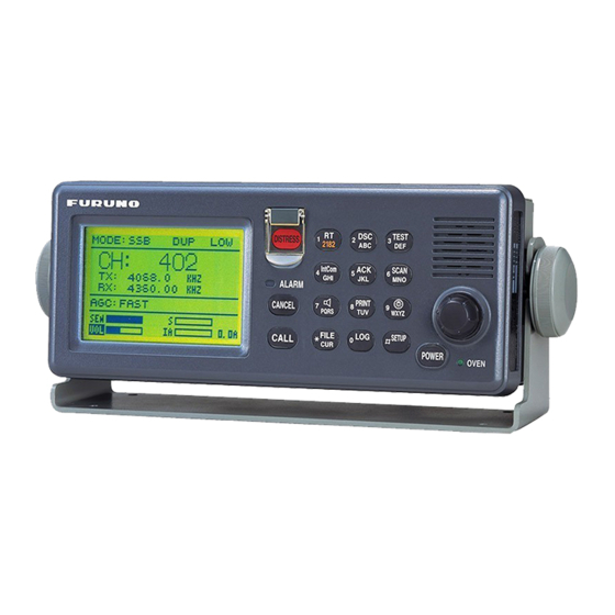
Page 26: Chapter 2. Location Of Parts
Chapter 2. Location of Parts 2.1 FS-2570C Loudspeaker (120 x 64 dots) (1 W or more, External loudspeaker has high priority.) Knob (For moving cursor and using as ENT key) OVEN (When the unit is on, the lamp lights.) Fig.2.1.1 Display unit, front view NBDP: External loudspeaker Connected to [DTE] of IB-583, or... - Page 27 2.1 FS-2570C Fig.2.1.3 Display unit cover C-IF (05P0730) J8: GND J4: NBDP J6: HANDSET-1 J2: MAIN UNIT J5: HANDSET-2/MIC J7: SP/KEY J3: PRINTER (KEY:Not used) AF PA: U7 (TA7252AP) Fig.2.1.4 C-IF (05P0730) board, side A - Display unit with cover removed LINE OUT GAIN ADJ.
- Page 28 2.1 FS-2570C U4: MBM29F800TA U10: M38881M2 (8 Mbit Flash ROM) U16: 15V to 5V (Printer CONT) S1: NMI SW power supply (Not used) U9: GATE ARRY (KEY/LCD CONT) U6, U7: SRAM (128 kx8) U5: EEPROM U3: MPU (MB91101PF) (AT28C256-20PC) CR2: Not used Socket type CR1: Not used Fig.2.1.6 C-CPU (05P0729) board, side A...
- Page 29 2.1 FS-2570C Fig.2.1.8 Display unit with C-CPU (05P0729) board removed Fig.2.1.9 PANEL board (05P0728), side - Display unit with shield cover removed Loudspeaker Ω /0.5 W) Fig.2.1.10 PANEL (05P0728) board side A (above) and Panel with loudspeaker (below)
-
Page 30: Fs-2570T
2.2 FS-2570T 2.2 FS-2570T Cooling fan (Operates when the temperature rises to 45 °C.) Temperature sensor for cooling fun Front view Side view Fig.2.2.1 Transceiver unit REMOTE Cable inlet (MODEM, RT program update port) Connected to AT-1560 Connected to DSC Distress/safety watch receiver antenna CONTROLLER-2 CONTROLLER-1... - Page 31 2.2 FS-2570T Shield cover Shield covers Fig.2.2.3 Transceiver unit with door opened PRESEL (05P0746) SW-REG (05P0737) RELAY (05P0744) DRV (05P0738) W/R2 (05P0734) W/R1 (05P0734) PA (05P0739) REF OSC (05P0747) COMB (05P0740) TX-RX (05P0733) CPU (05P0732) TX-FIL (05P0736) T-IF (05P0731) DSP (05P0751) DSP (05P0751) (For NBDP) (For DSC)
- Page 32 2.2 FS-2570T SW-REG (05P0737) R20: Adjusting +15V DRV (05P0738) R25: DRV PA BIAS ADJ. (100 mA) PA (05P0739) R33: PA IC ADJ. R26: VC ADJ. R16: PA BIAS ADJ. (200 mA) TX-FIL (05P0736) R76: ALC Power adjustment Fig.2.2.5 Back side of the transceiver door...
- Page 33 2.2 FS-2570T W/R (05P0734) J3: When FAX-5 antenna is connected, select ACTIV side. (Short circuit between 1 and 2.) TX/RX (05P0733) R320: RX IF GAIN ADJ. W/R2 R214: H3E carrier ADJ. W/R1 R209: TX IF GAIN ADJ. 18 MHz Ref. OSC ADJ. T-CPU (05P0732) S1: NMI SW DIP SW (S4, S5)
-
Page 34: Fs-1570T
2.3 FS-1570T 2.3 FS-1570T Cooling fan (Operates when the Temperature temperature rises to 45 °C) sensor for cooling fan Front view Side view Fig.2.3.1 Transceiver unit REMOTE Cable inlet (MODEM and RT program update port) Connected to AT-1560 Connected to DSC distress/safety CONTROLLER-2 CONTROLLER-1 watch receiver antenna... - Page 35 2.3 FS-1570T Shield cover Shield covers Fig.2.3.3 Transceiver unit with door opened PRESEL (05P0746) RELAY (05P0744) W/R1 (05P0734) SW-REG (05P0737) REF OSC (05P0747) PA (05P0735) TX-RX (05P0733) CPU (05P0732) TX-FIL (05P0736) T-IF (05P0731) DSP (05P0751) DSP (05P0751) (For DSC) (For NBDP) Fig.2.3.4 Transceiver unit with shield covers removed 2-10...
- Page 36 2.3 FS-1570T SW-REG (05P0737) R20: Adjusting +15V PA (05P0735) R37: VC ADJ. R33: PA IC ADJ. R25: PA BIAS ADJ. (200 mA) TX-FIL (05P0736) R76:ALC Power adjusting Fig.2.3.5 Backside of the transceiver door 2-11...
- Page 37 2.3 FS-1570T W/R (05P0734) J3: When FAX-5 antenna is connected, select ACTIV. (Short circuit between 1and 2.) W/R1 TX/RX (05P0733) R320: RX IF GAIN ADJ. R214: H3E carrier ADJ. R209: TX IF GAIN ADJ. 18 MHz Ref. OSC ADJ. T-CPU (05P0732) S1: NMI SW DIP SW (S4, S5) DIP SW (S2, S3)
-
Page 38: Boards In Transceiver Unit
TX/RX (05P0733) R6: RX RF (Q3, 4) BIAS ADJ. (F+72.455 kHz) 6MHz DDS 3Lo(455 kHz) R320: RX IF GAIN ADJ. R214: H3E carrier ADJ. R209: TX IF GAIN ADJ REF OSC (05P0747) 18MHz ADJ. Fig.2.4.1 TX/RX (05P0733) board, FS-1570/2570 2-13... - Page 39 U5: EEPROM S1: NMI SW (Socket type) DSP (05P0751) U39: +5V REG DIP SW: S4 DIP SW: S5 DIP SW: S3 DIP SW: S7 DIP SW: S2 DIP SW: S6 C69: 1F (U29 RTC backup) Fig.2.4.2 CPU (05P0732) board, FS-1570/2570 2-14...
- Page 40 JP3: When FAX-5 antenna is connected, select ACTIV. (Short circuit between 1 and 2.) (F+54.455 kHz) 6 MHz DDS 3Lo(455 kHz) Fig.2.4.3 W/R 1, 2 (05P0734) board, FS-1570/2570 R37: VC ADJ. (To adjust BAIS, cut L4 and connect an ammeter.) J3: PA OUT J2: PA IN R25: PA BIAS ADJ.
- Page 41 2.4 Boards in Transceiver Unit L4: To adjust BAIS, cut L4 and connect R26: VC ADJ. an ammeter. J3: PA OUT J2: PA IN R33: PA IC ADJ. R16: PA BIAS ADJ. (200 mA) Fig.2.4.5 PA (05P0739) board, FS-2570 R25: DRV PA BIAS ADJ.
- Page 42 J9: DIV OUT 1 J2: TX IN J10: DIV OUT 2 R76: ALC Power adjusting Note: For FS-2570, when the transmission and receiving antenna is connected to W/R2, short circuit JP1, and cut JP2. TX ANT Fig.2.4.8 TX-FIL (05P0736) board, FS-1570/2570 2-17...
- Page 43 TP1-TP2 Used to measure oscillation frequency. (220kHz+20kHz) C13: 220 pF (For oscillation frequency) R20: Adjusting +15V Fig.2.4.9 SW-REG (05P0737) board, FS-1570/2570 RT2 (Polyswitch soldered to opposite side on production sets): 900 mA PA 24 V (-) PA 24 V (+)
- Page 44 (Connected to No.1 FS-2570C) RCV BZ: #9-#16 CONTROLLER-2 EXT BK: #17-#21 (Connected to No.2 FS-2570C) IEC-61162: #22-#26 DMC: #27-#32 Note: No.1 FS-2570C has high priority . (The system power is turned on/off only by No.1 control unit.) Fig.2.4.11 T-IF (05P0731) board, FS-1570/2570 2-19...
-
Page 45: Antenna Coupler
2.5 Antenna coupler 2.5 Antenna coupler These wires should not Leed relay touch any parts. (Selecting either L8 or L9.) Arrester COUP board (05P0528A) Matching Indicator Dummy Ω +250 pF:200 W) Matching Indicator Dummy board (05P0610) Clamp for coaxial cable S1 [AUTO/MANUAL] (Clamp the coaxial Tuning mode selector... - Page 46 2.5 Antenna coupler Figure below shows the difference between AT-1560-25 and –15. AT-1560-25: Leed relay used COUP board (05P0528) Dummy Ω +250 pF:100 W) Dummy board (05P0543) Fig.2.5.2 Antenna coupler, AT-1560-15 (For 150 W) 2-21...
- Page 47 2.5 Antenna coupler THROUH LED lights when “Dummy ON/OFF” LED lights when matching circuit is bypassed. dummy is connected. TUNE LED lights during tuning LED for CPU RUN (Blinking normally) S4, S5 and S6: DIP SW R63: Ia ADJ. used to adjust 2182 kHz with S1 set to MANUAL.
- Page 48 2.5 Antenna coupler Wires should not touch any parts. These carry high tension. See note. Adjust the arrester for about 2 mm gap. Fig.2.5.4 Parts around antenna terminal Danger Note; High voltage presents at the antenna terminal and associated parts. If the wires touch the parts, leaking will Electrical Shock result.
-
Page 49: Terminal Unit, Ib-583
2.6 Terminal unit, IB-583 2.6 Terminal unit, IB-583 JUNCTION (Not provided on IB-583) PRINTER KEYBOARD LAN (Not provided on IB-583) 24 VDC power connecter Power switch (For 2HD disk) Fig.2.6.1 Terminal unit, Front and rear views Fig.2.6.2 Dimensions 2-24... - Page 50 2.6 Terminal unit, IB-583 JUNCTION (Not provided on IB-583 ) PRINTER TERM CPU (16P0209A) PWR (16P0211A) J6 (See note 1.) J9 (See note 2.) PWR C (16P0214) FDD (JU-226A032FCK2149) FDD connecter (See note 3.) Fig.2.6.3 Terminal unit with cover removed Note 1) Disconnecting flat cable from J6 To disconnect the flat cable, gently, set the locking tab to vertical position and then pull out the cable from the connector.
- Page 51 2.6 Terminal unit, IB-583 Note 2) Disconnecting flat cable from J9 To disconnect the flat cable; 1. Release the locking tabs by pushing the tabs toward the cable about 1 mm gently. Excess force will damage the connector. 2. Pull out the cable. To connect the cable, reverse the above procedure.
- Page 52 2.6 Terminal unit, IB-583 Panel SW (16P0212) LCD unit (LCD: NL6448BC33-46) Fig.2.6.7 Panel with LCD unit removed 2-27...
-
Page 53: Boards In Terminal Unit
2.6 Terminal unit, IB-583 2.6.1 Boards in Terminal Unit Not provided on IB-583 PRINTER JUNCTION S1, S2, S3 (from left) S1:CPU reset S2:ULTRA I/O reset S3:Q2I reset S4: DIP SW JP1 (To disconnect the battery) CPU RUN Blinking Lithium battery every second S5: DIP SW (Not provided... - Page 54 2.6 Terminal unit, IB-583 Fig.2.6.9 PWR (16P0211A) board Not used Buzzer Power switch (Distress button for FELCOM) Fig.2.6.10 SW (16P0212) board 2-29...
-
Page 55: Handset (Hs-2001)
2.7 Handset (HS-2001) 2.7 Handset (HS-2001) PTT switch Fig.2.7.1 Handset, HS-2001 ON/OFF hook detecting magnet Fig.2.7.2 Handset hunger 2-30... - Page 56 2.7 Handset (HS-2001) U5 (Hole element) (ON/OFF hook detector) HS board (05P0745) Ear speaker Condenser microphone Fig.2.7.3 Handset Fig.2.7.4 HS board (05P0745), parts side 2-31...
-
Page 57: Chapter 3. Set Up
Chapter 3. Set up The radiotelephone and the DSC are set up through “RT SETUP” and “DSC SETUP“ menus respectively. Either No.1 controller or No.2 controller can be used for setting up. The DIP switch on T-CPU board is set according to the system configuration. -
Page 58: Model (All Clear)
2. Enter password ([x][x][x][x][x][x]). 3. Move the cursor to ”ALL CLEAR” and then press [ENT]. 4. Select the model and then press [ENT]. Difference between FS-1570 and FS-2570 is the contents of the self-test menu and default power data 5. -
Page 59: Group Id
3.1 MMSI Number, Model and Group ID 3.1.3 Group ID The group ID is registered for up to 150 groups from DSC setup menu. 1. Press [SETUP] on DSC display. 2. Move the cursor over “MESSAGE” and then press [ENT]. “Message File entry” appears. -
Page 60: Rt Setup
3.2 RT SETUP 3.2 RT SETUP The RT is set up through RT SETUP menu as below. 1. Press [SETUP] in RT display. “Setup menu” appears. 2. Select the item by the dial key. To show “SYSTEM” menu, the password is needed. 3. - Page 61 3.2 RT SETUP Table 3.2.1 lists the RT Set up menu. Table 3.2.1 RT Set up menu Item Option Remarks SQ FREQ 500 Hz to 2000 Hz (800 Hz) FAX RX ENABLE Displayed when “USER CH” in USER CH See page 3-11. SYSTEM menu is set to ON.
-
Page 62: Nb (On/Off)
3.2 RT SETUP 1. NB (ON/OFF) The noise blanker (NB) is set to ON or OFF. The noise blanker, U15 on TX/RX board (05P0466) reduces pulse noise. In J2B (DSC and NBDP) and J3C (FAX) modes, the noise blanker is automatically set to OFF and no indication appears on the display. 2. -
Page 63: Offhook Spker (On/Off)
3.2 RT SETUP 5. OFFHOOK SPKER (ON/OFF) The ON/OFF Hook of the handset is detected and the speaker is set to ON/OFF by this setting. The table below shows the speaker on/off setting based on “OFFHOOKED SPKER” setting and the handset condition. OFFHOOKED SPKER setting Handset Speaker... -
Page 64: Tx Freq. (Free, Marine/User, Itu/User)
3.2 RT SETUP 7. TX FREQ. (FREE, MARINE/USER, ITU/USER) The transmission frequency is registered. FREE TX frequency is selected in the range from 1.605 MHz to 27.5 MHz and typed in before transmission. The emission mode is selectable for each frequency. The registered USER CH and ITU channel are also used to set the transmission frequency. -
Page 65: User Ch (On/Off)
3.2 RT SETUP 9. USER CH (ON/OFF) When USER CH is set to ON, “USER CH” is registered and erased. When USER CH is set to OFF, “USER CH” is not displayed in RT SETUP menu. 10. AM ENABLE (ON, TRX, RX) AM (H3E) mode is switched on or off. -
Page 66: Coupler Throu (Off, Rcvd, Diff)
3.2 RT SETUP 13. COUPLER THROU (OFF, RCVD, DIFF) The receiving signal can bypass the tuning circuit in the antenna coupler. The signal received by the antenna is sent to the transceiver unit through the tuning circuit in the antenna coupler. RCVD The received signal bypasses the tuning circuit in the antenna coupler. -
Page 67: User Ch Registration
3.2 RT SETUP 3.2.1 USER CH Registration A maximum of 255 user channels are registered for radiotelephone, NBDP and DSC calls. The user channels are available in the following menus. · Compose Message · “MESSAGE” in DSC SET UP menu ·... -
Page 68: Erasing All User Channels
3.2 RT SETUP The following is the pop-up window which appears for frequency selection when creating a message file in “Message file entry” menu. The user channels are grouped into the same band. OTHER can contain four user channels of 0 band. Any frequency is set on the user channel of 0 band of which mode is DSC only. -
Page 69: Erasing User Channel Individually
3.2 RT SETUP 3.2.3 Erasing user channel individually To erase a user channel; 1. Press [SETUP] in RT display. 2. Select “USER CH” in RT SETUP menu and then press [ENT]. 3. Select “ENTRY” in “ENTRY/ERASE” pop-up display and then press [ENT]. [ENT] Press [ENT] to show “MODE, CH, FRQ”... -
Page 70: Dsc Setup
3.3 DSC SETUP 3.3 DSC SETUP The DSC is set up by using the following procedure. 1. Press [SETUP] in DSC display. “Setup menu” appears. 2. Select the item by the dial key. To open “SYSTEM” menu, a password is needed. 3. -
Page 71: Alarm
3.3 DSC SETUP Table 3.3.1 lists the DSC SETUP Menus. Table 3.3.1 DSC Set up menus Item Option INTERNAL RCVD CALL AUDIO ALARM POSITION ALARM POSITION OLDER 4.0, 3.0, 2.0, 1.0, 0.5H DITRS/ EXT ALARM ROUTINE COMPLY TYPE UNABLE ABLE UNABLE REASON See note) AUTO ACK... - Page 72 3.3 DSC SETUP The following describes each item in DSC SETUP menu. 1. ALARM Figure below is Alarm setup menu. INTERNAL AUDIO ALARM The alarm sound from the loudspeaker in FS-2570C is set to ON or OFF. · RCVD CALL (ON/OFF) The alarm is generated when the DSC message in Routine, Business and Safety categories is received.
- Page 73 3.3 DSC SETUP EXT ALARM The alarm sound from the incoming indicator (IC-303-DSC) is switched to ON or OFF according to the category of the DSC message. See table below. Table 3.3.2 EXT ALM and category Options Category DISTRS ROUTINE DISTRESS URGENCY SAFETY...
- Page 74 3.3 DSC SETUP UNABLE REASON This setting is valid when COMPLY TYPE is set to “UNABLE”. Selectable are; No reason, Busy, Equip disable, Mode not usable and CH not usable. POSITION CALL Position request call function is switched on or off. No ACK is sent when Comply Type is set to “unable”.
- Page 75 3.3 DSC SETUP Erasing log file individually The log file can be erased individually by following steps below. 1. Press [0 LOG] in DSC Compose message and DSC SCAN displays to show “Select log file” display. “*” mark on “RECEIVED ORDINARY” line means there is the message not being acknowledged.
- Page 76 3.3 DSC SETUP 4. MESSAGE A maximum of 150 messages can be created and reedited through this menu. A file is selected for transmission by using [*FILE]. The table below lists the creatable messages. Table 3.3.4 Call type Category Communication type INDIVIDUAL CALL ROUTINE TEL, ARQ, FEC-S...
- Page 77 3.3 DSC SETUP Note 1) Table 3.3.5 lists the outline of the “Message file entry” for different call types. Table 3.3.5 “Message file entry” Menu tree Call Type Item Options Data to be input STATION ID xxxxxxxxx TELEPHONE COM.TYPE NBDP-ARQ NBDP-FEC NO INFO TX: 12345.6 kHz...
- Page 78 3.3 DSC SETUP Note 2) When the registered message file is send. 1. Press [*FILE] key. The “Send message file” display appears. 2. Select the file and then press [CALL]. The message is automatically send. When editing the message, press [ENT]. The popup below appears. Select “DETAIL” and then press [ENT].
- Page 79 3.3 DSC SETUP 5. POSITION When position data is received from EPFS, INPUT TYPE is set to AUTO. The receivable IEC-61162-1 and NMEA (Ver-2.0 or above) sentences are GGA>RMC>GLL (position) and ZDA (time). The position data input by MANUAL setting has higher priority than the one input by AUTO setting.
- Page 80 ZDA at power on. Time stamp at transmission Time stamp at reception Time on IB-581 RTC on IB-583/581 is reset by RTC from RTC from FS-1570/2570 FS-1570/2570 every Time on IB-583 time IB-583/581 is turned on. 6. PRINT OUT The automatic printing mode is switched on or off.
-
Page 81: Volume
3.3 DSC SETUP 7. SCAN FREQ. DSC distress and safety frequency (Distress) and routine frequency (Routine) are set for scanning. The ship navigating in sea areas A3/A4 must maintain a continuous DSC watch on 2187.5 kHz, 8414.5 kHz and one other HF watch keeping frequency. In sea area A2, the DSC watch keeping frequency is 2187.5 kHz only. -
Page 82: Test
3.3 DSC SETUP KEY CLICK Key click is set to ON or OFF. HANDSET Adjusts the volume of the loudspeaker on the handset (0 to 63). ORDINARY ALARM Adjusts the volume of the alarm sound which is released when the message in Safety, Business and Routine categories is received (0 to 63). -
Page 83: System
3.3 DSC SETUP 10. SYSTEM To unlock the system menu, move the cursor over ”PROTECTION ON” and then enter the password ([x][x][x][x][x][x]). The system menu contains the following items. MMSI (FIXED) The registered MMIS is displayed. See page 3-1 for how to register MMSI. LINE OUT (+0 DB) Adjusts the output level of the modem on DSC and NBDP DSP boards in 1.5 dB steps. - Page 84 3.3 DSC SETUP REGULATION (INTL, RUSSIA) The DSC is set up in accordance with International or Russian regulation. The differences between INTL (International) and RUSSIA are; 1) Distress alarm after the distress message is sent INTL: The alarm sound stops. RUSSIA: The alarm continues to sound.
-
Page 85: Dip Switch
3.4 DIP Switch 3.4 DIP Switch Fig.3.4.1 shows the DIP switch on T-CPU board. Table 3.4.1 lists the function and the default of the DIP switch. Fig.3.4.1 DIP switch on T-CPU board Table 3.4.1 Function of DIP switch Default Setting Function Selection of RX data type (RS-422 or Current Loop) -
Page 86: Receiving Position Data
3.4 DIP Switch 1. Receiving Position data Either RS-422 or C.Loop signal can be received with the different setting of S2-#1. The system does not support CIF format. When S2-#1 is set to ON, R60 short circuits to receive RS-422 signal. IEC TX circuit (#22 and #23 pins) is not used. Spec RX DATA DIP SW... -
Page 87: Connecting Distress Alert Button
3.4 DIP Switch 2. Connecting Distress Alert Button Neither DMC-5 nor IC-302-DSC can be connected with the following setting of the switches on T-CPU board. DMC-5: S2-#2: OFF; S6: All ON and S7: All OFF IC-302-DSC: S6:All OFF and S7: All ON 3-31... -
Page 88: Connecting Incoming Indicator
3.4 DIP Switch 3. Connecting Incoming Indicator Incoming indicator, IC-303-DSC or IC-xxx(for future) can be connected. Select the output circuit desired by using S4 and S5. When IC-303-DSC is connected; S4: All ON and S5: All OFF. When IC-xxx is connected; S4: All OFF and S5: All ON. 3-32... -
Page 89: Connecting Pc
3.4 DIP Switch 4. Connecting PC The system can be controlled with the PC connected to “REMOTE” terminal, D-Sub 25P. Depending on the data type from the PC, S2 and S3 is set to as below. Note that pin numbers to be used are different between data types. Data Port MIF SD... -
Page 90: Jumper
W/R board Optional W/R board is available for FS-2570, (not for FS-1570) to receive DSC general frequencies. To install DSC general frequencies receiver board; Connect J7 (REF OUT) on TX/RX board to J4 (REF IN) on W/R board by the coaxial cable supplied. -
Page 91: When Tr Antenna Is Used For W/R
3.5 Jumper 3.5.2 When TR antenna is used for W/R Optional W/R board can be connected to TR antenna with the following changes. 1) JP1: Short 2) JP2: Open 3) Change the connection from J3 to J10. 4) Connect J2 on W/R board to J9 on TX FIL board. J9 and J10 are connected in parallel. -
Page 92: Installing Dsp Board For Nbdp
3.6 Installing DSP board for NBDP 3.6 Installing DSP board for NBDP For NBDP communication, DSP board (05P0751, Code No. 005-952-020) is needed optionally. DSP board is mounted onto T-CPU board. DSP boards for DSC and NBDP are the same in hardware, but different in software. DSP board for NBDP DSP board for DSC T-CPU board... -
Page 93: Ib-581/Ib-583
3.7 IB-581/583 3.7 IB-581/IB-583 The table 3.7.1 shows the necessary settings on the NBDP terminal, IB-581/583. Table 3.7.1 Settings on IB-581/583 List Item Default Option Remarks Operate 6. Manual AUTO AUTO ARQ FEC DIRCT (F3) Reception 5. Answerback Password: — MMSI+CS (4digit)+X Code Entry ANSWER CODE... -
Page 94: Manual Reception Menu (F3, 6)
3.7 IB-581/583 3.7.1 Manual Reception menu (F3, 6) Confirm that Manual Reception is set to AUTO. Keystrokes:[F3], [6]. Manual Reception AUTO DIRCT - AUTO: Receiving the messages in ARQ and FEC mode automatically - ARQ: Receiving the message in ARQ mode only - FEC: Receiving the message in FEC mode only - DIRCT: Receiving the message in DIRCT mode only The setting of Manual Reception is displayed on “Comm. -
Page 95: Registering Answerback
MMSI number, 4 letters and X. For example, the MMSI is 431456789, ship name FURUNO and call sign JAAA, the answerback code is 431456789 FURU X or 431456789 JAAA X. 4 letters are the call sign or one you filled out in the Inmarsat registration sheet. -
Page 96: Registering Id Number
3.7 IB-581/583 2. Registering ID number The identification number is entered by using “8. Select ID Entry (4/5 digit)” or “9. Select ID Entry (9 digit)” depending on the digit number of the ID. If Group ID is assigned to the ship, use “6. Group ID Entry (4/5 digit)” or “7. Group ID Entry (9 digit)”. -
Page 97: System Menu (F6)
3.7 IB-581/583 3.7.3 System menu (F6) Pressing [F6] displays System menu. Setting “Slave Delay” and move the cursor to [Default] needs to enter password. Enter password 1. Press [F6] to show “System” menu. 2. Enter password “DP6” in capital letters. Then;... - Page 98 3.7 IB-581/583 Time System The time system is selected to UTC (Universal Time Coordinated), SMT (Ship Mean Time) or JST (Japan Standard Time). When set ”OFF”, time is not displayed. Time & Date The RTC is reset by the date and time data from the transceiver unit every time the IB-583/581 is turned on.
-
Page 99: Printer And Language Setting
3.7 IB-581/583 3.7.4 Printer and language setting Press [F1] while holding [Fn] to show “Set up” display for language and printer. Enter the password DP6 in capital letter to unlock the menu. Set up Language Normal Norway Sweden UK Printer PP-510 OTHER Language setting programs local characters onto the following keys. - Page 100 3.7 IB-581/583 IB-583/IB-581 Menu List Table 3.7.2 lists the IB-583/IB-581 Menu list. Table 3.7.2 NBDP terminal menu F1: File F2: Edit F3: Operate F4: Window F5: Station F6: System 1. Station 1. New 1. Undo 1. Call Station 1. Calendar Slave Delay Entry 2.
-
Page 101: Chapter 4. Updating Program
NBDP MODEM 0550208-01.xx MODEM program for NBDP TERMINAL NBDP terminal program for 0550209-22.xx (IB-583) FS-1570/FS-2570 TERMINAL NBDP terminal program for 0550210-22.xx (IB-581) FS-1570/FS-2570 The program is updated by clicking the batch file icon or entering the batch command in the DOS window. -
Page 102: Connection
4.2 Connection 4.2 Connection A PC is connected to a different port for program updating depending on the program to be updated. 4.2.1 C-CPU Connect the PC to “NBDP” port on FS-2570C as below. FS-2570C is connected to “CONTROLLER-1” port on FS-1570T/2570T. To update No.2 controller FS-2570C, change the connection for “CONTROLLER-2”... -
Page 103: Dip Switch Setting
4.2 Connection 4.2.3 IB-583 IB-583 is updated individually. Connect the PC to DTE port. Fig.4.2.3 Wiring between IB-583 and PC 4.3 DIP Switch Setting When the following program is updated, DIP switches S3-#3 and #4 are set to ON, S3-#1 and #2 OFF on T-CPU board Program: T-CPU, DSC MODEM and NBDP MODEM Fig.4.3.1 DIP switch S3 on T-CPU board... -
Page 104: Updating Program
The followings show how to update each program. 4.4.1 T-CPU and C-CPU To update the program; 1. Turn off the system. FS-1570/FS-2570 2. Connect the PC. See 4.2 Connection. 3. Confirm that DIP switch S3-#3 and #4 is ON and S3-#1 and #2 is OFF on T-CPU board when T-CPU program is updated. - Page 105 4.4 Updating Program 7. When the message “[Waiting For Target Wake up …] Time : x (sec) ” appears, turn on the system within 25 seconds. If the message “Time Out Error !” appears, close the display by pressing [C] while holding down [Ctrl], and repeat from step 5. 8.
- Page 106 4.4 Updating Program 9. The updating is complete with “[Upload Complete !]” message. The FS-2570C is displayed as follow. When the T-CPU is updated, TRX PROGRAM UPDATE EEPROM ALL CLEAR SELECT MACHINE TYPE PLEASE POWER OFF appears. When the C-CPU is updated, RT display appears. 10.
-
Page 107: Dsc Modem And Nbdp Modem
4.4 Updating Program 4.4.2 DSC MODEM and NBDP MODEM To update DSC MODEM and NBDP MODEM program; 1. Turn off the system. FS-1570T/FS-2570T. 2. Connect the PC. See 4.2 Connection. 3. Confirm that DIP switch S3-#3 and #4 on T-CPU board is on. 4. - Page 108 4.4 Updating Program 8. The PC display changes as below. The updating is complete with “Finish version up” message. The FS-2570C display is changes to RT display. 9. Turn off the system and on it again. 10. Check the program version level as below. Checking program version Carry out the self-test by pressing [3] with the DSC display.
- Page 109 4.4 Updating Program 4.4.3 IB-581 To update IB-581; 1. Insert the floppy disk which contains the latest program into the FD drive. 2. Quit the terminal program of NBDP. Press [F2] key while pressing [Alt] and [Fn] keys. The prompt “A:¥FS¥TERMINAL>” will appears. 3.
- Page 110 4.4 Updating Program 5. Install the terminal program. Press [I][N][S][T][A][L][L] and [Enter]. Updating starts automatically. Follow the instruction that appears. When updating Russian version program: Press [R][U][S][I][N][S][T] and [Enter]. 6. The updating is complete with prompt “B:/>”. 7. Turn the terminal unit off and on it again. 8.
- Page 111 4.4 Updating Program 4.4.4 IB-583 According to the installed boot program, the procedure of updating differs as below. - New boot program: Updating from the serial port, [DTE] and FDD - Old boot program (shipping in 2002): Updating from the serial port, [DTE] To distinguish the boot program, turn on IB-583 without the floppy disk in the floppy disk drive.
- Page 112 4.4 Updating Program Updating from FDD 1. Turn off IB-583. 2. Insert the floppy disk containing the latest program into the floppy disk drive. 3. Turn on IB-583. 4. The program runs automatically and the message below appears. FD BOOT Ver.1.xx Update IB583 TERM Boot From FD ? (Yes/No) __ 5.
-
Page 113: Contents Of Program File
4.5 Contents of Program File 4.5 Contents of Program File The following show the detail of each program. Note that the file size is reference only. 1. C-CPU (FS-2570C) Program number; 0550206-01.xx Directory File name Size Type upcont.bat MSDOS batch file Fs1570pn.bin 911kB Bin file... -
Page 114: Fs-1570/Fs-2570 Nbdp Terminal) Program Number; 0550209-22.Xx
MSDOS batch file Uppg.exe 74kB Application nbdp Modem.bin 45kB Bin file Text in Upnbdp.bat file uppg prog.tex nbdp/modem.bin 0 0 200 3 %1 5. IB-583 (FS-1570/FS-2570 NBDP terminal) Program number; 0550209-22.xx Directory File name Size Type Boot.ini Initial file Ib583.bin 695kB Bin file Load.bin... -
Page 115: Fs-1570/Fs-2570 Nbdp Terminal) Program Number; 0550210-22.Xx
4.5 Contents of Program File 6. IB-581 (FS-1570/FS-2570 NBDP terminal) Program number; 0550210-22.xx Directory File name Size Type Format.com 27kB MSDOS application Config.rus Rus file confg Config.eng Eng file Autoexec.eng Eng file Autoexec.rus Rus file rusdrv Enh_font.exe 26kB application fs.exe... - Page 116 4.5 Contents of Program File md A:¥fs¥terminal md A:¥rusdrv copy B:¥terminal¥Russian.dat A:¥fs¥terminal copy B:¥terminal¥Itu9107.cnl A:¥fs¥terminal copy B:¥terminal¥FS.exe A:¥fs¥terminal copy B:¥rusdrv¥*.exe A:¥rusdrv¥*.* copy A:¥config.sys A:¥config.fs copy A:¥autoexec.bat A:¥autoexec.fs copy B:¥config¥config.rus A:¥config.sys copy B:¥config¥autoexec.rus A:¥autoexec.bat copy B:¥config¥format.com A:¥format.com @ECHO OFF echo NBDP TERMINAL SET UP Complete. @ECHO ON Text in UP581E.bat file echo Copying Terminal program...
- Page 117 4.5 Contents of Program File copy B:¥config¥format.com A:¥format.com /Y @ECHO OFF echo NBDP TERMINAL SET UP Complete. @ECHO ON Text in UP581R.bat file echo Copying Terminal program... prompt $p$g cd ¥ md A:¥fs md A:¥fs¥terminal md A:¥rusdrv cd dp10 cd terminal del Russian.dat del Itu9107.cnl del FS.exe...
-
Page 118: Chapter 5. Block Description
Chapter 5. Block Description 5.1 Configuration See Chapter 1 for system configuration. 5.1.1 Transceiver unit Fig.5.1.1 shows the block diagram of the transceiver unit, FS-1570T. - DSP board (05P0751) is needed for NBDP communication. - DSC general frequencies receiver board (05P0734) cannot be installed in FS-1570T. During the scanning reception of DSC general frequencies by using TX/RX board, radiotelephone and NBDP cannot be used. - Page 119 5.1 Configuration Fig.5.1.2 is the block diagram of the transceiver unit, FS-2570T. - DSP board (05P0751) is needed for NBDP communication. - DSC general frequencies receiver board (05P0734) can be installed optionally. The DSC general frequencies receiver is connected to 2.6 m whip antenna with preamplifier FAX-5 or MF/HF antenna.
-
Page 120: Boards In Transceiver Unit
5.1 Configuration 5.1.2 Boards in Transceiver unit Table 5.1.1 lists the function of each board in the transceiver unit. Table 5.1.1 Boards in Transceiver unit Board Type Function Remarks 1) Consisting of Main CPU, SUB CPU-1 (I/F), SUB CPU-2 (I/F) and associated circuits. T-CPU 05P0732 The DIP switches on this board are set depending on... - Page 121 5.1 Configuration Board Type Function Remarks 1) Consisting of 7 band pass filters. 2) The filter eliminates and suppresses unwanted TX FIL 05P0736 signal generated at PA. Check signal output to T-CPU: IN-Vr/Vf, OUT-Vr/Vf and ALC Input voltage: 24 VDC SW REG 05P0737 Output voltage: +15 VDC (5 A max)
-
Page 122: Control Unit, Fs-2570C
Consisting of; 1) Connectors for external units C-IF 05P0730 2) Volume adjuster 3) Audio power amplifier, TA7752AP The C-CPU communicates with; FS-1570 FS-1570C /2570 1) TR unit, using RS-485 C-CPU 05P0729 2) NBDP terminal, using RS-232C 3) Printer, using Centronics... -
Page 123: Nbdp Terminal Unit: Ib-581/583 (Option)
5.1 Configuration 5.1.4 NBDP Terminal unit: IB-581/583 (Option) IB-583 is a NBDP terminal newly developed for FS-1570/2570. The terminal program for IB-583 differs from one for IB-581. The operation of IB-583 is almost the same as one of DP-6. Fig.5.1.4 Block diagram of IB-583 Table 5.1.3 Boards in IB-583... - Page 124 5.1 Configuration Connecting IB-581/583 IB-581 can be connected to the transceiver unit as below. The printer is connected via IF-8500. Fig.5.1.5 Connecting IB-581/583...
-
Page 125: Antenna Coupler Unit
10Ω+250pF, 200W dummy load Table 5.1.5 Type of antenna coupler Type Code number Remarks AT-1560-15-AAS 000-055-245 For FS-1570, resin case AT-1560-15-SUS 000-055-263 For FS-1570, stainless steel case AT-1560-25-AAS 000-055-255 For FS-2570, resin case AT-1560-25-SUS 000-055-265 For FS-2570, stainless steel case... -
Page 126: Power Supply Unit
5.2 Power supply unit 5.2 Power supply unit 5.2.1 General Fig.5.2.1 shows power supply lines in the system. When two FS-2570Cs are used, only the unit which is connected to [CONT-1] port can turn on and off the system. No.1 controller unit should be installed in W/H. Fig.5.2.1 Power supply lines Table 5.2.1 summaries protectors provided on RELAY board. -
Page 127: Relay Board (05P0744)
5.2 Power supply unit 5.2.2 RELAY board (05P0744) RELAY board consists of relay circuits, +12 V AVR and low/over voltage protectors. When the transceiver unit is powered by 24 V, 12 V AVR, consisting of Q3 and CR8, outputs +12 V to the power switch circuit in the No.1 controller. “POW ON” signal is sent from CONT-1 board to U1, and Q4 and Q7 are driven to conduct. -
Page 128: T-Cpu Board (05P0732)
5.3 T-CPU board (05P0732) 5.3 T-CPU board (05P0732) Fig.5.3.1 shows the block diagram of the T-CPU board. Fig.5.3.1 Block diagram of T-CPU (05P0732) 5-11... -
Page 129: Function Of Cpu
5.3 T-CPU board (05P0732) 5.3.1 Function of CPU Three CPUs, 32-bit MAIN CPU, 8-bit SUB CPU-1 (I/O) and 8-bit SUB CPU-2 (I/O) work as shown in Table 5.3.1. Table 5.3.1 Function of CPU Function 1) Communicates with SUB CPU-1, SUB CPU-2, FS-2570C, MIF interface units and DMC 2) Encoding and decoding of DSC and NBDP messages MAIN CPU... -
Page 130: Control Signals
5.3 T-CPU board (05P0732) 5.3.3 Control signals Control signals generated by the T-CPU are sent to TX FIL, T-IF, TX/RX and W/R boards after serial to parallel conversion using shift registers in each board. Data 1 is delivered to TX FIL, TX-IF and TX/RX boards, Data 2 to W/R1 board and Data 3 to W/R2 board. - Page 131 5.3 T-CPU board (05P0732) Table 5.3.3 Signals generated by DATA 1 on TX FIL Board Pin No. Order of Signal name Function & Name execution Not used 9-16 Not used Turns on/off Power amplifier on PA board PA ON1, PA ON2 (FS-1570T: 05P0735;...
- Page 132 5.3 T-CPU board (05P0732) Table 5.3.4 Signals generated by DATA 1 on TX/RX board Pin No. Order of Signal name Function & Name execution ST signal to U44 for VCO ST1 (NOR: ST CONT1) frequency band selection ST signal to DDS (U42) ST signal to DDS (U45) Used to generate latch timing ST (NOR: ST CONT1)
- Page 133 5.3 T-CPU board (05P0732) Pin No. Order of Signal name Function & Name execution Generates TX signal (+12 V) Generates RX signal (+12 V) N J3E Switches between J3E and H3E demodulators N H3E N:Narrw (FL4: 450 Hz) Selects bandwidth of IF filter M: Middle (FIL3: 2.4 k) (455 kHz) W: Wide (FIL2: 6 k)
- Page 134 5.3 T-CPU board (05P0732) Table 5.3.5 Signals generated by DATA 1 on T-IF board Pin No. Order of T-IF Signal name Function & Name execution Used to generate latch signal QC 11 U4 ST (NOR: ST CONT1) for U4 by NOR gate U12 with ST CONT1 signal Used to generate latch signal QD 12...
- Page 135 5.3 T-CPU board (05P0732) Table 5.3.6 Signals generated by DATA 2 on W/R1 board Pin No. Order of W/R1 Signal name Function & Name execution U502 PLL data PLL data for PLL IC (U502) LOAD signal for U506 (DDS2, 456.7 DDS2 LOAD A kHz) LOAD signal for U501 (DDS1, 6 MHz...
-
Page 136: Interface Circuit
5.3 T-CPU board (05P0732) 5.3.4 Interface circuit Table 5.3.7 lists the ports on the transceiver unit. Table 5.3.7 Ports on transceiver unit Port Name Signal Name I/F Type Dip switch Connection TD1-A, TD1-B CONTROLLER-1 RS-485 RD1-A, RD1-B TD1-A, TD1-B CONTROLLER-2 RS-485 RD1-A, RD1-B S3-#1/2 OFF... - Page 137 5.3 T-CPU board (05P0732) RS-485 This is like RS-422 (balanced). It is half-duplex, and not just point-to-point but like Ethernet since all devices (nodes) on it share the same “bus”. The driver output signal level (loaded minimum) is +/-1.5 V. Fig.5.3.3 shows the interface circuit on the T-CPU board.
-
Page 138: Digital Signal Processor (Dsp)
5.3 T-CPU board (05P0732) 5.3.5 Digital Signal Processor (DSP) Fig.5.3.4 shows the DSP input/output circuits. DSP (05P0751) board for NBDP and DSC are the same in hardware, but different in software. The LINE signals (AF) are switched by the analog switches. DSC distress and safety receiver (W/R 1) is directly connected to DSP board for continuous watch. -
Page 139: Tx/Rx Board (05P0733)
5.4 TX/RX Board (05P0733) 5.4 TX/RX Board (05P0733) 5.4.1 Block diagram Fig.5.4.1 shows the block diagram of TX/RX board (05P0733). Fig.5.4.1 Block diagram of TX/RX board (05P0733) 5-22... -
Page 140: Local Oscillator
5.4 TX/RX Board (05P0733) 5.4.2 Local oscillator Fig.5.4.2 shows the block diagram of local oscillator on TX/RX board (05P0733). Fig.5.4.2 Block diagram of local oscillator Reference oscillator The local oscillator on TX/RX board uses 18 MHz reference signal generated by REF OSC board (05P0747). - Page 141 5.4 TX/RX Board (05P0733) Oscillation frequency First, second and third local oscillators generate F+72.455 MHz, 72 MHz and 455 kHz respectively. The 1st local oscillator consists of PLL and DDS circuits. The PLL circuit uses the output of the DDS circuit as a reference signal. The local oscillator frequency varies according to emission modes as shown in Table 5.4.1.
-
Page 142: Transmitter/Receiver Circuit
5.4 TX/RX Board (05P0733) 5.4.3 Transmitter/Receiver circuit AF circuit The audio signal from the control unit is connected to TX/RX board via T-IF and T-CPU boards. Main CPU on T-CPU board sends DSC and NBDP messages to DSP for AFSK (Audio Frequency Shift Keying) modulation or to generate 1700 Hz+85 Hz signal. - Page 143 5.4 TX/RX Board (05P0733) Transmitting circuit Fig.5.4.4 shows the block diagram of the transmitter on TX/RX board, 05P0733. AF IN signal is converted to RF signal, and then, output to PA circuit from TX OUT connector. The maximum output level is about +26 dBm (0.5 W)/50 Ω. R209, TX GAIN ADJ adjusts the output power from the transceiver unit.
- Page 144 5.4 TX/RX Board (05P0733) Power control circuit U19, AD603AR is a variable-gain amplifier in power control circuit(ALC). The control signal is generated based on the power data and ALC signal from TX FIL board, and sent to pin1 (GPOS) of U19. The ALC signal decreases antenna output power to maintain the rated output power.
- Page 145 5.4 TX/RX Board (05P0733) Filter circuit The received signal is input to PRESEL board (05P0746) to prevent signals at unwanted frequencies from getting through and optimize the slectivity of a receiver. PRESEL board includes four bandpass filters and a low-pass filter, insertion loss of 2 to 3 dB. 0.1 to 1.45 MHz signal passes through the low-pass filter.
- Page 146 5.4 TX/RX Board (05P0733) B.P.F -1: 0.1-1.45MHz B.P.F -3: 5.0-8.0MHz B.P.F -4: 8.0-18MHz B.P.F -5: 18-30MHz Fig.5.4.6 Characteristic of B.P.F 5-29...
- Page 147 5.4 TX/RX Board (05P0733) Receiving circuit Fig.5.4.7 shows the block diagram of the receiver on TX/RX board, 05P0753. The signal from PRESEL board is supplied to IF (72.455 kHz) trap circuit consisting of C211 and L21 via 30 MHz LPF (Low Pass Filter). Q1 and Q2 are RF amplifiers, gain of 10 dB.
- Page 148 5.4 TX/RX Board (05P0733) The receiver sensitivity from RX IN connector on TX/RX board to AF output terminal on the control unit is; 1) SINAD 20dB J3E: +3 dBuV H3E: +18 dBuV 2) AF output(SP) 4W -0+3dBuV 3) Minimum AGC level (Minimum AGC operating level is the same level as that S meter starts defecting.) +12 dBuV Reference)
-
Page 149: Power Amplifier (Pa)
The ground of PA board is isolated by C39, C40 and C50 from chassis ground. When measuring voltage, use the ground on PA board. Fig.5.5.1 Block diagram of FS-1570 PA board VC and IC signals PA collector voltage (VC) is adjusted by R37. The VC detector detects the voltage and sends it to TX FIL board. - Page 150 80 °C, ”TX POW REDUCED MAIN AMP HEATED” appears and the power is reduced automatically. PA ON signal PA ON signal switches on/off the DRV and PA bias circuits on PA board. Fig.5.5.2 PA frequency characteristic of FS-1570 5-33...
-
Page 151: Fs-2570T Drv Board (05P0738)
5.5 Power Amplifier (PA) 5.5.2 FS-2570T DRV board (05P0738) The amplifier circuit on DRV board consists of drivers, Q1 and Q2 and PA push-pull amplifiers, Q3 and Q4 and power distribution circuits, T5. The gain is about 20 dB. 0.3 W (about 10 Vp-p) RF signal from TX/RX board is boosted up and then divided by T5. -
Page 152: Fs-2570T Pa Board (05P0739)
5.5 Power Amplifier (PA) 5.5.3 FS-2570T PA board (05P0739) The amplifier circuit on PA board consists of push-pull circuits, Q1 and Q2. The gain is about 10 dB. 15 W RF signal from DRV board is boosted up about 150 W. PA bias current is adjusted to 200 mA by R16. -
Page 153: Fs-2570T Comb Board (05P0740)
5.5 Power Amplifier (PA) 5.5.4 FS-2570T COMB board (05P0740) This board combines the outputs from two identical PA boards to obtain 250 W. The output impedance of PA is 50 ohms. The same current flows in primary and secondary windings of T1 in opposite direction so the magnetic fluxes are cancelled. No current flows through R1 when PA outputs are the same. -
Page 154: Tx Fil Board (05P0736)
5.5 Power Amplifier (PA) 5.5.5 TX FIL board (05P0736) The TX FIL board, consisting of L.P.Fs, eliminates and suppresses the higher harmonics included in the signal from PA board. The insertion loss is -0.5 dB or less. T1 and T2, placed in the input and output circuits of the L.P.F, are VSWR detectors. At self-test, the CPU decides that TX FIL board is normal if detectors detect the forward signal. - Page 155 5.5 Power Amplifier (PA) Receiving circuit The signal received by the antenna is delivered to TX ANT connector via the antenna coupler, and then PRESEL board from RX ANT connector via 50 ohm BK relay, K15. When DSC general frequencies receiver board uses the TX/RX antenna, JP2 is set to “open”...
-
Page 156: W/R Board (05P0734)
5.6 W/R board (05P0734) 5.6 W/R board (05P0734) W/R board (05P0734) is a DSC receiver board: W/R 1 is a DSC distress and safety frequencies receiver board and W/R 2 DSC general frequencies receiver board. Both are identical. The W/R board consists of RF amplifier, DSC signal demodulator and PLL synthesizer local oscillator. - Page 157 5.6 W/R board (05P0734) Fig.5.6.2 Input vs. output on W/R Board PLL circuit The PLL circuit consisting of DDS and PLL, operates with the reference signal of 18 MHz from REF OSC board. The PLL oscillates at the frequency range from 56.0615 to 81.955 MHz, using four oscillation coils, T501 to T504.
- Page 158 5.6 W/R board (05P0734) Receiver circuit The receiver is protected by an arrester, CR4 and CR5 from 30 Vrms signal being applied for more than 15 minutes. When the preamplifier FAX-5 is used, jumper block J3 is put between #1 and #2 to supply +12V to the preamplifier.
-
Page 159: C-Cpu Board (05P0729)/C-If Board (05P0730)
5.7 C-CPU Board (05P0729)/C-IF Board (05P0730) 5.7 C-CPU Board (05P0729)/C-IF Board (05P0730) Fig.5.7.1 shows the block diagram of control unit, FS-2570C. Fig.5.7.1 Block diagram of Control unit, FS-2570C 5-42... -
Page 160: C-Cpu Board (05P0729)
5.7 C-CPU Board (05P0729)/C-IF Board (05P0730) 5.7.1 C-CPU Board (05P0729) 1. CPU 32 bit Main CPU and 8 bit CPU locate on C-CPU board. Table 5.7.1 C-CPU MAIN CPU SUB CPU Gate Array (U3, MB91101) (U10, M38881M2) (U9, LZ9GF18) Used to expand serial ports of Heart of the control unit Main CPU Controls key input, display... -
Page 161: C-If Board (05P0730)
5.7 C-CPU Board (05P0729)/C-IF Board (05P0730) 5.7.2 C-IF Board (05P0730) C-IF board consists of microphone amplifier, audio control circuit, AF amplifier and PTT and HOOK signal detectors. The board receives AF signal, –10 dBm/600 Ω from the transceiver unit as “LINE IN” signal. U6 sets AF output level to the loudspeaker. The AF signal or LINE IN signal is also input to U3 on C-CPU board as SQ SIG. -
Page 162: Handset
KEY signal Not used. 5.7.3 Handset The standard handset for FS-1570/FS-2570 is a condenser microphone HS-2001 with amplifiers which amplify –43 dBm/2 kΩ signal to –10 dBm/600 Ω. SP signal of –10 dBm/600 Ω is also amplified to 2.5 mW/150 Ω. -
Page 163: Antenna Coupler, At-1560
Fig.5.8.1 shows the block diagram of COUP board in antenna coupler, AT-1560. There are two antenna couplers as shown in Table 5.8.1. Table 5.8.1 Comparison between Antenna couplers AT-1560-15 AT-1560-25 Remarks Used by FS-1570 FS-2570/FS-1570 Input power 150W 250W 10Ω+250P 10Ω+250P... - Page 164 5.8 Antenna coupler, AT-1560 Timing of control signal Tuning is made by receiving “TUNE” signal. Fig.5.8.2 is the timing chart for generating TUNE OK signal. When tuning is made successfully, TUNE OK (H) signal is generated. If not, TUNE ERROR (L) signal is generated. Pressing TUNE switch, S3 also tunes the antenna matching circuit.
- Page 165 5.8 Antenna coupler, AT-1560 Self-test See Chapter 5. Matching circuit The following signals control the antenna matching circuit. Either gamma or pi matching circuit is selected. · FREQ signal (U4, Counter) U4 measures the frequency of the input signal to the matching circuit which tunes 1.6 MHz to 30 MHz signal.
- Page 166 5.8 Antenna coupler, AT-1560 Matching circuit Gamma matching The gamma matching circuit, Fig.5.8.3 is used in MF band. Fig.5.8.4 shows approximate values of Ct and Lt in the circuit for typical bands. Fig.5.8.3 Gamma matching circuit Fig.5.8.4 Ct and Lt in Gamma matching circuit 5-49...
- Page 167 5.8 Antenna coupler, AT-1560 The antenna includes resistance, Ra and reactance components. As the wavelength of MF band is longer than the antenna length, the antenna becomes capacitive. The matching circuit needs to cancel the capacitance by adjusting the coil inductance. The coil is called the loading coil.
- Page 168 5.8 Antenna coupler, AT-1560 Pi matching Pi matching circuit is used in the HF band. Fig.5.8.7 shows pi matching and the equivalent circuits. Fig.5.8.7 Pi matching circuit Fig.5.8.8 C and L in Pi matching circuit for 50-ohm load 5-51...
-
Page 169: Antenna Tuning
5.8 Antenna coupler, AT-1560 5.8.1 Antenna tuning Start Check input frequency. TUNE ERROR 1.6 to 32 MHz? Operating frequency is used first time? SWR< 1.5? First time? TUNE OK Phase detection Antenna is inductive (L) or Antenna is capacitive (C) and Frequency >... - Page 170 5.8 Antenna coupler, AT-1560 Insert shortening Using L7, L8 or Insert parallel capacitor capacitor. and retune. (50 pF, 100 pF, 150 pF) Calculate antenna capacitance. CA > 40 pF Calculate antenna voltage. If high, insert parallel capacitor. Antenna voltage<6 kV Gamma matching Frequency >...
- Page 171 5.8 Antenna coupler, AT-1560 Short circuit the matching circuit. (all capacitors: OFF, all coils: ON) SWR< 2.0? (3.36 MHz or less: SWR<3.0) TUNE OK Retry pi matching (Small change is made.) SWR< 2.0? (3.36 MHz or less: SWR < 3.0) TUNE OK Frequency <...
- Page 172 5.8 Antenna coupler, AT-1560 Change C and L and then retry pi matching. SWR< 2.0? TUNE OK Change C and L and then retry pi matching. SWR< 2.0? switch SW4 is ON? TUNE OK TUNE ERROR Select the best circuit you have tried.
- Page 173 5.8 Antenna coupler, AT-1560 Coil Coil Input capacitor Antenna capacitor Input capacitor Gamma matching Pi matching Change input capacitor Change capacitance of antenna capacitor. to one 1.5 times the standard value. When no tuning, adjust coil inductance. Adjust coil inductance. Change capacitance of antenna capacitor while turn of coil is changed.
- Page 174 5.9 IB-583 5.9 IB-583 IB-583 is a NBDP terminal newly developed for FS-1560/FS-2570. Both TERM CPU board (16P0209A) and POW board (16P0211A) are not compatible with those used in the FELCOM 15 terminal unit because some parts are not mounted. Fig.5.9.1 Block diagram of IB-583 Major function 1) Communication with RF CON/CPU board (RS-232C, asynchronous, No command)
-
Page 175: Term Cpu Board (16P0209A)
5.9 IB-583 5.9.1 TERM CPU board (16P0209A) Fig.5.9.2 shows the block diagram of TERM CPU board. Memory Table 5.9.1 lists the memory contents. Table 5.9.1 Memory contents U3 and 4 (S-RAM backupped) U14 (Flash ROM) · AAB/ID · USER CH Program ·... -
Page 176: Pwr Board (16P0211A)
5.9 IB-583 5.9.2 PWR Board (16P0211A) The switching regulator on PWR board operates from 10.8 to 31.2 V power supply. Output voltage · +6.5 V, +3.3 V and +5.0 V · VH1 and VH2 used as LCD power supply Protection circuit ·... -
Page 177: Chapter 6. Maintenance
Chapter 6. Maintenance 6.1 Self-test Following describes DSC and RT test. 6.1.1 DSC test To check DSC circuit; 1. Press [6/SCAN] to show the DSC display. 2. Press [3/TEST]. “Daily test” menu is displayed and the test is started automatically. The test item depends on system configuration. - Page 178 6.1 Self-test Checking detail program number With Daily test result display, press [1/RT] five times while holding [FILE] to check detail program number. Printing out test result Press [8/PRINT] to print out the test result. Automatic printing out of the DSC test result is selected in “PRINT OUT”...
- Page 179 6.1 Self-test DSC test items MAIN CPU Displays T-CPU program version. PANEL 1 Displays C-CPU program version of FS-2570C connected to [CONTLOLLER-1]. T-CPU communicates with C-CPU. PANEL 2 Displays C-CPU program version of FS-2570C connected to [CONTLOLLER-2]. T-CPU communicates C-CPU. with When No.2 FS-2570C is not connected, PANEL 2 line is blank.
- Page 180 6.1 Self-test RCVR 2 The test flow is the same as that of “RCVR 1” check. DSC general frequencies watch receiver (W/R2 board, 05P0734) is tested. When W/R2 board is not installed, RCVR2 line is blank. The J2B signal, modulated by mark and space tones, is connected to the antenna input using a stray capacitor.
-
Page 181: Rt Test
The dummy in the antenna coupler is used during the test. Fig.6.1.3 RT test signal flow 3. The test result looks like the follows. RT test result cannot be printed out. FS-1570 test result FS-2570 test result 4. Press [CANCEL] to return to RT menu. - Page 182 Fig.6.1.4 PLL test signal flow The output power from TX/RX board (05P0733) is measured. If it is normal, “OK” appears. 2190 kHz (J2B) mark tone signal and the power data of 110 for FS-1570 and FS-2570 are used. If “NG”, TX/RX board is defective.
- Page 183 6.1 Self-test PA 2 PA2 line is blank when FS-1570T is connected. Ic and Vc of power amplifier on PA-2 board (05P0739) in FS-2570T are measured. If the value is within the rating, “OK” appears. The test signal is the same as that of RF check. DRV board PA-1 board COMB board...
- Page 184 If TUNE OK signal is detected and the antenna current, IA is more than the rated value, “OK” appears. TUNE circuit is tested with power data of 90 (TUNE POWER) and IA is measured with 110 on FS-1570 and FS-2570.
- Page 185 6.1 Self-test RT Test flow Fig.6.1.8 shows the RT test flow. Fig.6.1.8 RT test flow Returns to settings before test. Table 6.1.2 RT test results FS-1570 FS-2570 PLL Check UN-LOCK or LOCK UN-LOCK or LOCK TX/RX Check TR output about 10 W...
-
Page 186: Self Test Of Antenna Coupler
6.2 Self test of Antenna coupler 6.2 Self test of Antenna coupler The antenna coupler provides self-test function as below. To test the antenna coupler, AT-1560; 1. Remove the dummy board. 2. Set the DIP switch, S2-#2 to ON. S2 (Dip SW) S3 (TUNE SW) S1 (AUTO/MANUAL) Fig.6.2.1 COUP board with Dummy board removed... -
Page 187: Self-Test Of Terminal Unit
6.3 Self-test of Terminal Unit 6.3 Self-test of Terminal Unit The self-test procedure for IB-581 and IB-583 is the same. To carry out the self-test on the terminal unit; 1. Press [F6]. 2. Move the cursor to ”Change” and then to “Self Test”. 3. - Page 188 6.3 Self-test of Terminal Unit Print Unit test Prints out the following characters automatically. ----------<Printer test>------------------------------------------------------------------ 0123456789 ABCDEFGHIJKLMNOPQRSTUVWXYZ +=?[].,=/@%z ----------<Printer OK>------------------------------------------------------------------- 6-12...
-
Page 189: Tone Test
6.4 Tone test 6.4 Tone test Tone test signal is generated through “Tone test” menu. To show the “Tone test” menu, press [F6], move the cursor to “Self test”, and then press [↓] while holding [Sift]. Tone test 1: Tone test 1 (All char) 2: Tone test 1 (FOX) 3: Tone test 1 (Bata) 4: Tone test 1 (Mark) - Page 190 6.4 Tone test (2) 4 to 6 Tone test These tests are used to generate mark and space tones. The generated tone is observed at TP4 on NBDP DSP board. 1) Tone test 1 (Mark) Mark tone (1700 Hz-85 Hz) is generated. 2) Tone test 1 (Space) Space tone (1700 Hz+85 Hz) is generated.
-
Page 191: Test Function In Dsc Setup Menu
6.5 TEST function in DSC SETUP menu 6.5 TEST function in DSC SETUP menu The following describes the factory-test. To unlock the test menu, a password is required. 6.5.1 Unlocking TEST menu To unlock the TEST menu; 1. Press [6/SCAN] to show the DSC display. 2. - Page 192 6.5 TEST function in DSC SETUP menu TONE TX The same menu as that in RT System Setup menu. See page 7-10. REMOTE Remote ports are tested by jumpering. Loop back test jumper is shown in Table 6.5.2 to make a loopback circuit. Before test, DIP switch on T-CPU board is also changed as below. Table 6.5.2 Loop Back Test jumper Test DIP switch setting on...
- Page 193 6.5 TEST function in DSC SETUP menu EXT ALARM IC-303-DSC is tested. When [ENT] is pressed, the beep is released and the LED blinks on IC-303-DSC. The same is done on FS-2570C. To finish the test, press [CANCEL]. EXT ALERT The distress alert transmitter is tested without actual transmission.
- Page 194 6.5 TEST function in DSC SETUP menu PANEL PCB test The “LCD”, alarm LEDs, keys and the knob are tested. - LCD: LCD is tested by four patterns. - CONTRAST: LCD contrast is tested. The larger the number, the higher the brightness.
- Page 195 6.5 TEST function in DSC SETUP menu - E ALARM: External incoming indicator (IC-303-DSC) test. Press the button after pressing [ENT]. The alarm is released and LED lights on IC-303-DSC. The alarm is also released from FS-2570C. - E ALERT: External distress alert button (IC-302-DSC) test. Press the button after pressing [ENT].
- Page 196 6.5 TEST function in DSC SETUP menu TX/RX PCB test Test mode and the test frequency are set to adjust PLL and to confirm receiver sensitivity. SYS ADJ CH sets the frequency for PLL adjustment and SEN CHK CH for receiver sensitivity check.
-
Page 197: Messages
6.6 Messages 6.6 Messages Following describes the messages which appear on the control unit and NBDP terminal unit. 6.6.1 Message on control unit LOAD CONFIG DATA FROM TRX UNIT The data is loaded from T-CPU to C-CPU at power-on. This is not an error message. OVEN COLD Tx not ready: WAIT The oven needs to heat for stabilizing 18 MHz REF oscillator output. - Page 198 6.6 Messages TUNE NG (1) When TUNE in RT system menu is set to OFF, the antenna coupler does not tune. (2) When this message appears just after pressing PTT; · Check the connection between the antenna coupler and the transceiver unit. ·...
- Page 199 6.6 Messages TRX HD Watchdog Please power OFF C-CPU is reset abnormally at power-on. Turn off the system, and on it again. TRx Time Out Please power OFF An error is found in the communication between T-CPU and C-CPU. Turn off the system, and on it again.
-
Page 200: Message On Nbdp Terminal
A recall is made on the same frequency within one minute. Wait for 1 minute or more for recalling. unknown unit The terminal unit detects no connection of FS-1570 or FS-2570. Write protect error Floppy Disk is write-protected. Drive not ready. - Page 201 6.6 Messages This editor cannot edit over 16kbytes. The TEXT editor is used by more than 16 kbytes data. The text should be 16 kbytes or less. Memory allocation error ! The TEXT editor is used by more than 16 kbytes data. The text should be 16 kbytes or less. Modem response error.
-
Page 202: Changing Back-Up Battery On Ib-583: Term Cpu Board
6.7 Changing Back-up battery on IB-583: TERM CPU board 6.7 Changing Back-up battery on IB-583: TERM CPU board Take care to avoid short-circuit of the battery. This could CAUTION! create a burn or fire hazard. Do not dispose of battery in a fire or an incinerator;... -
Page 203: Chapter 7. Adjustment And Measurement
(J3E 4 MHz) (J3E 4MHz) HIGH 150 W 250 W 0 to 255 210(FS-1570) 120 W 125 W 0 to 255 180(FS-2570) 195 (FS-1570) 90 W 85 W 0 to 255 160 (FS-2570) TUNE 15 W 18 W 0 to 140... - Page 204 7.1 Output power Power data vs. T/R output Input vs. output...
-
Page 205: Output Power Measurement
7.1 Output power 7.1.2 Output power measurement (1) Transceiver output To measure the output power from the transceiver unit, FS-1570T and FS-2570T, connect the 50-ohm power meter and dummy load to “T/R ANT” connector as shown in Fig. 7.1.1. Fig.7.1.1 T/R output power measurement (2) Antenna power Antenna power is calculated by using the following formula with readouts of Vc and Ic on the control unit FS-2570C. -
Page 206: Adjustment Of Output Power For Operating Frequency
0 to 140 SAVE TX POWER Saves above data HIGH: 240, ERASE MID: 210(FS-1570), 180(FS-2570) Selects factory default TX POWER LOW: 195 (1570); 160 (2570) TUNE: 90 6. Select TX MODE and press [ENT]. Then, select emission mode, followed by [ENT]. - Page 207 7.1 Output power 9. Set TX POWER ADJ line. Rotate the knob or use numeric keys to enter power data. Press PTT switch for transmission. Measure the T/R output power on power meter or readout Vc and Ic then calculate output power. And then, change power data. Tx signal frequency is modulated by 1785Hz tone signal that is not concern TX MODE setting.
-
Page 208: Adjustment Of Output Power For User Channel
Saves above data HIGH: 240 ERASE TX POWER Selects factory default MID: 210(FS-1570), 180(FS-2570) LOW: 195 (1570); 160 (2570) 6. Select TX MODE and press [ENT]. Then, select emission mode, followed by [ENT]. 7. Select TX CH and press [ENT]. Then, enter the user channel to be set, followed by [ENT]. - Page 209 7.1 Output power 10. Repeat from step 6 for another user channel. 11. Move the cursor over SAVE TX POWER and press [ENT] to save the data. 12. Select YES and press [ENT]. Factory default setting To select factory default; 1.
-
Page 210: Frequency
7.2 Frequency 7.2 Frequency CAUTION Prior to measurement, allow crystal oscillator outputs 20 minutes or more to stabilize, and the frequency counter sufficient time to warm up. 7.2.1 Measurement of TX operating frequency Fig.7.2.1 and Fig.7.2.2 show the connection of the frequency counter to measure the operating frequency. - Page 211 7.2 Frequency To measure the TX operating frequency; 1. With RT display, press [SETUP] to show Setup menu. 2. Move the cursor over SYSTEM and press [ENT]. The System setup menu protected is displayed. 3. Enter the password, xxxxxx to unlock the system menu. 4.
-
Page 212: Tone Frequency
7.2 Frequency 11. Set TX KEY to OFF to terminate the transmission. 12. Repeat from step 6 to measure the frequency of another operating frequency. REF OSC board Adjuster for 18 MHz TX/RX board reference oscillator T-CPU board Fig.7.2.3 Frequency adjustment 7.2.2 Tone frequency The frequency of mark and space tones is measured at TP4 on DSC DSP board and NBDP DSP board, 05P0751. - Page 213 7.2 Frequency TONE measurement Fig.7.2.5 DSP board To measure tone frequency; 1. With RT display, press [SETUP] to show Setup menu. 2. Move the cursor over SYSTEM and press [ENT]. The System setup menu protected is displayed. 3. Enter the password, xxxxxx to unlock the system menu. 4.
- Page 214 7.2 Frequency If the frequency is not within the rating, check and adjust the frequency of the crystal oscillator on DSP board. Table 7.2.3 Adjustment of the frequency of the crystal oscillator on DSP board Adjuster Rating Y1 (5.1200 MHz) 2.56 MHz ±...
-
Page 215: Pa Bias
7.3 PA Bias 7.3 PA Bias PA bias is adjusted after replacing PA transistor on PA and DRV boards. The adjustment is made with PA IN connector disconnected. Board Model Meter Connection Adjuster Rating Cut L4 and connect an ammeter PA (05P0735) FS-1570T 200 mA... - Page 216 7.3 PA Bias (2) 05P0739 board (PA, FS-2570T) Wire is as short and heavy as possible. Vc ADJ. (R26) PA IN (J2) Remove the connecter for BIAS adjustment. Ic ADJ. (R33) PA BIAS ADJ. (R16, 200 mA) Fig.7.3.2 250 W PA, 05P0739 R26 (Vc ADJ): Collector voltage of the PA on PA-1 board is adjusted by R26 so that the readout of Vc at output power adjustment is equal to the actual collector voltage.
- Page 217 7.3 PA Bias (3) 05P0738 board (DRV, FS-2570T) Wire is as short and heavy as possible. RF IN (J2) Remove the connecter for BIAS adjustment. DRV BIAS ADJ. (R25, 100 mA) Fig.7.3.4 250 W DRV, 05P0738 7-15...
- Page 218 Power Dissipation DISS Junction Temperature +200 Storage Temperature -65 to +150 Table 7.3.3 Specification of 2SC3133 ** FS-2570 - DRV board: DRV Tr, FS-1570 - PA board: DRV Tr ** Symbol Parameter Value Unit Collector-Base Voltage Collector-Emitter Voltage Emitter-Base Voltage...
-
Page 219: Tx Gain
7.4 TX Gain 7.4 TX Gain TX gain is adjusted by using the potentiometers tabulated below. Weak audio is often caused by the transmitter gain being set too low. Excessive pickup of background noise is often caused by the microphone gain being set too high. See Fig. 7.5.2 for the location of the adjusters. -
Page 220: Rx Gain
7.5 RX Gain 7.5 RX Gain Receiver gain is checked with a SSG connected to J1 (RX IN) connector on TX/RX board. See Fig. 7.5.1. Fig.7.5.1 RX signal flow Table below shows the ratings. The receiving signal is attenuated by PRESEL board 2 to 3 dB. - Page 221 7.5 RX Gain RX/TX gain adjustment TX/RX (05P0733) TX FIL (05P0736) ALC (R76) Sets the ratings output power with power data of 240. Fig.7.5.2 Location of TX gain adjusters (FS-1570T) RX GAIN VR (R320) Adjusts S meter minimum level with +12 dBuV input from [J1].
-
Page 222: Appendix 1) Dsc Frequency List
Appendix 1) DSC Frequency List TX (kHz) RX (kHz) Remarks File name 2187.5 2187.5 4207.5 4207.5 6312.0 6312.0 Distress and safety Frequency 8414.5 8414.5 12577.0 12577.0 16804.5 16804.5 458.5 455.5 INTL-0.4M 2189.5 2177.0 INTL-2M 4208.0 4219.5 INTL-4M 6312.5 6331.0 INTL-6M 8415.0 8436.5 International... -
Page 223: Appendix 2) Dsc And Nbdp Test Calls
Appendix 2) DSC and NBDP Test Calls AP2.1 DSC Test Call Test calls should be transmitted by the ship station and acknowledged by the called coast station. Normally there would be no further communications between the two stations involved. DSC Test Call is made with a coast station on a distress and safety calling frequency in “SAFETY”... - Page 224 AP2.1 DSC Test call AP2-2...
-
Page 225: Ap2.2 Nbdp Test
AP2.2 NBDP test AP2.2 NBDP test To test the NBDP, receive Maritime Safety Information and make a ARQ communication. AP2.2.1 Receiving MSI (Maritime safety Information) To receive the MSI, follow the steps below. 1. Check that the receiving mode is set to “AUTO” on the NBDP terminal. Menu operation: [F3][6]: Manual Reception 2. - Page 226 AP2.2 NBDP test Write down the station which provides the MSI service in your area. Station name Frequen Broadcasting Broadcasting time (UTC) (Place) contents 1145, 1445, 1745, 2045 4215 0245, 0545, 0845 6326 0245, 0545, 0845, 1145 Shanghai Radio 8430 1445, 1745, 2045 (China) 8433...
-
Page 227: Ap2.2.2 Arq Communication
AP2.2 NBDP test AP2.2.2 ARQ communication To test the NBDP, make a call to a coast station which handles public correspondence call in ARQ mode. The test call is made automatically (“TEST+” and “HELP+” commands) or manually (“OPR+” command). 1. Check that the receiving mode is set to “AUTO” on the NBDP terminal. Menu operation: [F3][6]: Manual Reception 2. - Page 228 AP2.2 NBDP test Write down the station in your area for test call. Station name C.S (ID) ITU-CH (Only H24) Remarks (Place) Command for test: Hong-Kong 811, 1213, 1630 FREQ+, HELP+, TEST Radio (1480) OPR+ AP2-6...
-
Page 229: Appendix 3) Cancelling And Receiving Distress Alert
Appendix 3) Cancelling and receiving distress alert AP3.1 Cancelling distress alert When sending the false distress alert, the sender must notice to the interested organization that the false distress alert is sent and cancelled. The ships received the false distress alert do not need any action. MF band 1. - Page 230 AP3-2...
- Page 231 AP3-3...
-
Page 232: Appendix 4) Specifications
1 minute approx. (oven 20 minutes approx.) 1.2 TRANSMITTER 1.2.1 Frequency Range 1,606.5 kHz to 27.5 MHz (100 Hz steps) 1.2.2 RF output Power FS-1570: 150 Wpep, FS-2570: 250 Wpep 1.2.3 Frequency Resolution Within ±10 Hz 1.2.4 Modulation AF Response 350 Hz to 2.7 kHz 1.2.5... - Page 233 Appendix 4) Specifications 1.4 Intermediate Frequency 1st: 72,455 kHz, 2nd: 455 kHz 1.5 Selectivity J3E: 2.4kHz at -6dB, H3E: 6kHz at -6dB J2B (F1B): 300Hz at -6dB 1.6 Inter-modulation Better than 80 dBµV 1.7 Spurious Response Better than 70 dB 1.8 AGC SLOW/FAST/OFF 1.9 BFO Frequency...
- Page 234 Appendix 4) Specifications 2.2.11 Spurious Response 31.6 mV non-modulated at 10µV input voltage, at error rate within 1% 2.2.12 Scanning Reception max. 6 frequencies within 2 s (MF/HF) 2.2.13 Diagnosis Transmit high frequency signal of DSC GENERAL WATCH KEEPING RECEIVER (FS-2570 ONLY, OPTION) 2.3.1 Frequency Range 1,606.5 kHz to 27.5 MHz...
- Page 235 150 W (FS-1570), 250 W (FS-2570) VSWR 1.5 max Tuning Speed Within 15 s Dummy Load FS-1570: 10 ohms + 250 pF/200W mounted in coupler FS-2570: 10 ohms + 250 pF/100W mounted in coupler INTERFACE Input data sentences IEC 61162-1 (NMEA 0183-3) Ship’s Position (L/L) GGA>RMC>GLL...
- Page 236 Appendix 4) Specifications COATING COLOR Control Unit Chassis: 2.5GY5/1.5, Panel: N3.0 Transceiver Unit 2.5GY5/1.5 Antenna Coupler N9.5 (white) AP4- 5...
- Page 247 0 5 ‑ 0 8 9 ‑ 2 1 2 1 三 三 三 三 DRAWN ( 1 0 0 ‑ 2 9 8 ‑ 7 7 0 ) 好 好 好 好 製 図 C5636-E01-A DWG. NO. FS-1570 2 0 0 2 . 1 1 . 1 1...
- Page 248 D - 2 ±ナ ヘ ゙ セ ム ス B シ ー ル ト ゙ カ ハ ゙ ー R E L A Y 基板 シ ー ル ト ゙ カ ハ ゙ ー 2 S C R E W S H I E L D ...
- Page 249 D - 3 テ ゙ ィ ス ト レ ス カ ハ ゙ ー 組品 ±ハ ゙ イ ン ト ゙ セ ム ス F D E S T R E S S C O V E R A S S Y . S C R E W ツ...
- Page 250 D - 4 ±ナ ヘ ゙ セ ム ス B D U M A Y L O A D 基板組品 高圧表示 S C R E W D U M A Y L O A D P C B A S S Y . W A R N I N G ...
- Page 251 D - 5...
- Page 252 IB-583 橋 橋 橋 橋 審 査 TERMINAL UNIT 2 0 0 2 . 1 1 . 8 三 三 三 三 DRAWN 好 好 好 好 C5636-E06-A 製 図 DWG. NO. FS-1570/2570 2 0 0 2 . 1 1 . 8...
- Page 253 F U R U N O Model FS-1570T 送受信部 Unit 電気部品表 TRANSCEIVER UNIT ELECTRICAL PARTS LIST Ref.Dwg. C5636-K01-B, C5636-K02-A Page 2002年 11月 Blk.No. SYMBOL TYPE CODE No. REMARKS SHIPPABLE ASSEMBLY 回路記号 型式 コード番号 備考 出荷単位組品 プリント基板 PRINTED CIRCUIT BOARD 05P0731, T-IF 005-952-000 05P0732, T-CPU 005-952-010...
- Page 254 F U R U N O Model FS-2570T 送受信部 Unit 電気部品表 TRANSCEIVER UNIT ELECTRICAL PARTS LIST Ref.Dwg. C5637-K01-C, C5637-K02-B Page 2002年 11月 Blk.No. SYMBOL TYPE CODE No. REMARKS SHIPPABLE ASSEMBLY 回路記号 型式 コード番号 備考 出荷単位組品 プリント基板 PRINTED CIRCUIT BOARD 05P0731, T-IF 005-952-000 05P0732, T-CPU 005-952-010...
-
Page 255: Electrical Parts List
F U R U N O Model FS-2570C 操作部 Unit 電気部品表 CONTROL UNIT ELECTRICAL PARTS LIST Ref.Dwg. C5636-K03-A Page 2002年 11月 Blk.No. SYMBOL TYPE CODE No. REMARKS SHIPPABLE ASSEMBLY 回路記号 型式 コード番号 備考 出荷単位組品 プリント基板 PRINTED CIRCUIT BOARD 05P0728, PANEL 005-951-870 05P0729, C-CPU 005-951-880 05P0730, C-IF... - Page 256 F U R U N O Model AT-1560 アンテナカプラー Unit 電気部品表 ANTENNA COUPLER ELECTRICAL PARTS LIST Ref.Dwg. C5572-K03-B Page 2002年 11月 Blk.No. SYMBOL TYPE CODE No. REMARKS SHIPPABLE ASSEMBLY 回路記号 型式 コード番号 備考 出荷単位組品 プリント基板 PRINTED CIRCUIT BOARD 05P0528A, COUP 005-948-420 組品...
- Page 257 F U R U N O Model HS-2001 ハンドセット Unit 電気部品表 HANDSET ELECTRICAL PARTS LIST Ref.Dwg. C5636-K05-A Page 2002年 11月 Blk.No. SYMBOL TYPE CODE No. REMARKS SHIPPABLE ASSEMBLY 回路記号 型式 コード番号 備考 出荷単位組品 プリント基板 PRINTED CIRCUIT BOARD 05P0745, HS 005-951-850...
- Page 258 F U R U N O Model IB-583 ターミナルユニット Unit 電気部品表 TERMANIL UNIT Ref.Dwg. C5636-K06-A Page ELECTRICAL PARTS LIST 年 月 2002 Blk.No. SYMBOL TYPE CODE No. REMARKS SHIPPABLE ASSEMBLY 回路記号 型式 コード番号 備考 出荷単位組品 プリント基板 PRINTED CIRCUIT BOARD 16P0209A, TERM/CPU 004-447-370 16P0212, SW...
-
Page 259: Contents Of Drawings
Contents of Drawings Name Type Dwg. No. Page Remark 150W SSB Interconnection FS-1570 C5636-C01 FS-1570 diagram 250W SSB Interconnection FS-2570 C5637-C01 FS-2570 diagram Transceiver unit FS-1570T schematic FS-1570T(1/2) C5636-K01 FS-1570T diagram FS-1570T(2/2) C5636-K02 FS-2570T schematic FS-2570T(1/2) C5637-K01 FS-1570T diagram FS-2570T(2/2) -
Page 260: Schematic Diagrams
S-36 05P0729(1/3) C5636-K32 S-37 PANEL 05P0728 C5636-K33 S-38 FS-1570T/2570T Handset unit HS(HS-2001) 05P0745 C5636-K05 S-39 FS-1570T/2570T Antenna coupler unit AT-1560-15/25 FS-1570 AT-1560-15/25 C5572-K03 S-40 schematic diagram FS-2570 AT-1560-15 05P0528 (FS-1570) COUP C5572-K01 S-41 AT-1560-25 05P0528A (FS-2570) AT-1560-15 DUMMY LOAD 05P0543... - Page 261 Distress button/Incoming indicator unit IC-302-DSC DISTRESS 16P0150 C5613-K04 S-55 IC-303-DSC INCOMMING AC/DC power supply unit AC/DC PR-300 C5572-K17 S-56 FS-1570 power supply unit AC/DC PR-850A C5519-K24 S-57 FS-2570 power supply unit Power status monitor unit Power status monitor PSM-01 C5636-K41 S-58...