
Related Manuals for National Instruments PC-LPM-16/PnP


Summary of Contents for National Instruments PC-LPM-16/PnP
-
Page 1: User Manual
PC-LPM-16/PnP User Manual Multifunction I/O Board for the PC November 1996 Edition Part Number 320287C-01 Copyright 1990, 1996 National Instruments Corporation. All Rights Reserved. - Page 2 Mexico 5 520 2635, Netherlands 0348 433466, Norway 32 84 84 00, Singapore 2265886, Spain 91 640 0085, Sweden 08 730 49 70, Switzerland 056 200 51 51, Taiwan 02 377 1200, U.K. 01635 523545 National Instruments Corporate Headquarters 6504 Bridge Point Parkway Austin, TX 78730-5039...
-
Page 3: Important Information
The PC-LPM-16 and PC-LPM-16PnP are warranted against defects in materials and workmanship for a period of one year from the date of shipment, as evidenced by receipts or other documentation. National Instruments will, at its option, repair or replace equipment that proves to be defective during the warranty period. This warranty includes parts and labor. -
Page 4: Table Of Contents
About This Manual Organization of This Manual ...ix Conventions Used in This Manual...x National Instruments Documentation ...xi Related Documentation...xii Customer Communication ...xii Chapter 1 Introduction About the PC-LPM-16/PnP...1-1 What You Need to Get Started...1-2 Software Programming Choices ...1-2 LabVIEW and LabWindows/CVI Application Software ...1-2 NI-DAQ Driver Software ...1-3... - Page 5 General-Purpose Timing Signal Connections and General-Purpose Counter Timing Signals ... 4-9 Appendix A Specifications Appendix B MSM82C53 Data Sheet Appendix C Using Your PC-LPM-16 (Non-PnP) Board Appendix D Register-Level Programming Appendix E Customer Communication PC-LPM-16/PnP User Manual National Instruments Corporation...
- Page 6 Bipolar Input ( 5 V) Jumper Configuration (Factory Setting) ...C-11 Figure C-6. Bipolar Input ( 2.5 V) Jumper Configuration ...C-11 Figure C-7. Unipolar Input (0 to 10 V) Jumper Configuration ...C-11 National Instruments Corporation PC-LPM-16/PnP User Manual Table of Contents...
- Page 7 Table C-3. Switch Settings with Corresponding Base I/O Address and Base I/O Address Space ... C-9 Table D-1. PC-LPM-16/PnP Register Map ... D-1 Table D-2. Unipolar Input Mode A/D Conversion Values ... D-29 Table D-3. Bipolar Input Mode A/D Conversion Values ... D-30...
-
Page 8: About This Manual
This manual also applies to the PC-LPM-16, a non-Plug and Play board. The boards are identical in functionality, programming, and performance, except for the differences listed in Appendix C, Using Your PC-LPM-16 (Non-PnP) Board. Organization of This Manual The PC-LPM-16/PnP User Manual is organized as follows: • • • •... -
Page 9: Conventions Used In This Manual
PC-LPM-16/PnP. Appendix E, Customer Communication, contains forms you can use to request help from National Instruments or to comment on our products. The Glossary contains an alphabetical list and description of terms used in this manual, including abbreviations, acronyms, metric prefixes, mnemonics, and symbols. -
Page 10: National Instruments Documentation
PC refers to the IBM PC/XT, PC AT, Personal System/2 Models 25 and 30, and laptop compatible computers. PC-LPM-16/PnP PC-LPM-16/PnP refers to both the Plug and Play and the non-Plug and Play versions of the board. PC-LPM-16PnP PC-LPM-16PnP refers to the Plug and Play version of the board. -
Page 11: Related Documentation
• Customer Communication National Instruments wants to receive your comments on our products and manuals. We are interested in the applications you develop with our products, and we want to help if you have problems with them. To make it easy for you to contact us, this manual contains comment and configuration forms for you to complete. -
Page 12: Introduction
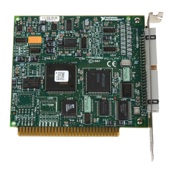
Introduction This chapter describes the PC-LPM-16/PnP, lists what you need to get started, software programming choices, and optional equipment, and explains how to unpack the PC-LPM-16/PnP. About the PC-LPM-16/PnP The PC-LPM-16/PnP is a low-cost, low-power analog input, digital, and timing I/O board for the PC. The board contains a 12-bit, successive-approximation, self-calibrating ADC with 16 analog inputs, 8 lines of TTL-compatible digital input, and 8 lines of digital output. -
Page 13: What You Need To Get Started
Chapter 1 Introduction What You Need to Get Started To set up and use your PC-LPM-16/PnP board, you will need the following: Software Programming Choices There are several options to choose from when programming your National Instruments DAQ and SCXI hardware. You can use LabVIEW, LabWindows/CVI, NI-DAQ, or register-level programming. -
Page 14: Ni-Daq Driver Software
An example of a low-level function is writing directly to registers on the DAQ device. NI-DAQ does not sacrifice the performance of National Instruments DAQ devices because it lets multiple devices operate at their peak performance. -
Page 15: Register-Level Programming
Sun SPARCstation) Figure 1-1. The Relationship between the Programming Environment, NI-DAQ, Register-Level Programming The final option for programming any National Instruments DAQ hardware is to write register-level software. Writing register-level programming software can be very time-consuming and inefficient and is not recommended for most users. -
Page 16: Optional Equipment
Optional Equipment National Instruments offers a variety of products to use with your PC-LPM-16/PnP board, including cables, connector blocks, and other accessories, as follows: • • • • For more specific information about these products, refer to your National Instruments catalogue or call the office nearest you. -
Page 17: Unpacking
• • Unpacking Your PC-LPM-16/PnP board is shipped in an antistatic package to prevent electrostatic damage to the board. Electrostatic discharge can damage several components on the board. To avoid such damage in handling the board, take the following precautions: •... -
Page 18: Installation And Configuration
6. Replace the cover. 7. Plug in and turn on your computer. The PC-LPM-16PnP is installed. National Instruments Corporation computer. be a tight fit, but do not force the board into place. back panel rail of the computer. Chapter PC-LPM-16/PnP User Manual... -
Page 19: Software Installation
Play boards. Application software can query the Configuration Manager to determine the resources assigned to each board without your involvement. The Plug and Play software is installed as a device driver or as an integral component of the computer BIOS. PC-LPM-16/PnP User Manual National Instruments Corporation... -
Page 20: Base I/O Address And Interrupt Selection
You can also lock the board resources when you use ICU. For additional information on ICU, contact Intel Corporation for a copy of Plug and Play Specification version 1.0a. Chapter 2 Installation and Configuration PC-LPM-16/PnP User Manual... -
Page 21: Theory Of Operation
The block diagram in Figure 3-1 shows a functional overview of the PC-LPM-16PnP. National Instruments Corporation PC I/O channel interface circuitry Analog input and data acquisition circuitry Digital I/O circuitry Timing I/O circuitry Chapter PC-LPM-16/PnP User Manual... -
Page 22: Figure 3-1. Pc-Lpm-16Pnp Block Diagram
Theory of Operation PC I/O Channel Interface Plug and Play 1 MHz Interrupt Interface +12 V -12 V +5 V PC-LPM-16/PnP User Manual 12-Bit 256-Word Sampling FIFO OUT0 A/D Timing CLK0 MSM82C53 FROM A/D FIFO Digital Figure 3-1. PC-LPM-16PnP Block Diagram... -
Page 23: Pc I/O Channel Interface Circuitry
Plug and Decoder Play Circuitry Timing Interface Data Buffers Plug and Play Interrupt Control Figure 3-2. PC I/O Interface Circuitry Block Diagram Chapter 3 Theory of Operation Register Selects Read & Write Signals Internal Data Bus Interrupt Requests PC-LPM-16/PnP User Manual... -
Page 24: Analog Input And Data Acquisition Circuitry
Interface CLK0 1 MHz PC-LPM-16/PnP User Manual When an A/D conversion generates data that can be read from FIFO When an active low-level signal is detected on the EXTINT* line When a rising-edge signal is detected on counter 2 output... -
Page 25: Analog Input Circuitry
16 bits by board circuitry so that data values read from the FIFO are 16 bits wide. The ADC on the PC-LPM-16PnP includes calibration circuitry that makes it possible to minimize zero, full-scale, and linearity errors. The National Instruments Corporation PC-LPM-16/PnP User Manual... -
Page 26: Data Acquisition Timing Circuitry
PC-LPM-16PnP can perform two types of data acquisition: single- channel data acquisition and multichannel scanning data acquisition. Multichannel scanning data acquisition uses a counter to automatically switch between analog input channels during a data acquisition operation. Data acquisition timing consists of signals that initiate a data acquisition operation and generate scanning clocks. -
Page 27: Single-Channel Data Acquisition
During multichannel scanning, the settling time of the input multiplexers and operational amplifier further limits the data acquisition rate. After the input multiplexers switch channels, the amplifier must be able to settle to the new input signal value to within 12-bit accuracy before performing an A/D conversion, or else it will not achieve 12-bit accuracy. -
Page 28: Digital I/O Circuitry
DIN<0..7> lines. Writing to the Digital Output Register drives the new value onto the DOUT<0..7> lines. The external device may drive the EXTINT* signal to indicate the readiness of data transfer. PC-LPM-16/PnP User Manual Digital Input I/O RD... -
Page 29: Timing I/O Circuitry
GA TE2 OUT2 Data MSM82C53 Counter/Timer Figure 3-5. Timing I/O Circuitry Block Diagram Chapter 3 Theory of Operation A/D Conversion Logic OUT0 GA TE0 CLK1 GA TE1 OUT1 OUT1* CLK2 GA TE2 OUT2 Plug and Play Interrupt Interface PC-LPM-16/PnP User Manual... -
Page 30: Figure 3-6. Counter Block Diagram
CLK, GATE, and OUT, respectively. The MSM82C53 counters are numbered zero through two, and their GATE, CLK, and OUT pins are labeled GATEN, CLKN, and OUTN, where N is the counter number. PC-LPM-16/PnP User Manual Counter GATE Figure 3-6. Counter Block Diagram... -
Page 31: Signal Connections
PC-LPM-16PnP can damage the board and the computer. This includes connecting any power signals to ground and vice versa. Each signal description in this section includes information about maximum input ratings. National Instruments is from any such signal connections. National Instruments Corporation... -
Page 32: Figure 4-1. Pc-Lpm-16Pnp I/O Connector Pin Assignments
Chapter 4 Signal Connections PC-LPM-16/PnP User Manual AIGND ACH0 ACH1 ACH2 ACH3 11 12 ACH4 13 14 ACH5 15 16 ACH6 17 18 ACH7 19 20 DGND 21 22 +12 V 23 24 DIN1 25 26 DIN3 27 28 DIN5... -
Page 33: Signal Connection Descriptions
DOUT7 is the MSB, DOUT0 the LSB. DGND Output of Counter 1—This signal outputs the inverted programmed waveform of counter 1. DGND External Interrupt—This pin is used for input of the external interrupt signal. Chapter 4 Signal Connections Description PC-LPM-16/PnP User Manual... -
Page 34: Table 4-1. Signal Connection Descriptions
GATE1 CLK1 OUT2 GATE2 CLK2 +5 V DGND Note: An asterisk (*) indicates that the signal is active low. PC-LPM-16/PnP User Manual Signal Connection Descriptions (Continued) Reference DGND External Convert Signal—This input signal externally initiates an A/D conversion. DGND Output of Counter 0—This signal outputs the programmed waveform of counter 0. -
Page 35: Analog Input Signal Connections
Warning: Exceeding the input signal range, even on unused analog input channels, distorts other input signals. Exceeding the maximum input voltage rating can damage your board and the computer. National Instruments is liable for any damages resulting from such signal connections. -
Page 36: Digital I/O Signal Connections
See Table 4-1 for the digital I/O pin descriptions. The following specifications and ratings apply to the digital I/O lines: • • • • • • PC-LPM-16/PnP User Manual ACH<0..15> Input Multiplexer 1, 2 AIGND PC-LPM-16PnP Figure 4-2. Analog Input Signal Connections Absolute maximum... -
Page 37: Power Connections
+5 V Debounced Switch* *Complex switch circuitry is not shown here in order to simplify the figure. Figure 4-3 shows the connections of the digital input port and digital output port. Digital input applications include receiving TTL signals and sensing external device states such as the switch in Figure 4-3. -
Page 38: Power Rating
EXTCONV*. The data from this conversion is latched into the FIFO memory within 20 s. The EXTCONV* input is a TTL-compatible signal. PC-LPM-16/PnP User Manual Power Line -12 V on your computer. Notice also that any current drawn from these lines adds to the power requirements from the computer. -
Page 39: General-Purpose Timing Signal Connections And General-Purpose Counter Timing Signals
You can gate the counter operation on and off during event counting. Figure 4-5 shows connections for a typical event-counting operation where a switch is used to gate the counter on and off. National Instruments Corporation w 200 ns min... -
Page 40: Figure 4-5. Event-Counting Application With External Switch Gating
Signal Source I/O Connector *Complex switch circuitry is not shown here in order to simplify the figure. Perform pulse-width measurement by level gating to trigger the counter. Apply the pulse to be measured to the counter GATE input. Load the counter with the known count and program it to count down while the signal at the GATE input is high. -
Page 41: Figure 4-6. Frequency Measurement Application
OUT output signals. The following specifications and ratings apply to the MSM82C53 I/O signals: • Absolute maximum voltage input rating -0.5 to 7.0 V with respect to DGND National Instruments Corporation 4-11 PC-LPM-16/PnP User Manual... -
Page 42: Figure 4-7. General-Purpose Timing Signals
• • GATE The GATE and OUT signals in Figure 4-7 are referenced to the rising edge of the CLK signal. PC-LPM-16/PnP User Manual input logic high voltage input logic low voltage Input load current output logic high voltage output logic low voltage... -
Page 43: Specifications
Offset error after calibration... 1.0 LSB typ, 2.0 LSB max National Instruments Corporation Inputs protected ... ACH<0..15> (For more information on nonlinearity and quantization error, see the Explanation of Analog Input Specifications section) Appendix 0 to 5 V, software-selectable 35 V powered off PC-LPM-16/PnP User Manual... -
Page 44: Dynamic Characteristics
Compatibility ...TTL Configuration...1 8-bit input port, Absolute max ratings ...+7.0 V with respect to DGND; PC-LPM-16/PnP User Manual 0 to 5 V and 5 V range ... 1.0 LSB typ, 2.0 LSB max All other ranges... 2.0 of reading typ, Gain = (-3 dB) ...200 kHz typ... - Page 45 (V in = 5 V) Level Output low voltage (I out = 4 mA) Output high voltage (I out = 4 mA) analog input) high with 4.7 k PC-LPM-16/PnP User Manual Specifications Minimum Maximum 0.8 V 5.0 V — 10 A —...
-
Page 46: Bus Interface
Thus, it is more specific to use relative accuracy as a measure of linearity than it is to use what is normally called nonlinearity, because relative accuracy ensures that the PC-LPM-16/PnP User Manual connector National Instruments Corporation... - Page 47 1 LSB of the ideal, one of its edges may be well beyond 1 LSB; thus, the ADC would have a relative accuracy of that amount. National Instruments tests its boards to ensure that they meet all three linearity specifications defined in this appendix;...
-
Page 48: Figure A-1. Adc Errors
LSBs. Finally, the differential nonlinearity is deviation of a code width from ideal code width, expressed in terms of LSBs. PC-LPM-16/PnP User Manual actual ideal = Center of code1 for ideal ADC... - Page 49 CMOS programmable interval timer (OKI Semiconductor). This timer is used on the PC-LPM-16PnP board. *Copyright All rights reserved. OKI Semiconductor Data Book Microprocessor, Eight Edition, January 1995. © National Instruments Corporation Semiconductor 1995. Reprinted with permission of copyright owner. Appendix PC-LPM-16/PnP User Manual...
- Page 50 Appendix B MSM82C53 Data Sheet PC-LPM-16/PnP User Manual © National Instruments Corporation...
- Page 51 Appendix B MSM82C53 Data Sheet © National Instruments Corporation PC-LPM-16/PnP User Manual...
- Page 52 Appendix B MSM82C53 Data Sheet PC-LPM-16/PnP User Manual © National Instruments Corporation...
- Page 53 Appendix B MSM82C53 Data Sheet © National Instruments Corporation PC-LPM-16/PnP User Manual...
- Page 54 Appendix B MSM82C53 Data Sheet PC-LPM-16/PnP User Manual © National Instruments Corporation...
- Page 55 Appendix B MSM82C53 Data Sheet © National Instruments Corporation PC-LPM-16/PnP User Manual...
- Page 56 Appendix B MSM82C53 Data Sheet PC-LPM-16/PnP User Manual © National Instruments Corporation...
- Page 57 Appendix B MSM82C53 Data Sheet © National Instruments Corporation PC-LPM-16/PnP User Manual...
- Page 58 Appendix B MSM82C53 Data Sheet PC-LPM-16/PnP User Manual B-10 © National Instruments Corporation...
- Page 59 Appendix B MSM82C53 Data Sheet © National Instruments Corporation B-11 PC-LPM-16/PnP User Manual...
- Page 60 Appendix B MSM82C53 Data Sheet PC-LPM-16/PnP User Manual B-12 © National Instruments Corporation...
-
Page 61: Table
PC-LPM-16 The PC-LPM-16PnP is a Plug and Play upgrade from a legacy board, the PC-LPM-16. A National Instruments legacy product refers to an older board with switches and jumpers used to set the addresses. The original board has been replaced with a backwards-compatible, revised PC-LPM-16. - Page 62 10 V Range 7 LSB max Calibration Time 700 s typ Overvoltage 45 V Protection or Analog Input Powered Off PC-LPM-16/PnP User Manual Comparison of Characteristics (Continued) Revised PC-LPM-16 512 words Not required, but allowed Low byte must be read before high...
-
Page 63: Table
(see Figure C-1). National Instruments Corporation Appendix C Comparison of Characteristics (Continued) Revised PC-LPM-16 Through Command Register 1 800 ns max Using Your PC-LPM-16 (Non-PnP) Board PC-LPM-16PnP Through Plug and Play BIOS or NI-DAQ Configuration Utility 800 ns max PC-LPM-16/PnP User Manual... - Page 64 The PC-LPM-16 contains three jumpers and one DIP switch to configure the PC bus interface and analog input settings. Use the DIP switch to set the base I/O address. Jumper W3 selects the interrupt level. Jumpers W1 and W2 configure the analog input circuitry. The DIP...
-
Page 65: Figure C-1. Pc-Lpm-16 Parts Locator Diagram
1 W3 3 W2 2 Switch U26 4 W1 National Instruments Corporation Appendix C Using Your PC-LPM-16 (Non-PnP) Board 5 Serial Number 6 Assembly Number Figure C-1. PC-LPM-16 Parts Locator Diagram 7 Product Name PC-LPM-16/PnP User Manual... -
Page 66: Pc Bus Interface Factory Settings
U26 (see Figure C-2). The switches are set at the factory for the base I/O address hex 260. This factory setting is used as the default base I/O address value by National Instruments software packages for use with the PC-LPM-16. The PC-LPM-16 uses the base I/O address space hex 260 through 26F with the factory setting. -
Page 67: Figure C-2. Example Base I/O Address Switch Settings
Each switch in U26 corresponds to one of the address lines A9 through A5. Slide the switch to the side labeled A9 to A5 to select a binary value of zero for the corresponding address bit. Slide the switch to the side of the switch labeled ON to select a binary value of one for the corresponding address bit. -
Page 68: Base I/O Address Space
Appendix C Using Your PC-LPM-16 (Non-PnP) Board possible switch settings, the corresponding base I/O address, and the base I/O address space used for that setting. A9 A8 A7 A6 A5 PC-LPM-16/PnP User Manual Table C-3. Switch Settings with Corresponding Base I/O Address and... -
Page 69: Interrupt Selection
Table C-3. Switch Settings with Corresponding Base I/O Address and Base I/O Address Space (Continued) Switch Setting Base I/O Address (hex) Using Your PC-LPM-16 (Non-PnP) Board Base I/O Address Space Used (hex) 340–34F 360–36F 380–38F 3A0–3AF 3C0–3CF 3E0–3EF PC-LPM-16/PnP User Manual... -
Page 70: Figure C-3. Interrupt Jumper Setting Irq5 (Factory Setting
Bipolar Input Selection 1 ( 5 V) Select the bipolar ( 5 V) input configuration by setting jumpers W1 and W2 as shown in Figure C-5. PC-LPM-16/PnP User Manual Figure C-3. Interrupt Jumper Setting IRQ5 (Factory Setting) Figure C-4. Interrupt Jumper Setting for Disabling Interrupts... -
Page 71: Figure C-5. Bipolar Input ( 5 V) Jumper Configuration (Factory Setting
Appendix C Figure C-5. Bipolar Input ( 5 V) Jumper Configuration (Factory Setting) Figure C-6. Bipolar Input ( 2.5 V) Jumper Configuration Figure C-7. Unipolar Input (0 to 10 V) Jumper Configuration C-11 Using Your PC-LPM-16 (Non-PnP) Board PC-LPM-16/PnP User Manual... - Page 72 PC-LPM-16, if possible. After you make any necessary changes with the jumper and switch settings, you are ready to install the PC-LPM-16.
-
Page 73: Pc-Lpm-16/Pnp Register Map
For information on the base address, see Chapter 2, Installation and Configuration. Register Map The register map for the PC-LPM-16/PnP is given in Table D-1. This table gives the register name, the register address offset from the board’s base address, the type of the register (read only, write only, or read and write), and the size of the register in bits. -
Page 74: Register Descriptions
The Configuration and Status Register Group controls the overall operation of the PC-LPM-16/PnP and the D/A circuitry. The Analog Input Register Group reads output from the successive-approximation ADC. The Counter/Timer Register Group accesses the onboard MSM82C53 counter/timer integrated circuit. -
Page 75: Register Description Format
Appendix D Register-Level Programming Register Description Format The remainder of this appendix discusses each of the PC-LPM-16/PnP registers in the order shown in Table D-1. Each register group is introduced, followed by an individual register description. The individual register description includes the address, type, word size, and bit map of the register. - Page 76 Bit Map: SCANEN* CNTINTEN EXTINTEN Name SCANEN* PC-LPM-16/PnP User Manual FIFOINTEN Description Scan Enable Bit—This bit enables or disables multichannel scanning during data acquisition. The power-on value is 1. If this bit is cleared, analog channels MA<3..0> through 0 are sampled alternately.
- Page 77 16 input channels are read. The power-on value is 0000. The analog input multiplexer depends on these four bits to select the input channel. The input channel is selected as follows: MA<3..0> 0000 0001 0010 0011 Register-Level Programming Selected Channel PC-LPM-16/PnP User Manual...
- Page 78 Appendix D Register-Level Programming Command Register 1 (Continued) PC-LPM-16/PnP User Manual MA<3..0> 0100 0101 0110 0111 1000 1001 1010 1011 1100 1101 1110 1111 If SCANEN* is cleared, analog channels MA<3..0> through channel 0 are sampled. Sampling order, whether from channel 0 to MA<3..0> or from MA<3..0>...
- Page 79 0. Upon startup, this bit is cleared and, as a result, the data acquisition operation is enabled. Writing a one to this bit disables both A/D conversion source signals OUT0* and EXTCONV*. Appendix D Register-Level Programming SCANORDER DISABDAQ CALEN PC-LPM-16/PnP User Manual...
- Page 80 Register-Level Programming Command Register 2 (Continued) Name CALEN PC-LPM-16/PnP User Manual Description Calibration Enable Bit—If this bit is set, the auto- calibration of the 12 bit ADC is enabled. The power- on value is 0. To start the auto-calibration, first write one to this bit, then read this register.
-
Page 81: Command Register 3
Analog Input Voltage Range—These bits control the analog input voltage range setting as follows: ARNG<1..0> The power-on value for ARNG<1..0> is 10. Appendix D Register-Level Programming ARNG<1> ARNG<0> Input Voltage Range 0 to 10 V 5 V, 0 to 5 V 2.5 V PC-LPM-16/PnP User Manual... -
Page 82: Status Register 1
Bit Map: REVID Name REVID 6–5 CONVPROG PC-LPM-16/PnP User Manual CONVPROG EXTINT* Description Revision ID Bit—This bit identifies the board revision. If this bit is cleared, the board is a revision A legacy PC-LPM-16 board. If this bit is set, the board is a revision B or later PC-LPM-16 board. - Page 83 OVERFLOW and OVERRUN bits in Status Register 2. Clear this bit by writing to the A/D Clear Register. On the PC-LPM-16PnP, this bit only indicates that an overflow has occurred. D-11 Register-Level Programming PC-LPM-16/PnP User Manual...
- Page 84 Appendix D Register-Level Programming DAVAIL PC-LPM-16/PnP User Manual Data Available Bit—This bit indicates whether conversion output is available. If this bit is set, the ADC is finished with the last conversion and the result can be read from the FIFO. This bit is cleared if the FIFO is empty.
-
Page 85: Status Register 2
(sample rate is too high). If OVERRUN is set, one or more conversions was skipped. If OVERRUN is cleared, no overrun condition has occurred. To clear this bit, write to the A/D Clear Register. D-13 Appendix D Register-Level Programming OVERFLOW OVERRUN PC-LPM-16/PnP User Manual... -
Page 86: Analog Input Register Group
Reading the FIFO Register returns stored A/D conversion results. Writing to the A/D Clear Register clears the data acquisition circuitry. Bit descriptions for the registers making up the Analog Input Register Group are given on the following pages. PC-LPM-16/PnP User Manual D-14 National Instruments Corporation... - Page 87 Bit Map: Two’s complement binary mode High Byte {---Sign and Sign Extension Bits---} Low Byte National Instruments Corporation MUST D-15 Appendix D Register-Level Programming be read first. Base address + 02 (hex) Base address + 03 (hex) PC-LPM-16/PnP User Manual...
- Page 88 Note: The ADC resolution is actually 13 bits, not 12 bits. NI-DAQ only returns a 12-bit value, and the PC-LPM-16/PnP boards are tested only to 12-bit accuracy. However, by writing register-level programming, you can use the full 13 bits. The ADC always returns values from -4,096 to +4,095. For unipolar mode, if you want 12-bit resolution instead of 13-bit, you should ignore any negative value, giving a range of 0 to +4.095.
- Page 89 A/D Clear Register, it is necessary to read both the High- and Low-Byte FIFOs. The data that is read back should be ignored. Address: Base address + 01 (hex) Type: Write-only Word Size: 8-bit Bit Map: Not applicable, no bits used National Instruments Corporation Appendix D Register-Level Programming D-17 PC-LPM-16/PnP User Manual...
- Page 90 2. Bit descriptions for the registers in the Counter/Timer Register Group are given in the following pages. PC-LPM-16/PnP User Manual D-18 National Instruments Corporation...
- Page 91 Use the Counter 0 Data Register to load and read back contents of MSM82C53 counter 0. Address: Base address + 08 (hex) Type: Read-and-write Word Size: 8-bit Bit Map: Name 7–0 D<7..0> National Instruments Corporation Description A/D Conversion Data Bits 7 through 0—8-bit counter 0 contents. D-19 Appendix D Register-Level Programming PC-LPM-16/PnP User Manual...
- Page 92 Base address + 0A (hex) Type: Read-and-write Word Size: 8-bit Bit Map: Name 7–0 D<7..0> PC-LPM-16/PnP User Manual Description A/D Conversion Data Bits 7 through 0—8-bit counter 1 contents. Description A/D Conversion Data Bits 7 through 0—8-bit counter 2 contents. D-20...
- Page 93 Bit Map: Name 7–6 SC<1..0> National Instruments Corporation Description Counter Select Bits—These bits select the counter on which the command operates. D-21 Appendix D Register-Level Programming Operation Select counter 1 Select counter 2 Select counter 3 Read-back command PC-LPM-16/PnP User Manual...
- Page 94 Register-Level Programming Counter Mode Register (Continued) 5–4 RL<1..0> PC-LPM-16/PnP User Manual Read/Write Select Bits—These bits select data written to or read from a counter, or these bits send a Counter Latch command. Counter Latch command Read and write least significant...
- Page 95 16-bit binary. D-23 Register-Level Programming Mode Mode 0—Interrupt on terminal count Mode 1—Hardware retriggerable one shot Mode 2—Rate generator Mode 3—Square wave mode Mode 4—Software retriggerable strobe Mode 5—Hardware retriggerable strobe PC-LPM-16/PnP User Manual...
-
Page 96: Digital Output Register
Base address + 04 (hex) Type: Write-only Word Size: 8-bit Bit Map: Name 7–0 D<7..0> PC-LPM-16/PnP User Manual Description 8-Bit Output Data 7 through 0—These eight bits control the digital output lines DOUT 0 through DOUT 7. D-24 National Instruments Corporation... -
Page 97: Digital Input Register
Word Size: 8-bit Bit Map: Name 7–0 D<7..0> National Instruments Corporation Appendix D Description 8-Bit Input Data Bit—These eight bits represent the logic state of the digital input lines DIN 0 through DIN 7. D-25 Register-Level Programming PC-LPM-16/PnP User Manual... -
Page 98: Register Programming Considerations
Register Programming Considerations The PC-LPM-16/PnP can only be used for 8-bit I/O transfers, so all the I/O read-and-write operations are 8-bit operations. Several write-only registers on the PC-LPM-16/PnP contain bits that control several independent pieces of the onboard circuitry. -
Page 99: Programming The Analog Input Circuitry
This sequence leaves the PC-LPM-16/PnP circuitry in the following state: • • • • • For additional details concerning the MSM82C53 counter/timer, see Appendix B, MSM82C53 Data Sheet. Programming the A/D Calibration The ADC is a self-calibration converter and a self-calibration cycle adjusts positive linearity and full-scale errors. - Page 100 FIFO overflow. Write to the A/D Clear Register to reset this error flag. PC-LPM-16/PnP User Manual A low to high transition on OUT0 or on EXTCONV* initiates A/D conversion. Clear the CALEN bit in Command Register 2 to enable counter 0 and the EXTCONV*.
-
Page 101: Unipolar Input Mode A/D Conversion Values
National Instruments Corporation Table D-2. Unipolar Input Mode A/D Conversion Values Input Voltage (Decimal) 9.9976 D-29 Appendix D Register-Level Programming A/D Conversion Result Range: 0 to +10 V (Hex) 0000 1,024 0400 2,048 0800 3,072 0C00 4,095 0FFF PC-LPM-16/PnP User Manual... -
Page 102: Bipolar Input Mode A/D Conversion Values
In a data acquisition operation, counter 0 continuously generates the conversion pulses. The software keeps track of the number of conversions that have occurred and turns off counter 0 PC-LPM-16/PnP User Manual Table D-3. Bipolar Input Mode A/D Conversion Values... - Page 103 In Step a., writing to the Counter Mode Register forces OUT0 to high. To finish programming counter 0, you must also write the most significant byte. However, this writing starts the counting, so perform this writing in step 4. D-31 Appendix D Register-Level Programming PC-LPM-16/PnP User Manual...
- Page 104 To stop the A/D conversion sequence, write 34 to the Counter 0 Mode Register. This stops the generation of pulses on OUT0. PC-LPM-16/PnP User Manual during the programming. Write 0 to the A/D Clear Register to empty the FIFO (8-bit write), then read the low and high bytes from the A/D FIFO (PC-LPM-16 only).
- Page 105 Write 0 to Command Register 2 to enable the A/D conversion. b. The next EXTCONV* signal initiates an A/D conversion. The operation must be serviced by reading the A/D FIFO Register every time an A/D conversion result becomes available. To D-33 Appendix D Register-Level Programming PC-LPM-16/PnP User Manual...
- Page 106 PC-LPM-16PnP for multiple A/D conversions on a single input channel. You can also program the PC-LPM-16/PnP for scanning analog input channels during the data acquisition operation. Analog channels N through 0 can be scanned, where N can be 1 through 15. Also, 0 through N can be scanned.
- Page 107 Command Register 1. You must set the SCANEN* bit during this first write to Command Register 1. The SCANEN* bit, however, must be cleared during the second write to Command Register 1. D-35 Appendix D Register-Level Programming PC-LPM-16/PnP User Manual...
- Page 108 Counter 0 has a fixed 1 MHz clock input and can be used as the sample interval counter of A/D conversion. Write and read operations to the MSM82C53 are 8-bit operations. For general programming details, refer to Appendix B, MSM82C53 Data Sheet. PC-LPM-16/PnP User Manual D-36 National Instruments Corporation...
-
Page 109: Electronic Services
Electronic Services Bulletin Board Support National Instruments has BBS and FTP sites dedicated for 24-hour support with a collection of files and documents to answer most common customer questions. From these sites, you can also download the latest instrument drivers, updates, and example programs. For recorded instructions on how to use the bulletin board and FTP services and for BBS automated information, call (512) 795-6990. -
Page 110: Telephone And Fax Support
Telephone and Fax Support National Instruments has branch offices all over the world. Use the list below to find the technical support number for your country. If there is no National Instruments office in your country, contact the source from which you purchased your software to obtain support. - Page 111 National Instruments for technical support helps our applications engineers answer your questions more efficiently. If you are using any National Instruments hardware or software products related to this problem, include the configuration forms from their user manuals. Include additional pages if necessary.
- Page 112 Complete a new copy of this form each time you revise your software or hardware configuration, and use this form as a reference for your current configuration. Completing this form accurately before contacting National Instruments for technical support helps our applications engineers answer your questions more efficiently.
- Page 113 Documentation Comment Form National Instruments encourages you to comment on the documentation supplied with our products. This information helps us provide quality products to meet your needs. Title: PC-LPM-16/PnP User Manual Edition Date: November 1996 Part Number: 320287C-01 Please comment on the completeness, clarity, and organization of the manual.
- Page 114 Symbols ˚ – +5 V National Instruments Corporation Value degrees negative of, or minus ohms percent plus or minus positive of, or plus square root of +5 VDC source signal Glossary PC-LPM-16/PnP User Manual...
- Page 115 Glossary AIGATE AIGND AISENSE ANSI AOGND ASIC BIOS CMOS PC-LPM-16/PnP User Manual amperes alternating current analog input channel signal analog-to-digital A/D converter analog input analog input gate signal analog input ground signal analog input sense signal American National Standards Institute...
- Page 116 EISA FIFO National Instruments Corporation counter data acquisition direct current direct memory access Extended Industry Standard Architecture Engineering Software Package farads first-in-first-out feet hour hexadecimal hertz input/output current, output high current, output low Glossary PC-LPM-16/PnP User Manual...
- Page 117 Glossary SCANCLK SCXI SISOURCE STARTSCAN PC-LPM-16/PnP User Manual Industry Standard Architecture light emitting diode least significant bit meter megabytes of memory most significant bit personal computer random access memory root mean square seconds samples scan clock signal Signal Conditioning eXtensions for Instrumentation...
- Page 118 National Instruments Corporation transistor-transistor logic volts volts direct current virtual instrument volts, input high volts, input low volts in volts, output high volts, output low Glossary PC-LPM-16/PnP User Manual...
- Page 119 A/D FIFO output binary modes, D-29 to D-30 clearing the circuitry, D-30 programming sequence, D-28 theory of operation, 3-5 to 3-6 © National Instruments Corporation analog input jumper settings, PC-LPM-16, C-10 to C-12 bipolar input selection 1 ( 5 V) C-10 to C-11 bipolar input selection 2 ( 2.5 V) C-11...
- Page 120 RL<1..0>, D-22 SC<1..0>, D-21 SCANEN*, D-4, D-33, D-34 to D-35 SCANORDER, D-7 block diagram of PC-LPM-16PnP, 3-2 PC-LPM-16/PnP User Manual board configuration. See configuration. bulletin board support, E-1 bus interface specifications, A-4 cables, custom, 1-5 to 1-6 CALEN bit, D-8, D-28...
- Page 121 Counter 1 Data Register, D-20 Counter 2 Data Register, D-20 Counter Mode Register, D-21 to D-23 overview, D-18 programming, D-36 © National Instruments Corporation register map, D-2 Timer Interrupt Clear Register, D-24 custom cables, 1-5 to 1-6 customer communication, xii, E-1 to E-2 D<7..0>...
- Page 122 GATE and CLK input signals, 4-11 to 4-12 timing specifications for OUT output signals, 4-11 to 4-12 hardware installation, 2-1 initializing PC-LPM-16/PnP, D-26 to D-27 input multiplexer, 3-5 installation. See also configuration. PC-LPM-16, C-12 PC-LPM-16PnP hardware, 2-1...
- Page 123 Counter 0, D-30 to D-32 using external timing, D-33 to D-34 with channel scanning, D-34 to D-35 multiplexer, input, 3-5 NI-DAQ driver software, 1-3 to 1-4 © National Instruments Corporation operation of PC-LPM-16PnP. See theory of operation. OUT signal counter block diagram, 3-10...
- Page 124 D-29 to D-30 clearing the circuitry, D-30 programming sequence, D-28 compared with application software, 1-4 digital I/O circuitry, D-35 initializing PC-LPM-16/PnP, D-26 to D-27 MSM82C53 counter/timer, D-36 multiple A/D conversions on single input channel using Counter 0, D-30 to D-32...
- Page 125 4-9 Status Register 1, D-10 to D-12 Status Register 2, D-13 switch settings. See configuration. system noise, A-5 © National Instruments Corporation technical support, E-1 to E-2 theory of operation analog input circuitry, 3-5 to 3-6 block diagram, 3-4...