Sign In
Upload
Manuals
Brands
JCM GLOBAL Manuals
Bank Note Validator
DBV-400
JCM GLOBAL DBV-400 Manuals
Manuals and User Guides for JCM GLOBAL DBV-400. We have
1
JCM GLOBAL DBV-400 manual available for free PDF download: Integration Manual
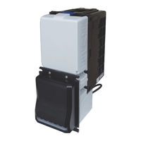
JCM GLOBAL DBV-400 Integration Manual (50 pages)
Brand:
JCM GLOBAL
| Category:
Bank Note Validator
| Size: 1.54 MB
Table of Contents
Table of Contents
3
1 General Information
9
Description
9
DBV-400 Unit
9
Figure 1 DBV-400 Unit
9
Model Descriptions
10
Type Descriptions
10
Software Descriptions
10
Precautions
10
User Cautions
10
Installation Cautions
10
Figure 2 Precautionary Symbols
10
Table 1 DBV-400 Model Number Specifications
10
Table 2 DBV-400 Type Number Specifications
10
Table 3 DBV-400 Software Number Specifications
10
Mounting, Dismounting & Transportation
11
Placing Foreign Objects into the Unit
11
Preventive Maintenance
11
Banknote Fitness Requirements
12
Primary Features
12
Figure 3 Unacceptable Banknotes
12
Component Names
13
Figure 4 DBV-400 Component Names
13
2 Specifications
14
Technical Specifications
14
Environmental Specifications
14
Table 4 DBV-400 Technical Specifications
14
Table 5 DBV-400 Environmental Specifications
14
Electrical Specifications
15
Structural Specifications
15
Table 6 DBV-400 Electrical Specifications
15
Table 7 DBV-400 Structural Specifications
15
3 Installation
16
Installation Procedure
16
Entire Unit Installation
16
DIP Switch Configurations
16
Figure 5 Thread Studs Location
16
Table 8 DIP Switch Block 1 Settings
16
Table 9 DIP Switch Block 2 Settings
16
4 Connector Pin Assignments
17
MDB Photo-Coupler Isolation Connector Pin Assignments
17
Table 10 DBV-400 CN1 ID-003 MDB Photo-Coupler Isolation Connector Pin Assignments
17
RS232 Connector Pin Assignments
18
Table 11 DBV-400 CN1 ID-003 RS232 Connector Pin Assignments
18
TTL Connector Pin Assignments
19
Table 12 DBV-400 CN1 ID-003 TTL Connector Pin Assignments
19
ID-002 Pulse Connector Pin Assignments
20
Table 13 DBV-400 CN1 ID-002 Pulse Connector Pin Assignments
20
ID-044 Pulse Connector Pin Assignments
21
Table 14 DBV-400 CN1 ID-044 Pulse Connector Pin Assignments
21
ID-044 Serial Connector Pin Assignments
22
Table 15 DBV-400 CN1 ID-044 Serial Connector Pin Assignments
22
USB Connector Pin Assignments
23
Table 16 DBV-400 CN2 USB Interface Connector Pin Assignments
23
Table 17 DBV-400 CN5 USB Maintenance Interface Connector Pin Assignments
23
5 Preventive Maintenance
24
Retrieving Banknotes
24
Clearing a Banknote Jam
24
Figure 6 Retrieving Banknotes 1
24
Figure 7 Retrieving Banknotes 2
24
Figure 8 Clearing a Banknote Jam 1
24
Figure 9 Clearing a Banknote Jam 2
24
Figure 10 Clearing a Banknote Jam 3
24
Cleaning Procedure
25
Sensor and Roller Cleaning Procedure
25
Figure 11 General Cleaning Image
25
Sensor and Roller Locations
26
Figure 12 DBV-400 Sensor and Roller Cleaning Locations
26
Table 18 DBV-400 Sensor Type Cleaning Methods
26
6 Standard Interface Circuit Schematics
27
Figure 13 DBV-400 ID-003 MDB Photo-Coupler Isolation Interface Schematic Diagram
27
Standard Interface Circuit Schematics (Continued 1)
28
Figure 14 DBV-400 ID-003 RS232C Interface Schematic Diagram
28
Standard Interface Circuit Schematics (Continued 2)
29
Figure 15 DBV-400 ID-003 TTL Interface Schematic Diagram
29
Standard Interface Circuit Schematics (Continued 3)
30
Figure 16 DBV-400 ID-002 Pulse Interface Schematic Diagram
30
Standard Interface Circuit Schematics (Continued 4)
31
Figure 17 DBV-400 ID-044 Pulse Interface Schematic Diagram
31
Standard Interface Circuit Schematics (Continued 5)
32
Figure 18 DBV-400 ID-044 Serial Interface Schematic Diagram
32
Standard Interface Circuit Schematics (Continued 6)
33
Figure 19 DBV-400 USB Interface Schematic Diagram
33
7 Operational Flowchart
35
Figure 20 DBV-400 Operational Flowchart (Initializing)
35
Operational Flowchart (Continued 1)
36
Figure 21 DBV-400 Operational Flowchart (Validation)
36
Figure 22 DBV-400 Operational Flowchart (Stacking)
36
8 Troubleshooting
37
Introduction
37
Troubleshooting Overview
37
Fault Table Listings
37
Table 19 General Fault Conditions
37
Adjustment Error
38
Communication Error
38
Table 20 Adjustment Fault Conditions
38
Table 21 Communication Fault Conditions
38
LED Indication Conditions
39
LED Flash Error Code Conditions
39
Table 22 LED Flash Error Codes
39
LED Flash Reject Code Conditions
41
Table 23 LED Flash Reject Codes
41
9 Unit Dimensions
43
Entire Unit Outside Dimensions
43
Figure 23 DBV-400 Unit with JCM Standard Bezel Outside Dimensions
43
Figure 24 DBV-400 Unit with Snack Mask Bezel Outside Dimensions
43
Entire Unit Outside Dimensions (Continued)
44
Figure 25 DBV-400 Unit with TOB Type Bezel Outside Dimensions
44
10 Technical Contact Information
45
Americas
45
JCM American
45
Europe, Africa, Russia & Middle East
45
JCM Europe Gmbh
45
UK & Ireland
45
JCM Europe (UK Office)
45
Asia and Oceania
45
JCM Gold (HK) Ltd
45
Japan Cash Machine Co., Ltd. (Hq)
45
11 Index
47
Advertisement
Advertisement
Related Products
JCM GLOBAL DBV Series
JCM GLOBAL DBV-500
JCM GLOBAL DT-300 Series
JCM GLOBAL iVIZION2 Series
JCM GLOBAL RDM-100 Series
JCM GLOBAL Taiko PUB-11
JCM GLOBAL Taiko PUB-7
JCM GLOBAL TBV Series
JCM GLOBAL TBV-100 FLD
JCM GLOBAL TBV-100 FSH
JCM GLOBAL Categories
Bank Note Validator
Industrial Equipment
Cash Register
Ultrasonic Jewelry Cleaner
Payment Terminal
More JCM GLOBAL Manuals
Login
Sign In
OR
Sign in with Facebook
Sign in with Google
Upload manual
Upload from disk
Upload from URL