Sign In
Upload
Manuals
Brands
Advantech Manuals
DC Drives
Automation1 XC4e
Advantech Automation1 XC4e Manuals
Manuals and User Guides for Advantech Automation1 XC4e. We have
1
Advantech Automation1 XC4e manual available for free PDF download: Hardware Manual
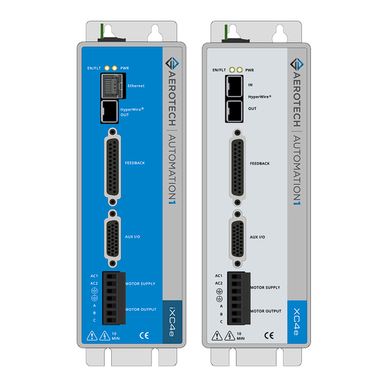
Advantech Automation1 XC4e Hardware Manual (124 pages)
PWM High-Performance Digital Drives
Brand:
Advantech
| Category:
DC Drives
| Size: 17.75 MB
Table of Contents
Automation1 Ixc4E and Xc4E PWM High-Performance Digital Drives
1
Table of Contents
3
List of Figures
5
List of Tables
7
EU Declaration of Conformity
9
Agency Approvals
11
Safety Procedures and Warnings
13
Installation Overview
15
Chapter 1: Introduction
17
Figure 1-1: Ixc4E Digital Drive-Based Controller
17
Figure 1-2: Xc4E Digital Drive
18
Table 1-1: Features and Options
19
Figure 1-3: Functional Diagram
20
Electrical Specifications
21
Table 1-2: Electrical Specifications
21
System Power Requirements
22
Mechanical Specifications
23
Mounting and Cooling
23
Table 1-3: Mounting Specifications
23
Dimensions
24
Figure 1-4: Dimensions
24
Figure 1-5: Dimensions [-EB1]
25
Environmental Specifications
26
Table 1-4: Environmental Specifications
26
Drive and Software Compatibility
27
Table 1-5: Drive and Software Compatibility
27
Chapter 2: Installation and Configuration
29
Input Power Connections
30
Control Supply Connector
30
Figure 2-1: Control Supply Connections
30
Table 2-1: Control Supply Wiring Specifications
30
Table 2-2: Mating Connector Part Numbers for the Control Supply Connector
30
Motor Supply Connector
31
Figure 2-2: Motor Supply Connections
31
Table 2-3: Motor Supply Connector Wiring Specifications
31
Table 2-4: Mating Connector Part Numbers for the Motor Supply Connector
31
Transformer Options
32
Table 2-5: Nominal Motor Operating Voltages / Required AC Voltages
32
Table 2-6: Transformer Options
32
Figure 2-3: TV0.3-28-56-ST Transformer Control and Motor Power Wiring (40 VDC Bus)
33
Figure 2-4: TV0.3-28-56-ST Transformer Control and Motor Power Wiring (80 VDC Bus)
34
Figure 2-5: TV0.3-28-56-ST Transformer Control and Motor Power Wiring (160 VDC Bus)
35
Figure 2-6: TV0.3-28 Transformer Control and Motor Power Wiring (40 VDC Bus)
36
Figure 2-7: TV0.3-56 Transformer Control and Motor Power Wiring (80 VDC Bus)
37
Figure 2-8: TM3/TM5 Transformer Control and Motor Power Wiring
38
Minimizing Noise for EMC/CE Compliance
39
Motor Power Output Connector
40
Table 2-7: Motor Power Output Connector Pinout
40
Table 2-8: Mating Connector Part Numbers for the Motor Power Output Connector
40
Brushless Motor Connections
41
Figure 2-9: Brushless Motor Configuration
41
Table 2-9: Wire Colors for Aerotech-Supplied Brushless Motor Cables
41
Brushless Motor Powered Motor and Feedback Phasing
42
Figure 2-10: Positive Motor Direction
42
Figure 2-11: Encoder and Hall Signal Diagnostics
42
Table 2-10: Hall Signal Diagnostics
42
Brushless Motor Unpowered Motor and Feedback Phasing
43
Figure 2-12: Brushless Motor Phasing Oscilloscope Example
43
Figure 2-13: Brushless Motor Phasing Goal
43
DC Brush Motor Connections
44
Figure 2-14: DC Brush Motor Configuration
44
Table 2-11: Wire Colors for Aerotech-Supplied DC Brush Motor Cables
44
DC Brush Motor Phasing
45
Figure 2-15: Positive Motor Direction
45
Stepper Motor Connections
46
Figure 2-16: Stepper Motor Configuration
46
Table 2-12: Wire Colors for Aerotech-Supplied Stepper Motor Cables
46
Stepper Motor Phasing
47
Figure 2-17: Positive Motor Direction
47
Feedback Connector
48
Table 2-13: Feedback Connector Pinout
48
Table 2-14: Mating Connector Part Numbers for the Feedback Connector
48
Primary Encoder Inputs
49
Table 2-15: Multiplier Options
49
Table 2-16: Primary Encoder Input Pins on the Feedback Connector
49
Square Wave Encoder
50
Figure 2-18: Square Wave Encoder Schematic (Feedback Connector)
50
Table 2-17: Square Wave Encoder Specifications
50
Absolute Encoder
51
Figure 2-19: Absolute Encoder Schematic (Feedback Connector)
51
Sine Wave Encoder [-MX2/-MX3 Option]
52
Figure 2-20: Sine Wave Encoder Phasing Reference Diagram
52
Table 2-18: Sine Wave Encoder Specifications
52
Figure 2-21: Sine Wave Encoder Schematic (Feedback Connector)
53
Encoder Phasing
54
Figure 2-22: Encoder Phasing Reference Diagram (Standard)
54
Figure 2-23: Position Feedback in the Diagnostic Display
54
Hall-Effect Inputs
55
Figure 2-24: Hall-Effect Inputs Schematic (Feedback Connector)
55
Table 2-19: Hall-Effect Feedback Pins on the Feedback Connector
55
Thermistor Input
56
Figure 2-25: Thermistor Input Schematic (Feedback Connector)
56
Table 2-20: Thermistor Input Pin on the Feedback Connector
56
Encoder Fault Input
57
Figure 2-26: Encoder Fault Input Schematic (Feedback Connector)
57
Table 2-21: Encoder Fault Input Pin on the Feedback Connector
57
End of Travel and Home Limit Inputs
58
Table 2-22: End of Travel and Home Limit Pins on the Feedback Connector
58
Figure 2-27: End of Travel and Home Limit Input Connections
59
Figure 2-28: End of Travel and Home Limit Input Schematic (Feedback Connector)
59
End of Travel and Home Limit Phasing
60
Figure 2-29: End of Travel and Home Limit Input Diagnostic Display
60
Brake Outputs
61
Figure 2-30: Brake Connected to the 25-Pin Feedback Connector (Typical)
61
Table 2-23: Brake Output Pins on the Feedback Connector
61
Table 2-24: Brake Control Specifications
61
Safe Torque off Input (STO)
62
Table 2-25: STO Connector Pinout
62
Table 2-26: Mating Connector Part Numbers for the STO Connector
62
Figure 2-31: Typical Configuration
63
Table 2-27: STO Electrical Specifications
63
STO Standards
64
Table 2-28: STO Standards
64
Table 2-29: STO Standards Data
64
STO Functional Description
65
STO Startup Validation Testing
66
Table 2-30: STO Signal Delay
66
Table 2-31: Motor Function Relative to STO Input State
66
STO Diagnostics
67
Figure 2-32: STO Timing
67
Table 2-32: STO Timing
67
Auxiliary I/O Connector
68
Table 2-33: Auxiliary I/O Connector Pinout
68
Table 2-34: Mating Connector Part Numbers for the Auxiliary I/O Connector
68
Auxiliary Encoder Inputs
69
Table 2-35: Auxiliary Encoder Pins on the Auxiliary I/O Connector
69
Square Wave Encoder
70
Figure 2-33: Square Wave Encoder Interface (aux I/O Connector)
70
Table 2-36: Square Wave Encoder Specifications
70
Absolute Encoder
71
Figure 2-34: Absolute Encoder Schematic (Auxiliary I/O Connector)
71
Sine Wave Encoder [-MX3 Option]
72
Figure 2-35: Sine Wave Encoder Phasing Reference Diagram
72
Table 2-37: Sine Wave Encoder Specifications
72
Figure 2-36: Sine Wave Encoder Schematic (Auxiliary I/O Connector)
73
Position Synchronized Output (PSO)
74
Table 2-38: PSO Specifications
74
Table 2-39: PSO Pins on the Auxiliary I/O Connector
74
Figure 2-37: PSO Interface
75
Digital Outputs
76
Table 2-40: Digital Output Specifications
76
Table 2-41: Digital Output Pins on the Auxiliary I/O Connector
76
Figure 2-38: Digital Output Schematic (aux I/O Connector)
77
Figure 2-39: Digital Outputs Connected in Current Sourcing Mode
78
Figure 2-40: Digital Outputs Connected in Current Sinking Mode
78
Digital Inputs
79
Figure 2-41: Digital Inputs Schematic (aux I/O Connector)
79
Table 2-42: Digital Input Specifications
79
Table 2-43: Digital Input Pins on the Auxiliary I/O Connector
79
Figure 2-42: Digital Inputs Connected to Current Sourcing Devices
80
Figure 2-43: Digital Inputs Connected to Current Sinking Devices
80
High-Speed Inputs
81
Figure 2-44: High-Speed Inputs
81
Table 2-44: High-Speed Input Specifications
81
Table 2-45: High-Speed Input Pins on the Auxiliary I/O Connector
81
Analog Output
82
Figure 2-45: Analog Output 0 Schematic
82
Table 2-46: Analog Output Specifications
82
Table 2-47: Analog Output Pins on the Auxiliary I/O Connector
82
Analog Input 0 (Differential)
83
Figure 2-46: Analog Input 0 Schematic
83
Table 2-48: Analog Input Specifications
83
Table 2-49: Analog Input Pins on the Auxiliary I/O Connector
83
Brake Power Supply Connector
84
Table 2-50: Brake Power Supply Connector Pinout
84
Table 2-51: Mating Connector Part Numbers for the Brake Power Supply Connector
84
Hyperwire Interface
85
Table 2-52: Hyperwire Card Part Number
85
Table 2-53: Hyperwire Cable Part Numbers
85
External Shunt Option [-SX1]
86
Table 2-54: -SX1 Component Information
86
Table 2-55: Maximum Additional Storage Energy for a Standard Ixc4E/Xc4E
87
Sync Port
88
Table 2-56: Sync-Related Functions
88
Table 2-57: Sync Port Cables
88
System Interconnection
89
Figure 2-47: Drive-Based System Wiring Drawing (Best Practice)
89
Figure 2-48: PC-Based System Wiring Drawing (Best Practice)
89
Figure 2-49: Drive-Based Controller System Interconnection (Best Practice)
90
Figure 2-50: PC-Based Controller System Interconnection (Best Practice)
91
PC Configuration and Operation Information
92
Chapter 3: -EB1 I/O Option Board
93
Figure 3-1: -EB1 I/O Option Board Connectors (Ixc4E Shown)
93
Digital Outputs [-EB1]
94
Table 3-1: Digital Output Specifications [-EB1]
94
Table 3-2: Digital Output 1 Connector Pinout [-EB1]
95
Table 3-3: Mating Connector Part Numbers for the Digital Output 1 Connector [-EB1]
95
Table 3-4: Digital Output 2 Connector Pinout [-EB1]
95
Table 3-5: Mating Connector Part Numbers for the Digital Output 2 Connector [-EB1]
95
Figure 3-2: Digital Outputs Schematic [-EB1]
96
Figure 3-3: Digital Outputs Connected in Current Sourcing Mode [-EB1]
97
Figure 3-4: Digital Outputs Connected in Current Sinking Mode [-EB1]
97
Digital Inputs [-EB1]
98
Table 3-6: Digital Input Specifications [-EB1]
98
Table 3-7: Digital Input 1 Connector Pinout [-EB1]
98
Table 3-8: Mating Connector Part Numbers for the Digital Input 1 Connector [-EB1]
98
Figure 3-5: Digital Inputs Schematic [-EB1]
99
Table 3-9: Digital Input 2 Connector Pinout [-EB1]
99
Table 3-10: Mating Connector Part Numbers for the Digital Input 2 Connector [-EB1]
99
Figure 3-6: Digital Inputs Connected to Current Sourcing (PNP) Devices [-EB1]
100
Figure 3-7: Digital Inputs Connected to Current Sinking (NPN) Devices [-EB1]
100
Analog Outputs [-EB1]
101
Figure 3-8: Analog Output Typical Connection [-EB1]
101
Table 3-11: Analog Output Specifications [-EB1]
101
Table 3-12: Analog Output Connector Pinout [-EB1]
101
Table 3-13: Mating Connector Part Numbers for the Analog Output Connector [-EB1]
101
Analog Inputs [-EB1]
102
Figure 3-9: Analog Input Typical Connection [-EB1]
102
Table 3-14: Differential Analog Input Specifications [-EB1]
102
Table 3-15: Analog Input Connector Pinout [-EB1]
102
Table 3-16: Mating Connector Part Numbers for the Analog Input Connector [-EB1]
102
Position Synchronized Output Interface [-EB1]
103
Table 3-17: PSO Specifications [-EB1]
103
Table 3-18: PSO Interface Connector Pinout [-EB1]
103
Table 3-19: Mating Connector Part Numbers for the PSO Interface Connector [-EB1]
103
Figure 3-10: PSO Output Sources Current
104
Figure 3-11: PSO Output Sinks Current
104
Figure 3-12: PSO TTL Outputs Schematic
104
Chapter 4: Cables and Accessories
105
Table 4-1: Standard Interconnection Cables
105
Joystick Interface
106
Figure 4-1: Two Axis Joystick Interface (to the aux I/O of Two Drives)
106
Figure 4-2: Two Axis Joystick Interface (to the I/O Board)
107
Handwheel Interface
108
Figure 4-3: Handwheel Interconnection to aux I/O Connector
108
Figure 4-4: Handwheel Interconnection to the aux I/O through a BBA32 Module
108
Chapter 5: Maintenance
109
Table 5-1: LED Description
109
Table 5-2: Troubleshooting
109
Preventative Maintenance
110
Table 5-3: Preventative Maintenance
110
Fuse Specifications
111
Table 5-4: Control Board Fuse Specifications
111
Appendix A: Warranty and Field Service
113
Appendix B: Revision History
115
Index
117
Advertisement
Advertisement
Related Products
Advantech Automation1 XC4
Advantech Automation1 iXC4
Advantech Automation1 iXC4e
Advantech ADAM-4571S
Advantech ADAM-5056SO
Advantech ADAM-5050
Advantech AMT-73
Advantech ADAM-5081
Advantech ADAM-4050
Advantech AMAX-5051T
Advantech Categories
Motherboard
Computer Hardware
Desktop
Touch Panel
PCI Card
More Advantech Manuals
Login
Sign In
OR
Sign in with Facebook
Sign in with Google
Upload manual
Upload from disk
Upload from URL