Denon S-302 Service Manual
Dvd home entertainment system
Hide thumbs
Also See for S-302:
- Owner's manual (63 pages) ,
- Quick setup manual (5 pages) ,
- Code list (3 pages)
Advertisement
Quick Links
QQ
3 7 63 1515 0
S-302
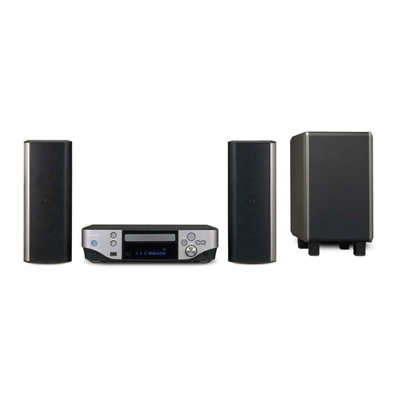
HOME THEATER SYSTEM (S-302) consists of DVD SURROUND RECEIVER (ADV-S302),
SUB WOOFER (DSW-S302) and SPEAKER SYSTEM (SC-S302)
TE
L 13942296513
For purposes of improvement, specifications and
design are subject to change without notice.
Please use this service manual with referring to the
operating instructions without fail.
Some illustrations using in this service manual are
slightly different from the actual set.
www
.
http://www.xiaoyu163.com
SERVICE MANUAL
MODEL
DVD HOME ENTERTAINMENT SYSTEM
x
ao
y
i
Denon Brand Company, D&M Holdings lnc.
http://www.xiaoyu163.com
8
JP
E3
E2
Q Q
3
6 7
1 3
u163
TOKYO, JAPAN
.
2 9
9 4
2 8
Ver. 3
Please refer to the
MODIFICATION NOTICE.
EK
E2A E1C E1K EUT
1 5
0 5
8
2 9
9 4
m
co
X0335 V.03 DE/CDM 0801
9 9
2 8
9 9
Advertisement

Related Manuals for Denon S-302


Summary of Contents for Denon S-302
- Page 1 MODEL E2A E1C E1K EUT S-302 DVD HOME ENTERTAINMENT SYSTEM HOME THEATER SYSTEM (S-302) consists of DVD SURROUND RECEIVER (ADV-S302), SUB WOOFER (DSW-S302) and SPEAKER SYSTEM (SC-S302) L 13942296513 For purposes of improvement, specifications and design are subject to change without notice.
- Page 2 S-302 3 7 6 3 1 5 1 5 0 SAFETY PRECAUTIONS The following check should be performed for the continued protection of the customer and service technician. LEAKAGE CURRENT CHECK Before returning the unit to the customer, make sure you make either (1) a leakage current check or (2) a line to chassis resistance check.
- Page 3 S-302 DIMENSION 3 7 63 1515 0 ADV-S302 L 13942296513 u163 http://www.xiaoyu163.com...
- Page 4 S-302 DSW-S302 3 7 63 1515 0 L 13942296513 u163 http://www.xiaoyu163.com...
- Page 5 S-302 SC-S302 3 7 63 1515 0 L 13942296513 u163 http://www.xiaoyu163.com...
- Page 6 S-302 WIRE ARRANGEMENT 3 7 63 1515 0 If wire bundles are untied or moved to perform adjustment or parts replacement etc., be sure to rearrange them neatly as they were originally bundled or placed afterward. Otherwise, incorrect arrangement can be a cause of noise generation.
- Page 7 S-302 3 7 63 1515 0 Fasten the CX061 6P connector cord with a cord holder. CX061 Ferrite Cramp L 13942296513 u163 http://www.xiaoyu163.com...
- Page 8 S-302 2. DSW-302 3 7 63 1515 0 2. DSW-302 Fasten the CX041 4P connector cord to the chassis with a clamp band. Fasten the CW041 4P connector cord and CX081 8P con- nector cord to the chassis with a clamp band.
- Page 9 S-302 DISASSEMBLY 3 7 63 1515 0 (Follow the procedure below in reverse order when reassem- bling.) ADV-S302 1. Side panel (1) Remove 4 screws 104 on the rear side and 4 screws 104 on the bottom side. (2) Detach the Side panel.
- Page 10 S-302 3. Drive unit 3 7 63 1515 0 3.1. When the Disc tray can be ejected electrically. (1) Switch on, and press [ (OPEN/CLOSE)] button to open the Disc tray. (2) Detach the Loader panel by lifting. (3) Close the Disc tray.
- Page 11 S-302 4. Front panel assy 3 7 63 1515 0 (1) Remove 3 screws 106 on the bottom side. (2) Disconnect the Wire [CX051],[CX052] and the FFC cable [CX211] from the Main unit and the Wire [CX054] from the USB unit.
- Page 12 S-302 5. Rear panel assy 3 7 63 1515 0 (1) Remove 10 screws 103 on the top side. (2) Remove 5 screws 105 on the rear side and 4 screws 105 on the both sides. (3) Detach the Rear panel assy.
- Page 13 S-302 DSW-S302 3 7 63 1515 0 1. Rear panel (1) Remove 10 screws 101 on the bottom side. (2) Detach the Rear panel. L 13942296513 2. SHIELD COVER (1) Remove 8 screws 103 on the Side. (2) Lift the shield cover using a flat-headed screwdriver and remove it.
- Page 14 S-302 ATTACHING THE ANTI-SLIP PADS 3 7 63 1515 0 Attach the anti-slip pads as shown on the diagram below. Press firmly so they do not peel off subsequently. Speaker stand Wall bracket L 13942296513 u163 http://www.xiaoyu163.com...
- Page 15 S-302 DIAGNOSTICS OF OPTICAL PICKUP 3 7 63 1515 0 AND REPLACING TRAVERSE UNIT Make failure diagnostics of the Optical Pickup as follows. If the laser drive current (Iop) becomes more than 1.5 times of the initial value, the Optical Pickup should be replaced.
- Page 16 S-302 1. Iop checked Method 3 7 63 1515 0 Select the laser ON/OFF (CD/DVD) mode of the test mode, and check the lop value of DVD laser or CD laser. (See page 21 for test mode.) 1.1. DVD laser current check...
- Page 17 S-302 4. Rewriting the default value of the laser 3 7 63 1515 0 current To rewrite the default value of the laser current, press the button for at least 5 seconds while the CD or DVD laser current is displayed, then press the button to select T23.
- Page 18 S-302 HOW TO REPLACE TRAVERSE UNIT 3 7 6 3 1 5 1 5 0 3. Traverse Unit disassembly (1) Remove 24P FFC, 15P FFC and 5P PH WIRE connect- Caution: The optical pickup can be damaged easily by ing with from the Main P.W.B.
- Page 19 S-302 SERVICE MODE 3 7 6 3 1 5 1 5 0 1. Aging Mode 1.1. preparation0 (1) Equipment used: Any one of DVD Karaoke Disc (containing more than 10 titles). (ex : Heat run disc TDV-HR01) (2) Unit setting : No spec other than the following procedure.
- Page 20 S-302 2. Initial Setting Mode 3 7 6 3 1 5 1 5 0 2.1. Preparation (1) Equipment used: None (2) Unit setting: No spec other than the following procedure. 2.2. Procedure SYSTEM This initializes the data for the function, volume, DVD mechanism, etc.
- Page 21 S-302 4. Test mode 3 7 6 3 1 5 1 5 0 4.1. Entering the test mode To enter the test mode, press the buttons simultaneously while in the Aging mode. Not insert the disc. (The Aging mode is entered by pressing the buttons simultaneously to turn on the AC power.
- Page 22 S-302 4.3. Setting the mode 3 7 6 3 1 5 1 5 0 With the mode selected, press the button to set that mode. In the laser on/off (CD/DVD) mode, laser on/off control is executed and the laser current is displayed.
- Page 23 S-302 4.4. Change within the mode 3 7 6 3 1 5 1 5 0 Changes within modes are made by pressing the buttons while the mode is set. In the laser on/off (CD/DVD) mode, laser on/off control is executed and the laser current is displayed.
- Page 24 S-302 4.5. Execution of trace mode (error rate display) (See "Table 2 - Trace mode details") 3 7 6 3 1 5 1 5 0 Trace will be performed if the button is pushed after choosing operation. (YY : selection mode [71 to 94], m : address [PBA][HEX], l : error rate [COUNT/SEC] [HEX]) Note) CD : Error rate of 75 frames is displayed (1 second).
- Page 25 S-302 3 7 6 3 1 5 1 5 0 Table 2: Trace mode details Contents Contents supplement A display of PO error detection number of the inner circumference It is invalid at the time of CD operation. of 1-layer and an address.
- Page 26 S-302 3 7 6 3 1 5 1 5 0 TROUBLE SHOOTING ADV-S302 1. 1U-3808 (MAIN UNIT) 1.1. FL TUBE dosen't light (1) Check the Set-up process of System -COM Check Power Supply Voltages. 1U-3808-1(MAIN UNIT) [IC303]: Check Soldering.
- Page 27 S-302 3 7 6 3 1 5 1 5 0 (2) Check the Set-up process of SUB -COM Check Power Supply Voltages. 1U-3808-1(MAIN UNIT) [IC301]: Check Soldering. +3.3V_D1 IC305 on MAIN UNIT. O.K. Check Reset signal. 1U-3808-1(MAIN UNIT) [IC301]:[SUB_RST]17 pin.
- Page 28 S-302 3 7 6 3 1 5 1 5 0 (3) Check the Set-up process of B/E -COM Check Power Supply Voltages. 1U-3808-1(MAIN UNIT) Check Soldering. [IC101]: [IC305] +3.3V_D2,+2.0V_ESS O.K.? [IC111] O.K. Check Clock waveform. Check 27MHz(3.3V)at (1) Check Soldering. of X101.
- Page 29 S-302 3 7 6 3 1 5 1 5 0 1.2. No Sound,Noise generated [No Play], [00 00] displayed etc. (1) CD,DVD PLAY (1) Check Soldering of P.U. short-circuit? Check the Emission of Pick-up. (2) Check the circumference soldering of TR603 IU-3807(FEP UNIT) and TR604.
- Page 30 S-302 3 7 6 3 1 5 1 5 0 1.3. No Sound,Noise generated (1) CD,DVD PLAY Check Power Supply Voltages. 1U-3808(MAIN UNIT) Check Soldering. +12V_A1,-12V_A1 CX801 +7V,-7V of [IC601] IC602,IC603 +1.2V_DSP of [IC401] IC404 O.K. Check Reset signal of [IC401], [IC501],[IC502].
- Page 31 S-302 3 7 6 3 1 5 1 5 0 Check Analog Audio Data output from CODEC to AMP. Check Soldering. 1U-3808(MAIN UNIT) [IC501]:28,29,31pin [IC501]output and [IC506],[IC507] [IC506],[IC507] [FL],[FR],[SW] O.K. Check audio mute signal. Check Soldering. 1U-3808(MAIN UNIT) [IC503]:86pin...
- Page 32 S-302 3 7 6 3 1 5 1 5 0 (2) Analog audio in(AUX1,AUX2,AUX3) Check Analog Audio Data input from AUX1-3 to FUNC.VR. Check Soldering. 1U-3808(MAIN UNIT) JIK601 [AUX1-3 IN]-L/R [IC601]74-79pin O.K. Check Analog Audio Data input from FUNC.VR. to AMP Check Soldering.
- Page 33 S-302 3 7 6 3 1 5 1 5 0 3. 1U-3809-1 (VIDEO UNIT) 3-1.DVD PLAY (1) INTERLACE output does not outputed. Check Power Supply Voltages. Check Soldering. 1U-3809-1(VIDEO UNIT) CY501 +27V_D1,+3.3V_DV,±5V_V1,+9V_V1 IC110 O.K. Check Power Supply Voltages. 1U-3809-1(VIDEO UNIT) Check Soldering.
- Page 34 S-302 3 7 6 3 1 5 1 5 0 Check analog signal for Video Check Soldering. from ENCODER to Video driver(COMPONENT) [IC501]37-39pin 1U-3809-1(VIDEO UNIT) VR501-503 [IC501]output and [IC707]input: TR501-503 [ENC_Y],[ENC_CB],[ENC_CR] [IC707]10,14,16pin O.K. Check analog signal for Video Check Soldering.
- Page 35 S-302 3 7 6 3 1 5 1 5 0 (2) PROGRESSIVE output does not outputed. Check Digital signal for Video from FPGA to I/P Check Soldering. 1U-3809-1(VIDEO UNIT) R328-339 [IC201]output and [IC301]input: [IC301]195-208pin [IPID0-D7],[IPIHS],[IPIVS],[IPICK] O.K. Check Digital signal for Video from I/P to FPGA Check Soldering.
- Page 36 S-302 3 7 6 3 1 5 1 5 0 (3) HDMI output does not outputed. Check Power Supply Voltages. 1U-3809-1(VIDEO UNIT) Check Soldering. [IC401]:+1.8V IC604 O.K. Check Reset signal. 1U-3809-1(VIDEO UNIT) Check Soldering. [IC401]:[HDMI_RST] CY801,R812 "H"level O.K.? O.K.
- Page 37 S-302 DSW-S302 3 7 6 3 1 5 1 5 0 1. 1U-3811 (D.AMP/SMPS UNIT) 1. 1U-3811 (D.AMP/SMPS UNIT) (1) AMPLIFER Check the following parts (and surrounding area) and Check Reset signal. their soldering. N.G. (IC208 4pin) • [IC208] (BD4730) "H"...
- Page 38 S-302 (2) WAVEFORM 3 7 6 3 1 5 1 5 0 Waveform 1:Clock Waveform (24.576MHz) Waveform 4: A D Waveform 1 CH1:IC201 24pin 1 3 9 4 2 2 9 6 5 1 3 Waveform 2:PWM Signal (Pulse width changed by input signal)
- Page 39 S-302 3 7 6 3 1 5 1 5 0 (3) POWER SUPPLY Check Primary Parts and Soldering • [D405] (GSIB660) Check FUSE Condition • [IC401] (SW_TRANS) N.G. • FUSE (F401)OPEN? • [C432] (330/400) for E2 (1000/200) for E3/J •...
- Page 40 S-302 3 7 6 3 1 5 1 5 0 Check the following parts (and surrounding area) and Check +12V_A Output their soldering. • Voltage Check • [T401] (SW_TRANS) N.G. +12V_A DC (non-switched) Voltage is O.K.? • [IC403] (KIA7812API) (IC403 O Terminal (Output Terminal)) •...
- Page 41 S-302 ELECTRICAL ADJUSTMENT FOR VIDEO 3 7 63 1515 0 1. SETTING (1) Connect the monitor TV to the video output terminal. (2) Connect the oscilloscope to the Y-signal and C-signal of S-VIDEO output terminal and each terminate at 75 Ohms.
- Page 42 S-302 3. PROCEDURE 3 7 63 1515 0 (1) Adjust the signal of S-VIDEO out by the wave of oscillo- scope. (a) Target, Y-signal Point VR504 Adjustment Value 1000 20mV Waveform Y-signal of S-VIDEO out (b) Target, C-signal Point...
- Page 43 S-302 3 7 63 1515 0 (c) Target, P -signal Point VR503 Check Value 10mV Waveform -signal Deletion of comment L 13942296513 u163 http://www.xiaoyu163.com...
- Page 44 S-302 BLOCK DIAGRAMS ADV-S302 3 7 6 3 1 5 1 5 0 1 3 9 4 2 2 9 6 5 1 3 w w w u 1 6 3 http://www.xiaoyu163.com...
- Page 45 S-302 DSW-S302 3 7 63 1515 0 L 13942296513 u163 http://www.xiaoyu163.com...
- Page 46 S-302 LEVEL DIAGRAM 3 7 63 1515 0 L 13942296513 u163 http://www.xiaoyu163.com...
- Page 47 S-302 SEMICONDUCTORS 3 7 63 1515 0 Only major semiconductors are shown, general semiconductors etc. are omitted to list. 1. IC’s ES6178FF (IC101: 1U-3808) PINOUT DIAGRAM HA2/AUX4[4] DSCK I2CDATA/AUX0 I2C_CLK/AUX1 DCS0# AUX2/IOW# DCS1# AUX3/IOR# DB15 AUX4 DB14 AUX5 DB13...
- Page 48 S-302 3 7 63 1515 0 ES6178FF PIN DESCRIPTION Name Pin Numbers Definition 1,18, 27, 59, 68, 75, 92, 99, 104, 130, I/O power supply. 148, 157, 159, 164, 183, 193, 201 2-7, 10-16, 19-23, LA[21:0] RISC port address bus.
- Page 49 S-302 3 7 63 1515 0 Name Pin Numbers Definition TSD0 Audio transmit serial data output 0. SEL_PLL0 Refer to the description and matrix for SEL_PLL2 pin 32. TSD1 Audio transmit serial data output 1. SEL_PLL1 Refer to the description and matrix for SEL_PLL2 pin 32.
- Page 50 S-302 3 7 63 1515 0 Name Pin Numbers Definition DCLK Clock input to PLL; (5V tolerant input). UDAC Video DAC output. F DAC V DAC Y DAC C DAC U DAC Value (pin 115) (pin 114) (pin 113)
- Page 51 S-302 3 7 63 1515 0 Name Pin Numbers Definition ADVEE Analog power for video DAC. ADVSS Analog ground for video DAC. YDAC Video DAC output. Refer to description and matrix for UDAC pin 106. YUV5 YUV pixel 5 output data PIXOUT5 CCIR656 output pixel 5.
- Page 52 S-302 3 7 63 1515 0 Name Pin Numbers Definition Host data bus line; (5V tolerant input). DCI_FDS# DVD input sector start; (5V tolerant input). AUX2[0] Aux2 data I/O; (5V tolerant input). VFD_CLK VFD clock input. Host data bus line; (5V tolerant input).
- Page 53 S-302 3 7 63 1515 0 Name Pin Numbers Definition HWR# Host write. DCI_CLK DVD channel data clock; (5V tolerant input). AUX4[5] Aux4 data I/O; (5V tolerant input). HRD# Host read. DCI_ACK# DVD channel data valid; (5V tolerant input).
- Page 54 S-302 3 7 63 1515 0 BCOIC-DM850E-CQL (IC101: 1U-3777) L 13942296513 u163 http://www.xiaoyu163.com...
- Page 55 S-302 3 7 63 1515 0 Name Name Name Name VSSIO USBREF A[19] VSSIO AV0CLK VSSIOUSB A[2 0] VDDIO VDDIO VDDIOUSB A[2 1] A[5 ] AV0DATA[0] VDDUSBPLL NW E A[6 ] AV0DATA[1] VSSUSBPLL NCS[2] AV1DATA[0] AV0DATA[2] VSSIO NCS[1] AV1DATA[1]...
- Page 56 S-302 3 7 63 1515 0 DSP21367 (IC401: 1U-3808) L 13942296513 u163 http://www.xiaoyu163.com...
- Page 57 S-302 3 7 63 1515 0 M3087BFKBGP (IC201: 1U-3808) L 13942296513 Port Function Port name INIT Explanation setting N.C. OPEN N.C. OPEN ON/_STBY ON/OFF control of MAIN POWER OSD_ACK OSD controller communication ACK input OSD_MTXD OSD controller communication data output...
- Page 58 S-302 3 7 63 1515 0 Port Function Port name INIT Explanation setting Pu DNS RESET 24MHz Connect to GND 24MHz Connect to 3.3V Connect to VCC _REMOTE FR Pu DNS Remote control signal interruption Pu is built in Photo Detectors.
- Page 59 S-302 3 7 63 1515 0 Port Function Port name INIT Explanation setting N.C. OPEN P124 _BE RST DVD (ESS) reset signal of unit P123 BE ON Input of ESS IC Active state output signal P122 N.C. OPEN P121 N.C.
- Page 60 S-302 3 7 63 1515 0 FRONT PANEL extension output port (BU2090F P60: F_EXT_DA /P61: F_EXT_CK) (IC202:1U-3810 ) Port Port Port Name INIT Explanation setting ON/ST_RD POWER button red LED lighting control: Red lighting at standby(lighting: L. ) ON/ST_YL POWER button yellow LED lighting control: Yellow lighting at timer standby(lighting: L.
- Page 61 S-302 3 7 63 1515 0 M30627FHPGP (IC301: 1U-3808) L 13942296513 Pin No Port name Function Explanation VREF VREF AD standard +3.3V AVCC AVCC AD +3.3V P97/SIN4 DSP_MISO Data input from DSP P96/SOUT4 DSP_MOSI Data output to DSP P95/CLK4...
- Page 62 S-302 3 7 63 1515 0 Pin No Port name Function Explanation P84/INT2 _DIR_INT DIR interrupt input P83/INT1 SUB_ACK MAIN-SUB uCom communications control input terminal (ACK “L” return from main uCom) P82/INT0 N.C. OPEN P81/TA4IN N.C. OPEN PWB_CHK PWB check...
- Page 63 Main PLD JTAG clock output P16/INT4 S_DET S video input detection P15/INT3 TDI_AV Main PLD JTAG data output (S-302 schematic TDO_APLD inscription) VSEL_CLK Video selector clock VSEL_DATA Video selector data _COMP_MUTE2 COMPONENT output last step driver (NJM2581) MUTE signal (MUTE:L)
- Page 64 S-302 3 7 63 1515 0 AW9864 (IC402: 1U-3808) PIN DESCRIPTION PIN NAME FUNCTION DESCRIPTION Address Multiplexed pins for row and column address. A0−A10 Row address: A0−A10. Column address: A0−A7. A10 is sampled during a precharge command to determine if all banks are to be precharged or bank selected by BS0, BS1.
- Page 65 S-302 3 7 63 1515 0 NT5DS16M16CS (IC202: 1U-3809) Input/Output Functional Description L 13942296513 Symbol Type Function Clock: CK and CK are differential clock inputs. All address and control input signals are sampled CK, CK Input on the crossing of the positive edge of CK and negative edge of CK. Output (read) data is refer- enced to the crossings of CK and CK (both directions of crossing).
- Page 66 S-302 3 7 63 1515 0 K4S641632 (IC103: 1U3808) DQ15 DQ14 DQ13 DQ12 DQ11 DQ10 LDQM N.C/RFU UDQM A10/AP 54Pin TSOP (II) (400mil x 875mil) (0.8 mm Pin pitch) PIN FUNCTION DESCRIPTION Name Input Function Active on the positive going edge to sample all inputs.
- Page 67 S-302 3 7 63 1515 0 TAS5142DKD (IC206: 1U-3811) L 13942296513 u163 http://www.xiaoyu163.com...
- Page 68 S-302 3 7 63 1515 0 TAS5121DKD (IC207: 1U-3811) GVDD_B PWM_BP GVDD_B RESET BST_B DREG_RTN PVDD_B GVDD PVDD_B OUT_B DREG OUT_B DGND OUT_A DVDD OUT_A PVDD_A DGND PVDD_A BST_A PWM_AP GVDD_A GVDD_A Terminal Functions TERMINAL FUNCTION (1) FUNCTION (1)
- Page 69 S-302 3 7 63 1515 0 BU2360FV (IC109: 1U-3808) L 13942296513 BD7820 (IC511: 1U-3809) BLOCK DIAGRAM GND (FIN) P i n No . P in N am e V r e f C T L Driver V c c N .C .
- Page 70 S-302 2. FL DISPLAY 3 7 63 1515 0 15-BT-102GN Pin Connection Grid Assignment L 13942296513 Anode Connection u163 http://www.xiaoyu163.com...
- Page 71 S-302 PRINTED WIRING BOARDS 3 7 6 3 1 5 1 5 0 1U-3808 MAIN P.W.B. UNIT (1/2) 1 3 9 4 2 2 9 6 5 1 3 w w w u 1 6 3 COMPONENT SIDE http://www.xiaoyu163.com...
- Page 72 S-302 3 7 6 3 1 5 1 5 0 1U-3808 MAIN P.W.B. UNIT (2/2) 1 3 9 4 2 2 9 6 5 1 3 w w w u 1 6 3 FOIL SIDE http://www.xiaoyu163.com...
- Page 73 S-302 3 7 6 3 1 5 1 5 0 1U-3809 VIDEO P.W.B. UNIT (1/2) 1 3 9 4 2 2 9 6 5 1 3 w w w u 1 6 3 COMPONENT SIDE http://www.xiaoyu163.com...
- Page 74 S-302 3 7 6 3 1 5 1 5 0 1U-3809 VIDEO P.W.B. UNIT (2/2) 1 3 9 4 2 2 9 6 5 1 3 w w w u 1 6 3 FOIL SIDE http://www.xiaoyu163.com...
- Page 75 S-302 3 7 6 3 1 5 1 5 0 1U-3810 L.PWR/DISP P.W.B. UNIT (1/2) 1 3 9 4 2 2 9 6 5 1 3 w w w u 1 6 3 COMPONENT SIDE http://www.xiaoyu163.com...
- Page 76 S-302 3 7 6 3 1 5 1 5 0 1U-3810 L.PWR/DISP P.W.B. UNIT (2/2) 1 3 9 4 2 2 9 6 5 1 3 w w w u 1 6 3 FOIL SIDE http://www.xiaoyu163.com...
- Page 77 S-302 3 7 6 3 1 5 1 5 0 1U-3811 D.AMP/SMPS P.W.B. UNIT (1/2) 1 3 9 4 2 2 9 6 5 1 3 w w w u 1 6 3 COMPONENT SIDE http://www.xiaoyu163.com...
- Page 78 S-302 3 7 6 3 1 5 1 5 0 1U-3811 D.AMP/SMPS P.W.B. UNIT (2/2) 1 3 9 4 2 2 9 6 5 1 3 w w w u 1 6 3 FOIL SIDE http://www.xiaoyu163.com...
- Page 79 S-302 3 7 6 3 1 5 1 5 0 FOIL SIDE 1U-3777 ETHERNET P.W.B. UNIT 1 3 9 4 2 2 9 6 5 1 3 w w w FOIL SIDE COMPONENT SIDE u 1 6 3 http://www.xiaoyu163.com...
- Page 80 S-302 3 7 6 3 1 5 1 5 0 1U-3807 FEP P.W.B. UNIT 1 3 9 4 2 2 9 6 5 1 3 w w w u 1 6 3 FOIL SIDE COMPONENT SIDE http://www.xiaoyu163.com...
- Page 81 S-302 NOTE FOR PARTS LIST 3 7 63 1515 0 • Parts for which "nsp" is indicated on this table cannot be supplied. • When ordering of part, clearly indicate "1" and "I" (i) to avoid mis- supplying. •...
- Page 82 S-302 PARTS LIST OF P.W.B. UNIT 3 7 63 1515 0 Parts for which "nsp" is indicated on this table cannot be supplied. The parts listed below are for maintenance only, might differ from the parts used in the unit in appearances or dimensions.
- Page 83 S-302 3 7 63 1515 0 Ref. No. Part No. Part Name Remarks Q'ty New C136-141 CK73F1C104ZT +1005 C142,143 CK73B1H102KT +1005 C147 CK73B1E104KT +2125 C148-150 CK73F1E104ZT +1608 C151-153 CK73B1H102KT +1608 C154 00D 257 0039 907 CK73B0J106MT C155 CK73F1E104ZT +1608...
- Page 84 S-302 3 7 63 1515 0 Ref. No. Part No. Part Name Remarks Q'ty New OTHERS PARTS GROUP CX054 5P PH CON BASE(TAPE) +REF CX072 7P PH CON.BASE(L) +REF CX124 00D 205 1434 005 MINI-PCI-CONNECTOR CX151 15P SOCKET(9120) FB102-107...
- Page 85 S-302 1U-3808A/B/C MAIN P.W.B. UNIT ASS'Y 3 7 63 1515 0 Ref. No. Part No. Part Name Remarks Q'ty New SEMICONDUCTORS GROUP IC101 00D 262 3708 004 ES6178FF IC102 00D GEN 8629 S302 B/E ROM ASSY ES29LV160EB-70TGI IC103 00D 262 3759 008...
- Page 86 S-302 3 7 63 1515 0 Ref. No. Part No. Part Name Remarks Q'ty New TR214 00D 269 0192 902 KRC102S-RTK/P (10K-10K) TR215 00D 273 0384 900 2SC2412KT96(S) TR216 00D 269 0192 902 KRC102S-RTK/P (10K-10K) TR301-303 00D 269 0192 902...
- Page 87 S-302 3 7 63 1515 0 Ref. No. Part No. Part Name Remarks Q'ty New C108 CK73F1C104ZT +1005 C110 00D 254 4739 916 CE67W1A470MT(GV) C111 CK73F1C104ZT +1005 C112 00D 254 4739 916 CE67W1A470MT(GV) C113-121 CK73F1C104ZT +1005 C122 00D 254 4739 916...
- Page 88 S-302 3 7 63 1515 0 Ref. No. Part No. Part Name Remarks Q'ty New C251 CK73F1E104ZT +1608 C252 CK73B1H102KT +1608 C254 CK73F1E104ZT +1608 C255 CK73B1H102KT +1608 C256,257 CK73F1E104ZT +1608 C260-262 CK73F1E104ZT +1608 C263 CK73F1H103ZT +1608 C264 CK73B1H102KT +1608...
- Page 89 S-302 3 7 63 1515 0 Ref. No. Part No. Part Name Remarks Q'ty New C374 00D 257 1020 915 CK73B1H225KT C375 CK73B1E104KT +1608 C377 CK73F1E104ZT +1608 C378 00D 254 4712 700 CE04W1C471MC JC5(KY) C379 CK73F1E104ZT +1608 C380 CK73B1H102KT...
- Page 90 S-302 3 7 63 1515 0 Ref. No. Part No. Part Name Remarks Q'ty New C534 CK73F1E104ZT +1608 C535 CC73CH1H121JT +1608 C536 00D 254 4740 976 CE67W1C100MT(GV) C537 CC73CH1H101JT +1608 C538 00D 254 4740 921 CE67W1C470MT(GV) C539 CC73CH1H101JT +1608...
- Page 91 S-302 3 7 63 1515 0 Ref. No. Part No. Part Name Remarks Q'ty New C710 00D 254 4742 916 CE67W1V100MT(GV) C711 CK73F1H103ZT +1608 C712 CK73F1E104ZT +1608 C714 CK73B1H222KT +1608 C715 CK73B1E473KT +1608 C716,717 CK73B1A224KT +1608 C718 CK73B1E473KT +1608...
- Page 92 S-302 3 7 63 1515 0 Ref. No. Part No. Part Name Remarks Q'ty New C804,805 00D 254 4740 976 CE67W1C100MT(GV) C806,807 CK73B1H102KT +1608 C808 CC73CH1H121JT +1608 C810 CC73CH1H121JT +1608 C811 CK73F1E104ZT +1608 C812-814 00D 254 4740 976 CE67W1C100MT(GV)
- Page 93 S-302 3 7 63 1515 0 Ref. No. Part No. Part Name Remarks Q'ty New OTHERS PARTS GROUP CX031 3P PH CON.BASE(TAPE) +REF CX033 3P ZH-ZR CON.BASE-T CX051 5P CONN.BASE(KR-PH) CX052 5P ZH-ZR CON.BASE-T CX061 6P PH CON.BASE +REF CX091 9P CON.BASE TUC-P...
- Page 94 S-302 1U-3809A VIDEO P.W.B. UNIT ASS'Y 3 7 63 1515 0 Ref. No. Part No. Part Name Remarks Q'ty New SEMICONDUCTORS GROUP IC101 00D 262 3495 003 ADV7403BSTZ-110 IC104,105 00D 263 1295 907 TA48018BF(T6L1,NQ) IC106 00D 263 1297 905...
- Page 95 S-302 3 7 63 1515 0 Ref. No. Part No. Part Name Remarks Q'ty New D608-610 00D 276 0794 900 KDS160-RTK/P D713,714 00D 276 0794 900 KDS160-RTK/P D721,722 00D 276 0794 900 KDS160-RTK/P ZD801 00D 276 0683 930 UDZS5.1B-TE17...
- Page 96 S-302 3 7 63 1515 0 Ref. No. Part No. Part Name Remarks Q'ty New C203 00D 254 4740 934 CE67W1C101MT(GV) C204 CK73F1E104ZT +1608 C205 CK73F1H103ZT +1608 C206 00D 254 4740 934 CE67W1C101MT(GV) C214 CK73F1E104ZT +1608 C215 CK73F1H103ZT +1608...
- Page 97 S-302 3 7 63 1515 0 Ref. No. Part No. Part Name Remarks Q'ty New C324 CK73B1H102KT +1005 C325 CK73F1C104ZT +1005 C326 CK73B1H102KT +1005 C327,328 CK73F1C104ZT +1005 C329 CK73B1H102KT +1005 C330 00D 257 2018 900 CS77B1A100MT(NOJ) C331 CK73F1C104ZT +1005...
- Page 98 S-302 3 7 63 1515 0 Ref. No. Part No. Part Name Remarks Q'ty New C477,478 00D 257 5003 983 CC73CH1H470JT C479 00D 257 2018 900 CS77B1A100MT(NOJ) C481,482 CC73CH1H101JT +1005 C486,487 CC73CH1H100DT +1005 C501 CK73F1H103ZT +1005 C502,503 CK73F1C104ZT +1005...
- Page 99 S-302 3 7 63 1515 0 Ref. No. Part No. Part Name Remarks Q'ty New C645 CK73B1H102KT +1608 C701,702 00D 257 2018 900 CS77B1A100MT(NOJ) C703-705 CK73F1C104ZT +1005 C708 CK73F1H103ZT +1005 C711 CK73F1E104ZT +1608 C713 00D 257 2018 900 CS77B1A100MT(NOJ)
- Page 100 S-302 3 7 63 1515 0 Ref. No. Part No. Part Name Remarks Q'ty New C840-842 00D 254 4740 934 CE67W1C101MT(GV) C843-845 CK73B1H103KT (1608) +1608 C846 00D 254 4740 976 CE67W1C100MT(GV) C854 CK73B1E473KT +1608 C855 CC73CH1H221JT +1608 C856 CK73B1H103KT (1608) +1608...
- Page 101 S-302 3 7 63 1515 0 Ref. No. Part No. Part Name Remarks Q'ty New FB301,302 FBMJ1608HS280NT +1608 FB501 FBMJ1608HS280NT +1608 FB614 FBMJ1608HS280NT +1608 JK104 00D 204 8733 007 6P PIN JACK(FG GBR) JK401 00D 204 8719 005 19P HDMI CONNECTOR...
- Page 102 S-302 1U-3810A/B L.PWR/DISP P.W.B. UNIT ASS'Y 3 7 63 1515 0 Ref. No. Part No. Part Name Remarks Q'ty New SEMICONDUCTORS GROUP IC101 00D 263 1100 063 KIA7809API-U/P IC102 00D 263 1259 008 BA12T IC103 00D 263 1260 000...
- Page 103 S-302 3 7 63 1515 0 Ref. No. Part No. Part Name Remarks Q'ty New RESISTORS GROUP R113,114 00D 244 2671 927 RS14B3D0R1JNBST(S) R115 00D 244 2043 953 RS14B3A471JNBST(S) R116 00D 244 2051 987 RS14B3A4R7JNBST(S) CAPACITORS GROUP C101-104 CK73F1H103ZT...
- Page 104 S-302 3 7 63 1515 0 Ref. No. Part No. Part Name Remarks Q'ty New C182,183 CK73F1E104ZT +1608 C184 CK73F1H103ZT +1608 C185 CK73F1E104ZT +1608 C186 CK73F1H103ZT +1608 C189 CK73F1E104ZT +1608 C190 CK73F1H103ZT +1608 C191 CK73F1E104ZT +1608 C192 CK73F1H103ZT +1608...
- Page 105 S-302 3 7 63 1515 0 Ref. No. Part No. Part Name Remarks Q'ty New C501-504 CK73F1H103ZT +1608 C505,506 CK73B1H102KT +1608 C507-510 00D 254 4734 953 CE04W1C101MT(SF) C511-513 CK73F1H103ZT +1608 C514-516 CK73F1E104ZT +1608 C517 CK73B1E104KT +1608 C518-521 CK73F1H103ZT +1608...
- Page 106 S-302 3 7 63 1515 0 Ref. No. Part No. Part Name Remarks Q'ty New OTHERS PARTS GROUP AS103 RADIATOR AS201 LED SPACER AS202-204 FL SPACER AS205 LED SPACER CW051 5P PH-SAN CON.CORD CW052 5P ZH-SAN CON.CORD CX055 5P CON.BASE TUC-P...
- Page 107 S-302 1U-3811A/B/C D.AMP/SMPS P.W.B. UNIT ASS'Y 3 7 63 1515 0 Ref. No. Part No. Part Name Remarks Q'ty New SEMICONDUCTORS GROUP IC101-103 00D 263 1277 909 RC4580IDR IC201 00D 262 3502 909 TAS5066PAGRG4 IC202 00D 262 3504 907...
- Page 108 S-302 3 7 63 1515 0 Ref. No. Part No. Part Name Remarks Q'ty New D423 00D 276 0401 905 1SS133T77 (TAPE) D424 00D 276 0773 905 RB501V-40 +2125 D425 00D 276 0401 905 1SS133T77 (TAPE) D426,427 00D 276 0825 905...
- Page 109 S-302 3 7 63 1515 0 Ref. No. Part No. Part Name Remarks Q'ty New C134 00D 254 4722 981 CE04W1H100MT(GR) C135 CC73CH1H101JT +1608 C136 CC73CH1H471JT +1608 C137 00D 254 4722 981 CE04W1H100MT(GR) C138,139 CK73B1E104KT +1608 C201 CK73B1H102KT +1608...
- Page 110 S-302 3 7 63 1515 0 Ref. No. Part No. Part Name Remarks Q'ty New C303-306 00D 254 4641 907 CE04W1H470MT F11(LXZ C307 CK73B1H104KT +2125 C308 CC73CH1H5R0CT +1608 C309,310 CK73B1H104KT +2125 C311 CK73B1H103KT (1608) +1608 C312 CK73B1H104KT +2125 C313,314...
- Page 111 S-302 3 7 63 1515 0 Ref. No. Part No. Part Name Remarks Q'ty New C446 00D 254 2708 701 CE04W1E471MC J16(KY) C447,448 00D 254 4714 708 CE04W1V222MC LN3(KY) C449 CK73B1H103KT (1608) +1608 C451-454 CK73B1H103KT (1608) +1608 C455,456 00D 254 4718 953...
- Page 112 S-302 3 7 63 1515 0 Ref. No. Part No. Part Name Remarks Q'ty New F401 00D 206 1099 045 FUSE(02153.15MXP/250V) for E2 F401 00D 206 1094 066 FUSE(233)T4AL125V for E3, JP F402 00D 206 1096 048 FUSE(218)T3.15AL250V for E2...
- Page 113 S-302 EXPLODED VIEW 3 7 6 3 1 5 1 5 0 3-11 40-1 3-10 1 3 9 4 2 2 9 6 5 1 3 31-1 3-12 31-2 31-3 32-1 32-2 32-3 33-1 33-2 33-3 35-1 35-2 34-1...
- Page 114 S-302 3 7 63 1515 0 PARTS LIST OF EXPLODED VIEW Parts for which "nsp" is indicated on this table cannot be supplied. ASS’Y ASS’Y P.W.B. ASS'Y for which "nsp" is indicated on this table cannot be supplied. When repairing the P.W.B. ASS'Y, check the board parts table and order replacement parts.
- Page 115 S-302 3 7 63 1515 0 Ref. No. Part No. Part Name Remarks Q'ty New 00D 143 1283 000 DISPLAY FILTER BLIND SHEET BLIND 00D 463 0958 007 SPRING 00D GEN 8518 POWER KNOB SUB ASSY 31-1 KNOB BASE...
- Page 116 S-302 3 7 63 1515 0 Ref. No. Part No. Part Name Remarks Q'ty New SCREWS 0RD 471 3801 039 2X3 CBS-Z 0RD 473 7031 005 2.6X10 CBTS (S)-Z 0RD 473 7005 073 3X5 CBTS(S)Z 3X6 CBTS (S)-B 3X6 CBTS(S)-B...
- Page 117 S-302 EXPLODED VIEW OF DVD MECHANISM UNIT 3 7 6 3 1 5 1 5 0 WARNING: Parts marked with this symbol have critical characteristics. Use ONLY replacement parts recommended by the manufacturer. 1 3 9 4 2 2 9 6 5 1 3...
- Page 118 S-302 PARTS LIST OF DVD MECHANISM UNIT 3 7 63 1515 0 Parts for which "nsp" is indicated on this table cannot be supplied. The parts listed below are for maintenance only, might differ from the parts used in the unit in appearances or dimensions.
- Page 119 S-302 POINTS OF GREASING 3 7 6 3 1 5 1 5 0 With Cemedine 575, glue 3 joint parts of Clamper-L and H hooks. (0.05mg each x 3) *As for greasing to the R rail groove and groove's side edge, apply grease to the outer face "intentionally".
- Page 120 S-302 DSW-S302 PARTS LIST OF EXPLODED VIEW 3 7 63 1515 0 L 13942296513 WARNING: Parts marked with this symbol have critical characteristics. Use ONLY replacement parts recommended by u163 the manufacturer. http://www.xiaoyu163.com...
- Page 121 S-302 DSW-S302 PARTS LIST OF EXPLODED VIEW 3 7 63 1515 0 Parts for which "nsp" is indicated on this table cannot be supplied. ASS’Y ASS’Y P.W.B. ASS'Y for which "nsp" is indicated on this table cannot be supplied. When repairing the P.W.B. ASS'Y, check the board parts table and order replacement parts.
- Page 122 S-302 3 7 63 1515 0 Ref. No. Part No. Part Name Remarks Q'ty New screws 0RD 473 3809 011 4X25 CBTS (1) 3X6 CBTS(S)-Z 3X6 CBTS(S)-B 3X8 CBTS (S)-B 3X10 CBTS (P)-Z 3X12 CBTS (P)-B 00D 477 0064 107...
- Page 123 S-302 SC-S302 PARTS LIST OF EXPLODED VIEW 3 7 63 1515 0 SC-S302 PARTS LIST OF EXPLODED VIEW Ref. No. Part No. Part Name Remarks Q'ty 00D 949 0068 803 SPEAKER SYSTEM(L&R) BB080019-01 L 13942296513 u163 http://www.xiaoyu163.com...
- Page 124 S-302 PACKING VIEW 3 7 63 1515 0 18 19 L 13942296513 u163 http://www.xiaoyu163.com...
- Page 125 S-302 PARTS LIST OF PACKING & ACCESSORIES 3 7 63 1515 0 Parts for which "nsp" is indicated on this table cannot be supplied. The parts listed below are for maintenance only, might differ from the parts used in the unit in appearances or dimensions.
- Page 126 S-302 WIRING DIAGRAMS ADV-S302 3 7 6 3 1 5 1 5 0 ADV-S302 Wiring Diagram USB connect Jack FL Display Portable IN JACK H/P JACK 1U-3810-3 1U-3810-2 1U-3810-1 1U-3810-4 DISPLAY LEFT DISPLAY RIGHT DISPLAY CENTER USB TERMINAL UNIT...
- Page 127 S-302 DSW-S302 3 7 63 1515 0 L 13942296513 u163 http://www.xiaoyu163.com...
- Page 128 S-302 MEASURING METHOD AND WAVEFORMS 3 7 63 1515 0 To check the waveforms on the FEP, the GND (-) probe of the oscilloscope to “VHALF” point. (Except for lnner SW, TRVSW) NOTES Measuring Disc: DVD/VT502 or TDV-520A CD/TCD-784 (It is better to use wires for extending between the probe and test points.)
- Page 129 S-302 WAVEFORMS 3 7 63 1515 0 IU-3807 FEP Unit. DVD PLAY Disc : TDV-520A CD PLAY Disc : TCD-784 RF waveform RF waveform NARF NARF RANGE .2 v .05 sec RANGE .2 v .2 sec DVD LOADING PLAY...
- Page 130 S-302 NOTE FOR SCHEMATIC DIAGRAM 3 7 63 1515 0 WARNING: Parts marked with this symbol ! have critical characteristics. Use ONLY replacement parts recommended by the manufactur- CAUTION: Before returning the unit to the customer, make sure you make μ...
- Page 131 SCHEMATIC DIAGRAMS (1/25) S-302 http://www.xiaoyu163.com 3 7 6 3 1 5 1 5 0 1 3 9 4 2 2 9 6 5 1 3 w w w u 1 6 3 SCHEMATIC DIAGRAMS (1/25) 1U-3807 FEP UNIT...
- Page 132 SCHEMATIC DIAGRAMS (2/25) S-302 http://www.xiaoyu163.com 3 7 6 3 1 5 1 5 0 1 3 9 4 2 2 9 6 5 1 3 w w w u 1 6 3 AUDIO SIGNAL LINE INTERLACE VIDEO SIGNAL LINE SCHEMATIC DIAGRAMS (2/25)
- Page 133 SCHEMATIC DIAGRAMS (3/25) S-302 http://www.xiaoyu163.com 3 7 6 3 1 5 1 5 0 1 3 9 4 2 2 9 6 5 1 3 w w w u 1 6 3 SCHEMATIC DIAGRAMS (3/25) 1U-3808-1 MAIN UNIT (2/6) SYSTEM uCOM/IF BLOCK...
- Page 134 SCHEMATIC DIAGRAMS (4/25) S-302 http://www.xiaoyu163.com 3 7 6 3 1 5 1 5 0 1 3 9 4 2 2 9 6 5 1 3 w w w u 1 6 3 INTERLACE VIDEO SIGNAL LINE SCHEMATIC DIAGRAMS (4/25) 1U-3808-1 MAIN UNIT (3/6)
- Page 135 SCHEMATIC DIAGRAMS (5/25) S-302 http://www.xiaoyu163.com 3 7 6 3 1 5 1 5 0 1 3 9 4 2 2 9 6 5 1 3 w w w u 1 6 3 AUDIO SIGNAL LINE SCHEMATIC DIAGRAMS (5/25) 1U-3808-1 MAIN UNIT (4/6)
- Page 136 SCHEMATIC DIAGRAMS (6/25) S-302 http://www.xiaoyu163.com 3 7 6 3 1 5 1 5 0 1 3 9 4 2 2 9 6 5 1 3 w w w u 1 6 3 AUDIO SIGNAL LINE SCHEMATIC DIAGRAMS (6/25) 1U-3808-1 MAIN UNIT (5/6)
- Page 137 SCHEMATIC DIAGRAMS (7/25) S-302 http://www.xiaoyu163.com 3 7 6 3 1 5 1 5 0 1 3 9 4 2 2 9 6 5 1 3 w w w u 1 6 3 AUDIO SIGNAL LINE SCHEMATIC DIAGRAMS (7/25) 1U-3808-1 MAIN UNIT (6/6)
- Page 138 SCHEMATIC DIAGRAMS (8/25) S-302 http://www.xiaoyu163.com 3 7 6 3 1 5 1 5 0 1 3 9 4 2 2 9 6 5 1 3 w w w u 1 6 3 INTERLACE VIDEO SIGNAL LINE SCHEMATIC DIAGRAMS (8/25) 1U-3809-1 VIDEO UNIT (1/7)
- Page 139 SCHEMATIC DIAGRAMS (9/25) S-302 http://www.xiaoyu163.com 3 7 6 3 1 5 1 5 0 1 3 9 4 2 2 9 6 5 1 3 w w w u 1 6 3 INTERLACE VIDEO SIGNAL LINE PROGRESSIVE VIDEO SIGNAL LINE...
- Page 140 SCHEMATIC DIAGRAMS (10/25) S-302 http://www.xiaoyu163.com 3 7 6 3 1 5 1 5 0 1 3 9 4 2 2 9 6 5 1 3 w w w u 1 6 3 INTERLACE VIDEO SIGNAL LINE PROGRESSIVE VIDEO SIGNAL LINE...
- Page 141 SCHEMATIC DIAGRAMS (11/25) S-302 http://www.xiaoyu163.com 3 7 6 3 1 5 1 5 0 1 3 9 4 2 2 9 6 5 1 3 w w w u 1 6 3 INTERLACE VIDEO SIGNAL LINE PROGRESSIVE VIDEO SIGNAL LINE...
- Page 142 SCHEMATIC DIAGRAMS (12/25) S-302 http://www.xiaoyu163.com 3 7 6 3 1 5 1 5 0 1 3 9 4 2 2 9 6 5 1 3 w w w u 1 6 3 INTERLACE VIDEO SIGNAL LINE PROGRESSIVE VIDEO SIGNAL LINE...
- Page 143 SCHEMATIC DIAGRAMS (13/25) S-302 http://www.xiaoyu163.com 3 7 6 3 1 5 1 5 0 1 3 9 4 2 2 9 6 5 1 3 w w w u 1 6 3 INTERLACE VIDEO SIGNAL LINE PROGRESSIVE VIDEO SIGNAL LINE...
- Page 144 SCHEMATIC DIAGRAMS (14/25) S-302 http://www.xiaoyu163.com 3 7 6 3 1 5 1 5 0 1 3 9 4 2 2 9 6 5 1 3 w w w u 1 6 3 SCHEMATIC DIAGRAMS (14/25) 1U-3809-1 VIDEO UNIT (7/7) HDMI TRANSMITTER BLOCK...
- Page 145 SCHEMATIC DIAGRAMS (15/25) S-302 http://www.xiaoyu163.com 3 7 6 3 1 5 1 5 0 1 3 9 4 2 2 9 6 5 1 3 w w w u 1 6 3 SCHEMATIC DIAGRAMS (15/25) 1U-3777-1 DM/XM UNIT (1/2) ETHER/USB/WiFi BLOCK...
- Page 146 SCHEMATIC DIAGRAMS (16/25) S-302 http://www.xiaoyu163.com 3 7 6 3 1 5 1 5 0 1 3 9 4 2 2 9 6 5 1 3 w w w u 1 6 3 SCHEMATIC DIAGRAMS (16/25) 1U-3777-1 DM/XM UNIT (2/2) JPEG DECODER BLOCK...
- Page 147 SCHEMATIC DIAGRAMS (17/25) S-302 http://www.xiaoyu163.com 3 7 6 3 1 5 1 5 0 1 3 9 4 2 2 9 6 5 1 3 w w w u 1 6 3 AUDIO SIGNAL LINE SCHEMATIC DIAGRAMS (17/25) 1U-3810-5 LOCAL POWER UNIT...
- Page 148 SCHEMATIC DIAGRAMS (18/25) S-302 http://www.xiaoyu163.com 3 7 6 3 1 5 1 5 0 1 3 9 4 2 2 9 6 5 1 3 w w w u 1 6 3 SCHEMATIC DIAGRAMS (18/25) 1U-3810-1 DISPLAY CENTER UNIT 1U-3810-2 DISPLAY RIGHT UNIT...
- Page 149 SCHEMATIC DIAGRAMS (19/25) S-302 http://www.xiaoyu163.com 3 7 6 3 1 5 1 5 0 1 3 9 4 2 2 9 6 5 1 3 w w w u 1 6 3 SCHEMATIC DIAGRAMS (19/25) 1U-3810-4 USB TERMINAL UNIT 1U-3810-6 RS-232C UNIT...
- Page 150 SCHEMATIC DIAGRAMS (20/25) S-302 http://www.xiaoyu163.com 3 7 6 3 1 5 1 5 0 1 3 9 4 2 2 9 6 5 1 3 w w w u 1 6 3 AUDIO SIGNAL LINE SCHEMATIC DIAGRAMS (20/25) 1U-3811-2 I/F UNIT...
- Page 151 SCHEMATIC DIAGRAMS (21/25) S-302 http://www.xiaoyu163.com 3 7 6 3 1 5 1 5 0 1 3 9 4 2 2 9 6 5 1 3 w w w u 1 6 3 AUDIO SIGNAL LINE SCHEMATIC DIAGRAMS (21/25) 1U-3811-1 D.AMP/SMPS UNIT (1/3)
- Page 152 SCHEMATIC DIAGRAMS (22/25) S-302 http://www.xiaoyu163.com 3 7 6 3 1 5 1 5 0 1 3 9 4 2 2 9 6 5 1 3 w w w u 1 6 3 AUDIO SIGNAL LINE SCHEMATIC DIAGRAMS (22/25) 1U-3811-1 D.AMP/SMPS UNIT (2/3)
- Page 153 SCHEMATIC DIAGRAMS (23/25) S-302 http://www.xiaoyu163.com 3 7 6 3 1 5 1 5 0 1 3 9 4 2 2 9 6 5 1 3 w w w u 1 6 3 SCHEMATIC DIAGRAMS (23/25) 1U-3811-1 D.AMP/SMPS UNIT (3/3) (for E2 model)
- Page 154 SCHEMATIC DIAGRAMS (24/25) S-302 http://www.xiaoyu163.com 3 7 6 3 1 5 1 5 0 1 3 9 4 2 2 9 6 5 1 3 w w w u 1 6 3 SCHEMATIC DIAGRAMS (24/25) 1U-3811-1 D.AMP/SMPS UNIT (3/3) (for E3 model)
- Page 155 SCHEMATIC DIAGRAMS (25/25) S-302 http://www.xiaoyu163.com 3 7 6 3 1 5 1 5 0 1 3 9 4 2 2 9 6 5 1 3 w w w u 1 6 3 SCHEMATIC DIAGRAMS (25/25) 1U-3811-1 D.AMP/SMPS UNIT (3/3) (for JP model)
Need help?
Do you have a question about the S-302 and is the answer not in the manual?
Questions and answers