Table of Contents
Advertisement
Quick Links
SERVICE MANUAL
Ver 1.5 2004.09
HCD-FL5D is the amplifier, DVD player,
tape deck and tuner section in DHC-FL5D.
Amplifier section
The following measured at AC 127, 220, 240 V,
50/60 Hz (Saudi Arabian model only)
The following measured at AC 120, 220, 240 V,
50/60 Hz (except for Saudi Arabian model)
MULTI mode
DIN power output at stereo mode (rated)
45 + 45 watts
(8 ohms at 1 kHz, DIN)
Continuous RMS power output (reference)
Front speaker:
60 + 60 watts
(8 ohms at 1 kHz, 10%
THD)
Center speaker:
60 watts
(16 ohms at 1 kHz, 10%
THD)
Rear speaker:
60 + 60 watts
(8 ohms at 1 kHz, 10%
THD)
Sub woofer:
100 watts
(8 ohms at 100 Hz, 10%
THD)
2.1CH mode
DIN power output at stereo mode (rated)
70 + 70 watts
(8 ohms at 1 kHz, DIN)
Continuous RMS power output (reference)
Front speaker:
120 + 120 watts
(8 ohms at 1 kHz, 10%
THD)
Sub woofer:
240 watts
(8 ohms at 100 Hz, 10%
THD)
Sony Corporation
9-874-140-06
2004I05-1
Audio Group
© 2004.09
Published by Sony Engineering Corporation
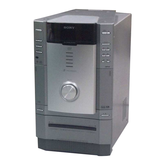
HCD-FL5D
Model Name Using Similar Mechanism
DVD Mechanism Type
DVD
Section
Base Unit Name
Optical Traverse Unit Name
Model Name Using Similar Mechanism
TAPE
Section
Tape Transport Mechanism Type
SPECIFICATIONS
Inputs
MD (VIDEO) IN:
(phono jacks)
voltage 450 mV/250 mV,
impedance 47 kilohms
OPTICAL DIGITAL IN:
(Square optical connector jacks, rear panel)
wavelength
——
MIC:
sensitivity 1 mV,
(phone jack)
impedance 10 kilohms
Outputs
MD (VIDEO) OUT:
(phono jacks)
voltage 250 mV
impedance 1 kilohms
VIDEO OUT:
1 Vp-p, 75 ohms
S-VIDEO OUT:
Y: 1 Vp-p, 75 ohms
C: 0.286Vp-p, 75 ohms
COMPONENT OUT:
Y: 1 Vp-p, 75 ohm
P
: 0.7 Vp-p, 75 ohms
B
P
: 0.7 Vp-p, 75 ohms
R
PHONES:
accepts headphones of
(stereo mini jack)
8 ohms or more
FRONT L/R:
Use only the supplied
speaker SS-FL7
REAR L/R:
Use only the supplied
speaker SS-RS7
CENTER:
Use only the supplied
speaker SS-CT7
S.WOOFER:
Use only the supplied
speaker SS-WG7
E Model
Australian Model
NEW
CDM53N-DVBU14
DVBU14
DBU-1
NEW
TCM-230AWR41CS/
230PWR41CS
DVD player section
Laser
Semiconductor laser
(DVD: λ=650 nm,
CD: λ=780 nm)
Emission duration:
continuous
Frequency response
DVD (PCM 48 kHz):
2 Hz – 22 kHz = (±1 dB)
CD: 2 Hz – 20 kHz =
(±1 dB)
Signal-to-noise ratio
More than 90 dB
Dynamic range
More than 90 dB
Video color system format
NTSC, PAL
OPTICAL DVD DIGITAL OUT
(Square optical connector jack, rear panel)
wavelength
660 nm
Tape player section
Recording system
4-track 2-channel stereo
Frequency response
50 – 13,000 Hz (±3 dB),
using Sony TYPE I
cassette
±0.15% W.Peak (IEC)
Wow and flutter
0.1% W.RMS (NAB)
±0.2% W.Peak (DIN)
– Continued on next page –
DVD DECK RECEIVER
Advertisement
Table of Contents

Related Manuals for Sony HCD-FL5D


Summary of Contents for Sony HCD-FL5D
-
Page 1: Specifications
HCD-FL5D SERVICE MANUAL E Model Australian Model Ver 1.5 2004.09 HCD-FL5D is the amplifier, DVD player, tape deck and tuner section in DHC-FL5D. Model Name Using Similar Mechanism DVD Mechanism Type CDM53N-DVBU14 Section Base Unit Name DVBU14 Optical Traverse Unit Name... - Page 2 LINE WITH MARK 0 ON THE SCHEMATIC DIAGRAMS AND IN THE PARTS LIST ARE CRITICAL TO SAFE OPERATION. REPLACE THESE COMPONENTS WITH SONY PARTS WHOSE PART NUMBERS APPEAR AS SHOWN IN THIS MANUAL OR IN SUPPLEMENTS PUB- LISHED BY SONY.
-
Page 3: Audio Tracks
HCD-FL5D This system can play the Playing a disc with MP3 following discs audio tracks Notes About MP3 Format of discs Disc logo • With formats other than ISO 9660 level 1, 2 and MP3 (MPEG 1 Audio Layer-3) is a standard... -
Page 4: Table Of Contents
HCD-FL5D TABLE OF CONTENTS SERVICING NOTES 8-14. Schematic Diagram – MB Board (3/5) – ....... 50 ..........6 8-15. Schematic Diagram – MB Board (4/5) – ....... 51 8-16. Schematic Diagram – MB Board (5/5) – ....... 52 GENERAL 8-17. Printed Wiring Boards – CHANGER Section – .... 54 Location of Controls ............ - Page 5 HCD-FL5D 9-16. Tape Mechanism Deck Section-2 (TCM-230PWR41CS: TH Model) ........ 129 9-17. Tape Mechanism Deck Section-3 (TCM-230PWR41CS: TH Model) ........ 130 10. ELECTRICAL PARTS LIST ......131...
-
Page 6: Servicing Notes
HCD-FL5D SECTION 1 SERVICING NOTES • MODEL IDENTIFICATION NOTES ON HANDLING THE OPTICAL PICK-UP – Back Panel – BLOCK OR BASE UNIT The laser diode in the optical pick-up block may suffer electro- static break-down because of the potential difference generated by the charged electrostatic load, etc. - Page 7 HCD-FL5D Ver 1.5 • RELEASING THE DISC TRAY LOCK NOTE OF REPLACING THE MB BOARD When replacing the MB board, since the adjustment value is not The disc tray lock function for the antitheft of an demonstration set up correctly, “Drive Auto Adjustment” can’t be performed.
-
Page 8: General
HCD-FL5D SECTION 2 This section is extracted from instruction manual. GENERAL LOCATION OF CONTROLS – Front Panel – E – R T – V ALPHABETICAL ORDER TAPE A/B ea ECHO LEVEL (Asian model only) wa TUNER/BAND es A – D... -
Page 9: Remote Control
HCD-FL5D Remote Control Setting the clock Turn on the system. ALPHABETICAL ORDER Press CLOCK/TIMER SET on the A – E F – S T – V remote. TAPE A/B qs 2.1CH/MULTI* e; FUNCTION 0 Press . or > repeatedly to set the ALBUM +/–... -
Page 10: Disassembly
HCD-FL5D SECTION 3 DISASSEMBLY • This set can be disassembled in the order shown below. 3-1. DISASSEMBLY FLOW 3-2. TOP PANEL ASSY (Page 11) 3-3. BACK COVER (Page 11) 3-4. SIDE PANEL (A)/(B) (Page 12) 3-5. CASE (Page 12) 3-6. FRONT PANEL ASSY (Page 13) 3-7. -
Page 11: Top Panel Assy
HCD-FL5D Note: Follow the disassembly procedure in the numerical order given. 3-2. TOP PANEL ASSY 1 four screws (hexagon socket tapping) 2 top panel assy 3-3. BACK COVER 1 five screws (BVTP3 × 8) 2 back cover... -
Page 12: Side Panel (A)/(B)
HCD-FL5D 3-4. SIDE PANEL (A) / (B) 2 side panel (B) 4 side panel (A) 3 three screws (top) 1 three screws (top) 3-5. CASE 3 screw (case 3 TP2) 5 two screws 2 six screws (BVTP3 × 8) (BVTT3 × 8 (S)) -
Page 13: Front Panel Assy
HCD-FL5D 3-6. FRONT PANEL ASSY 3 connector qg Rifting up the CD mechanism block 4 connector (CN203) 1 wire (flat type) (15 core) section, and release two claws. (CN207) (CN206) 2 connector (CN201) 8 connector (CN808) qs screw (BVTP3 × 8) -
Page 14: Tape Mechanism Assy
HCD-FL5D 3-8. TAPE MECHANISM ASSY 3 Push two solenoids. 1 two screws (2.6 × 8) 5 tape mechanism assy 4 Open cassette lid. 2 two screws 3-9. BELT 4 belt (capstan B) 2 motor assy (capstan) 3 belt (capstan C) -
Page 15: Sw Board, Head (A) Board, Head (B) Board
HCD-FL5D 3-10. SW BOARD, HEAD (A) BOARD, HEAD (B) BOARD 2 five claws 3 SW board 1 Remove the four solders. 5 head (A) board 7 head (B) board 4 screw (PTT 2 × 4) 6 screw (PTT 2 × 4) 3-11. -
Page 16: Dsp Board
HCD-FL5D 3-12. DSP BOARD 5 DSP board 3 wire (flat type) (11 core) 4 two screws (BVTP3 × 8) (CN601) 1 wire (flat type) (9 core) (CN603) 2 wire (flat type) (19 core) (CN602) 3-13. DVD MECHANISM DECK (CDM53N-DVBU14) 2 two screws (BVTP 3 ×... -
Page 17: Fitting Base (Guide) Assy, Bracket (Chassis), Magnet Assy
HCD-FL5D 3-14. FITTING BASE (GUIDE) ASSY, BRACKET (CHASSIS), MAGNET ASSY 8 four screws 6 Bracket (BTTP M2.6) (chassis) 2 four screws (BTTP M2.6) 4 two screws (BTTP M2.6) 7 connector (CN710) 9 magnet assy 5 two screws (BTTP M2.6) 3 fitting base... -
Page 18: Tray (Sub)
HCD-FL5D 3-16. TRAY (SUB) 1 Rotating the pulley (LD), shift the slider (selection) in the arrow A direction. 2 Rotating the pulley (mode) in the arrow direction, adjust the tray (sub) to be removed. 3 Rotating the pulley (LD), shift the slider (selection) in the arrow B direction. -
Page 19: Video Board
HCD-FL5D 3-18. VIDEO BOARD 2 video board 1 three screws (BVTP3 × 8) 3-19. SUB TRANS BOARD 1 connector (CN901) 3 three screws (BVTP3 × 8) 2 connector (CN902) 4 harness 5 SUB trans board... -
Page 20: Back Cover Section
HCD-FL5D 3-20. BACK COVER SECTION 4 two screws (BVTP3 × 8) 1 connector (CN902) 2 connector (CN809) 3 connector (CN901) 5 screw (BVTP3 × 8) 6 back cover section 3-21. TRANS BOARD 4 four screws 1 connector (CN914) 5 TRANS board... -
Page 21: Sp Relay Board
HCD-FL5D 3-22. SP RELAY BOARD 6 two connectors (CN801) 4 two connectors (CN803, 804) 7 SP relay board front rear AMP board 1 two screws (BVTP3 × 8) 5 two claws 2 screw (BVTP3 × 8) center SW AMP board... -
Page 22: Assembly
HCD-FL5D SECTION 4 ASSEMBLY • This set can be assembled in the order shown below. 4-1. ASSEMBLY FLOW 4-2. GEARS INSTALLATION (Page 22) 4-3. SLIDER (SELECTION) INSTALLATION (Page 23) 4-4. STOCKER SECTION INSTALLATION (Page 23) 4-5. CHASSIS (MOLD B) SECTION INSTALLATION (Page 24) Note: Follow the assembly procedure in the numerical order given. -
Page 23: Slider (Selection) Installation
HCD-FL5D 4-3. SLIDER (SELECTION) INSTALLATION 6 two screws (PTPWH M2.6) 2 gear (chuking) rotary encoder 5 washer 4 compression spring 7 Insert the slider (selection) into the portion A. Align with the slot of rotary encoder. portion A 3 convex portion of... -
Page 24: Chassis (Mold B) Section Installation
HCD-FL5D 4-5. CHASSIS (MOLD B) SECTION INSTALLATION 3 three screws (BVTP M2.6) 2 Insert the gear (eject) 1 Insert the portion A of under the gear (LD chassis (mold B) section deceleration). portion A into the portion B of slider (selection). -
Page 25: Test Mode
HCD-FL5D SECTION 5 TEST MODE [COLD RESET] OPEN/CLOSE DETECT” switch is turned on, “C” value in- creases. • The cold reset clears all data including preset data stored in the Each time the “CASSETTE LID OPEN/CLOSE DETECT” RAM to initial conditions. Execute this mode when returning switch is pressed, “T”... - Page 26 HCD-FL5D 4. Tape Recording Test [CD REPEAT 5 LIMIT OFF MODE] Procedure: Number of repeat for CD playback is 5 times when the repeat 1. Enter the MC Test Mode. mode is “REPEAT”. This mode enables CD to repeat playback for 2.
- Page 27 HCD-FL5D Ver 1.3 [DVD TEST MODE GENERAL DESCRIPTION] 0-1. All (All items continuous check) This menu checks all diagnostic items continuously. Normally, all The Test Mode allows you to make diagnosis and adjustment eas- items are checked successively one after another automatically un- ily using the remote commander and monitor TV.
- Page 28 HCD-FL5D 0-2. Version 1. DRIVE AUTO ADJUSTMENT 0-2-2. Revision On the Test Mode Menu screen, press the key on the remote The revision number of ROM (IC205 (TYPE A) or IC204 commander, and the Adjustment Menu will be displayed. (TYPE B)) that the program for the DVD system processor (IC206) is stored.
- Page 29 HCD-FL5D 2. DRIVE MANUAL OPERATION 2-1. Disc Type Note: This mode is used for design, and not used in service fundamen- tally. Disc Type On the Test Mode Menu screen, press the key on the remote Disc Type Select commander, and the Operation Menu will be displayed. For the manual operation, each servo on/off control and adjustment can 1.
- Page 30 HCD-FL5D 2-1-3. Disc Type CD 2-3. Track/Layer Jump It sets up so that it may judge as a disc type of specification of the disc with which the set was inserted. Track/Layer Jump : CD disc (normal speed, 12 cm) FWD R.Lj L0>L1...
- Page 31 HCD-FL5D 2-5. EEPROM Write Adjust 2-7. Disc Check Memory EEPROM Write Adjust Disc Check Memory 1. Focus Offset 1. SL Disc check 2. Focus Gain 2. SL Disc check 3. Trk. Offset Coarse 3. SL Disc check 4. —————— 5. Trk.
- Page 32 HCD-FL5D 3. MECHA AGING • Code list of Emergency History 10: Communication to RF AMP (IC001) failed. On the Test Mode Menu screen, selecting executes the aging 11: Each servo for focus, tracking, and spindle is unlocked. of the mechanism deck.
- Page 33 HCD-FL5D • Error code (aa) 6. VERSION INFORMATION FF : Complete the initializing. (normal operation) On the Test Mode Menu screen, selecting displays the ROM 11 : Stocker movement (to chucking position) failing in the midst version and region code.
-
Page 34: Mechanical Adjustments
HCD-FL5D SECTION 6 SECTION 7 MECHANICAL ADJUSTMENTS ELECTRICAL ADJUSTMENTS Precaution DECK SECTION 0 dB=0.775 V 1. Clean the following parts with a denatured alcohol-moistened swab: 1. Demagnetize the record/playback head with a head record/playback heads pinch rollers demagnetizer. erase head rubber belts 2. - Page 35 HCD-FL5D 3. Mode: Playback Mode: Playback SP RELAY board test tape test tape CN804 P-4-A100 WS-48B frequency counter oscilloscope Pin 2 (L-CH) (10 kHz, –10 dB) (3 kHz, 0 dB) pin 2 Pin 5 (R-CH) L-CH pin 3 – REALY...
- Page 36 HCD-FL5D Ver 1.5 – SW BOARD (Component Side) – REC LEVEL ADJUSTMENT DECK B TAPE SPEED ADJUSTMENT Procedure: In the MC test mode, the “REC memory mode” is convenient for (NORMAL) (HIGH) this adjustment. In the “REC memory mode” , when the REC starts the input signal FUNCTION is switched to VIDEO automatically.
-
Page 37: Diagrams
HCD-FL5D SECTION 8 DIAGRAMS 8-1. BLOCK DIAGRAM – RF SERVO Section – • SIGNAL PATH : CD PLAY CDDOUT (Page 39) : DVD PLAY : VIDEO 117 RFIN SD0 – SD7 (for AUDIO SYSTEM) (Page 41) DOUT AV DATA BUS... -
Page 38: Block Diagram - Tuner/Tape Deck Section
HCD-FL5D 8-2. BLOCK DIAGRAM – TUNER/TAPE DECK Section – TUNER UNIT ANTENNA TUNER L-CH (Page 39) FM ANT L-CH FM 75Ω ANT GND R-CH R-CH AM ANT ST-DOUT ANT GND ST-DIN ST-CLK ST-CE MUTING ST-MUTE TUNED TUNED STEREO DECK A/B SELECT SWITCH,... -
Page 39: Block Diagram - Audio Dsp Section
HCD-FL5D 8-3. BLOCK DIAGRAM – AUDIO DSP Section – TUNER L-CH • R-ch is omitted due • Abbreviation to same as L-ch. (Page 38) MX : Mexican • SIGNAL PATH TAPE J701 (1/2) L-CH : AUDIO : TAPE PLAY : REC... -
Page 40: Block Diagram - Power Amp Section
HCD-FL5D 8-4. BLOCK DIAGRAM – POWER AMP Section – J301 HP SW PHONES (Page 42) TM801 –2 FRONT L –2 – –1 –1 FRONT R (Page 39) – RY801 POWER AMP RELAY DRIVE IC401 Q801 R-CH –2 RY802 OVER LOAD –1... -
Page 41: Block Diagram - Video Section
HCD-FL5D 8-5. BLOCK DIAGRAM – VIDEO Section – • SIGNAL PATH : DVD PLAY : VIDEO VDAC_0 SD0 – SD7 (Page 37) AV DATA BUS VIDEO AMP, 75Ω DRIVER : CHROMA IC701 : COMPONENT VIDEO 6 YIN VDAC_2 YOUT XDCK, XSAK,... -
Page 42: Block Diagram - Display/Power Supply Section
HCD-FL5D 8-6. BLOCK DIAGRAM – DISPLAY/POWER SUPPLY Section – CD/DVD DOOR OPEN/CLOSE MOTOR DRIVE IC302 EVER+4V S702 (LID) PRTC_SW OUT1 M301 DOOR MOTOR+ (ON: When CD/DVD lid is close.) MOTOR D103, 104 CD/DVD DOOR OUT2 DRIVE DOOR MOTOR– OPEN/CLOSE S701 (MID OUT) -
Page 43: Note For Printed Wiring Boards And Schematic Diagrams
HCD-FL5D 8-7. NOTE FOR PRINTED WIRING BOARDS AND SCHEMATIC DIAGRAMS • Circuit Boards Location SP relay board Note on Printed Wiring Boards: Note on Schematic Diagram: front rear AMP board • X : parts extracted from the component side. • All capacitors are in µF unless otherwise noted. pF: µµF •... -
Page 44: Printed Wiring Board - Rf Board
HCD-FL5D 8-8. PRINTED WIRING BOARD – RF Board – • See page 43 for Circuit Boards Location. RF BOARD RF BOARD (COMPONENT SIDE) (CONDUCTOR SIDE) FLEXIBLE BOARD OPTICAL TRAVERSE UNIT (DBU-1) IC001 MB BOARD CN501 (Page 46) (11) (11) 1-684-822- 1-684-822- •... -
Page 45: Schematic Diagram - Rf Board
HCD-FL5D 8-9. SCHEMATIC DIAGRAM – RF Board – • • See page 53 for Waveforms. See page 90 for IC Block Diagram. RFMON C006 C028 C027 R026 C013 C031 1000p CN002 C030 0.01 C026 AGND C025 R023 C029 RFAC 0.01... -
Page 46: Printed Wiring Board - Mb Board (Component Side)
HCD-FL5D 8-10. PRINTED WIRING BOARD – MB Board (Component Side) – • See page 43 for Circuit Boards Location. • Semiconductor Location Ref. No. Location MB BOARD D201 B-10 (COMPONENT SIDE) IC206 F-10 IC215 IC509 IC701 IC901 IC902 IC904 IC906... -
Page 47: Printed Wiring Board - Mb Board (Conductor Side)
HCD-FL5D Ver 1.2 8-11. PRINTED WIRING BOARD – MB Board (Conductor Side) – • Note: When replacing IC205 of type A, install IC204 instead of IC205. See page 43 for Circuit Boards Location. • Semiconductor Location Ref. No. Location MB BOARD... -
Page 48: Schematic Diagram - Mb Board (1/5)
HCD-FL5D 8-12. SCHEMATIC DIAGRAM – MB Board (1/5) – • • See page 53 for Waveforms. See page 90 for IC Block Diagram. (1/5) AGND A3V-1 DGND (Page 50) M12V MGND C526 C527 C522 0.01 FL502 R536 DSP_BUS R569 WAVRB... -
Page 49: Schematic Diagram - Mb Board (2/5)
HCD-FL5D 8-13. SCHEMATIC DIAGRAM – MB Board (2/5) – • See page 53 for Waveforms. (2/5) JITOFF RF_AC FL705 R726 100k R700 R725 C721 TP701 TP703 8.2k 1.8k R727 3.3k C715 0.0015 R545 R544 R540 R550 R724 100k 100k R714... -
Page 50: Schematic Diagram - Mb Board (3/5)
HCD-FL5D 8-14. SCHEMATIC DIAGRAM – MB Board (3/5) – • • See page 53 for Waveforms. See page 90 for IC Block Diagrams. (Page 49) (3/5) DOUT 768FS XRST_CD XRST_DVD I2C_SCL I2C_SIO LDSEL Q901 A3V-2 DTC114TE-TL R901 LASER DIODE FL901... -
Page 51: Schematic Diagram - Mb Board (4/5)
HCD-FL5D 8-15. SCHEMATIC DIAGRAM – MB Board (4/5) – • See page 53 for Waveforms. (4/5) CN204 C228 R272 R273 R274 R275 R276 VGND 0.01 VMUTE C225 C229 C230 C231 C232 C233 R250 0.01 0.01 0.01 0.01 0.01 R_GND R271... -
Page 52: Schematic Diagram - Mb Board (5/5)
HCD-FL5D Ver 1.2 8-16. SCHEMATIC DIAGRAM – MB Board (5/5) – Note: When replacing IC205 of type A, install IC204 instead of IC205. (5/5) MD15 FL202 FL203 C217 C257 C258 0.01 0.01 MD14 C219 C253 0.01 0.01 MD13 HA17 (TYPE A) - Page 53 HCD-FL5D • Waveforms – MB Board – – RF Board – 1 IC001 1 (DVDRFP) qa IC509 0 (WFCK) qh IC509 yj (BCK) wa IC701 <znc (LRCK) wh IC906 3 (MO1) ea IC206 <zx, (VDAC 1) (NTSC Color Bars Play) Approx.
-
Page 54: Printed Wiring Boards - Changer Section
HCD-FL5D 8-17. PRINTED WIRING BOARDS – CHANGER Section – • See page 43 for Circuit Boards Location. CLAMP MOTOR BOARD INIT/COUNT SW BOARD SENSOR 2 BOARD OUT/MIDOUT SW BOARD S702 (LID) ON : WHEN CD LID IS CLOSE (11) 1-683-900-... -
Page 55: Schematic Diagram - Changer Section
HCD-FL5D 8-18. SCHEMATIC DIAGRAM – CHANGER Section – • See page 90 for IC Block Diagrams. D704 GL528VS1 CN708 CN702 DISC IN DETECT R711 SENSOR R707 R709 2.2k Q701 RT1N141 R708 LEVEL SHIFT S702 (LID) (ON:WHEN CD/DVD LED IS CLOSE.) -
Page 56: Printed Wiring Boards - Cd Door Section
HCD-FL5D 8-19. PRINTED WIRING BOARDS – CD DOOR Section – • See page 43 for Circuit Boards Location. • Semiconductor Location Ref. No. Location CD DOOR BOARD CD MOTOR BOARD D341 D342 D343 D344 D345 R340 IC302 DISC 1 CD DOOR... -
Page 57: Schematic Diagram - Cd Door Section
HCD-FL5D 8-20. SCHEMATIC DIAGRAM – CD DOOR Section – • See page 90 for IC Block Diagram. (Page 79) CN309 S341 R341 ROTARY ENCODER VOLUME C341 C342 C343 (CHASSIS) CN317 CN312 VOL 1A CN313 NO814 VOL 1B D345 D344 D343... -
Page 58: Printed Wiring Board - Sw Board
HCD-FL5D 8-21. PRINTED WIRING BOARD – SW Board – • See page 43 for Circuit Boards Location. • Semiconductor Location M901 Ref. No. Location PM902 (CAPSTAN) D1001 (DECK B) PM901 D1002 B-10 (DECK A) IC1001 IC1002 IC1002 Q1001 IC1001 (DECK B PLAY) -
Page 59: Schematic Diagram - Sw Board
HCD-FL5D 8-22. SCHEMATIC DIAGRAM – SW Board – (CAPSTAN) C1001 CAPSTAN MOTOR CONTROL SWITCH TAPE SPEED (NORMAL) TAPE SPEED (HIGH) [∗] {2.9} <<2.9>> [3.3] [3.3] PM902 PM901 (DECK B) (DECK A) ROTATION ROTATION CAPM− DETECT DETECT SENSOR (DECK A) SENSOR (DECK B) -
Page 60: Printed Wiring Boards - Tc Door Section
HCD-FL5D 8-23. PRINTED WIRING BOARDS – TC DOOR Section – • See page 43 for Circuit Boards Location. TC DOOR SW BOARD TC SW(A) BOARD S325 CASSETTE LID OPEN/CLOSE DETECT NO809B (13) (13) TC DOOR BOARD GC BOARD CN203 (Page 78) -
Page 61: Schematic Diagram - Tc Door Section
HCD-FL5D 8-24. SCHEMATIC DIAGRAM – TC DOOR Section – S326 R338 NO810 CN319 2.2k NO813 KEYS RTN D GND TC DOOR SW JR214 SOLENOID A D309 D310 1SS355 1SS355 SOLENOID B CP302 CP304 M/LED GND (Page 79) S325 CP301 CP303... -
Page 62: Printed Wiring Board - Mc Board
HCD-FL5D Ver 1.2 8-25. PRINTED WIRING BOARD – MC Board – • See page 43 for Circuit Boards Location. • Semiconductor Location Ref. No. Location ANTENNA D101 D102 75Ω D103 D104 D105 D202 ∗ SUPPLIED WITH ∗ D203 TUNER PACK... -
Page 63: Schematic Diagram - Mc Board
HCD-FL5D Ver 1.2 8-26. SCHEMATIC DIAGRAM – MC Board – • See page 69 for Waveforms. (Page 50) CN112 ∗ SUPPLIED WITH R272 R273 THE ASSEMBLED CN105 BLOCK ST-MUTE R OUT A GND L OUT EP201 C242 STEREO JW236 ∗... -
Page 64: Printed Wiring Board - Dsp Board (Component Side)
HCD-FL5D 8-27. PRINTED WIRING BOARD – DSP Board (Component Side) – • See page 43 for Circuit Boards Location. • Semiconductor Location Ref. No. Location IC601 DSP BOARD (COMPONENT SIDE) IC603 IC611 IC612 IC701 F-10 IC702 IC703 IC704 Q790 C642... -
Page 65: Printed Wiring Board - Dsp Board (Conductor Side)
HCD-FL5D 8-28. PRINTED WIRING BOARD – DSP Board (Conductor Side) – • See page 43 for Circuit Boards Location. • Semiconductor Location Ref. No. Location D601 D-12 DSP BOARD (CONDUCTOR SIDE) D606 D611 D612 D741 D742 IC602 E-11 IC621 IC622... -
Page 66: Schematic Diagram - Dsp Board (1/3)
HCD-FL5D 8-29. SCHEMATIC DIAGRAM – DSP Board (1/3) – • See page 69 for Waveforms. (1/3) CN602 JR617 SPDIF(DVD) D+4V SPDIF(CD) JR616 D-GND(DSP) (Page 67) DSP-CS DSP-ACK DIR-Rx R614 C608 0.001 DIR_INT (Page 63) DIR-CS DIR-UNLOCK R613 DIG-CLK JR655 DSP-Rx... -
Page 67: Schematic Diagram - Dsp Board (2/3)
HCD-FL5D 8-30. SCHEMATIC DIAGRAM – DSP Board (2/3) – MD(VIDEO) J701 (CHASSIS GND) (2/3) FB702 R703 R753 C741 R701 R751 C704 C754 220p 220p (EXCEPT AUS) (AUS) R754 C702 C752 100k FB710 220p 220p R704 JR710 100k R702 R752 CN601... -
Page 68: Schematic Diagram - Dsp Board (3/3)
HCD-FL5D 8-31. SCHEMATIC DIAGRAM – DSP Board (3/3) – • • See page 69 for Waveforms. See page 90 for IC Block Diagrams. (Page 67) (3/3) R657 1.5k JR623 R656 R654 C662 C659 C663 C648 R653 R652 R651 0.001 (AUS) - Page 69 HCD-FL5D • Waveforms – SP RELAY Board – – MC Board – – DSP Board – – VIDEO Board – ra Q4, Q5 (Base) (REC Mode) ta IC101 qa (XC-OUT) ya IC601 qs (MCLK2) yh IC611 qf (BCK) ia IC701 qk, ql (CR OUT)
-
Page 70: Printed Wiring Board - Center Sw Amp Board
HCD-FL5D 8-32. PRINTED WIRING BOARD – CENTER SW AMP Board – • See page 43 for Circuit Boards Location. • Semiconductor Location CENTER SW AMP BOARD Ref. No. Location D501 D502 D551 D552 D591 D921 TRANS BOARD CN916 (Page 88) -
Page 71: Schematic Diagram - Center Sw Amp Board
HCD-FL5D 8-33. SCHEMATIC DIAGRAM – CENTER SW AMP Board – NO702 AC2(VH) POWER AMP AC2(VH) IC501 AC GND STK442-130 AC GND AC2(VH) D591 D591 D15XB20 RECT AC2(VH) AC3(MOTOR) (Page 89) C593 C591 R591 2200 AC3(MOTOR) 100k 100V C594 C592 C551... -
Page 72: Front Rear Amp Board
HCD-FL5D 8-34. PRINTED WIRING BOARD – FRONT REAR AMP Board – • See page 43 for Circuit Boards Location. SP RELAY BOARD (Page 74) CN801 FRONT REAR AMP BOARD (MX) TRANS BOARD CN915 (Page 88) IC401 IC431 (12) 1-684-260- DSP BOARD... -
Page 73: Schematic Diagram - Front Rear Amp Board
HCD-FL5D 8-35. SCHEMATIC DIAGRAM – FRONT REAR AMP Board – POWER AMP IC401 STK402-070S R455 NO701 0.22 C455 C456 R460 AC1(VL) AC1(VL) AC-GND R457 R456 0.22 AC-GND D491 D15XB20 AC1(VL) AC1(VL) R454 (Page 89) C451 R451 R458 R421 2.2k C493... -
Page 74: Printed Wiring Boards - Speaker Section
HCD-FL5D 8-36. PRINTED WIRING BOARDS – SPEAKER Section – • See page 43 for Circuit Boards Location. • Semiconductor Location REGULATOR BOARD Ref. No. Location IC801 IC802 IC803 IC804 D801 D802 MC BOARD (Page 62) MC BOARD (Page 62) CN102... -
Page 75: Schematic Diagram - Regulator Board
HCD-FL5D 8-37. SCHEMATIC DIAGRAM – REGULATOR Board – IC801 µPC3504AHF C870 C878 +4V REGULATOR IC802 TA7805S C871 C879 NO704 +5V REGULATOR IC803 TA7810S C872 C880 +10V REGULATOR (Page 77) IC804 TA7805S C873 C881 +5V REGULATOR Q864 2SB1375 R872 2.7k R871 R873 2.7k... -
Page 76: Schematic Diagram - Speaker Section (1/2)
HCD-FL5D 8-38. SCHEMATIC DIAGRAM – SPEAKER Section (1/2) – • See page 69 for Waveforms. (1/2) DVD+12V CD/DVD POWER M-GND M+9V UNREG-GND NO816 UNREG(M) A-GND 0.0022 M+12V (Page 71) PB-R 1 50V C844 M+12V C854 4.7k R889 0.01 REC-R 10 50V... -
Page 77: Schematic Diagram - Speaker Section (2/2)
HCD-FL5D 8-39. SCHEMATIC DIAGRAM – SPEAKER Section (2/2) – (Page 73) (Page 89) CN803 OVERLOAD STK MUTE POWER GND POWER GND CN801 NO703 CENTER GND CENTER GND R815 C815 CENTER (2/2) 100V CENTER SW GND C823 (Page 71) R885 0.01... -
Page 78: Printed Wiring Board - Gc Board
HCD-FL5D 8-40. PRINTED WIRING BOARD – GC Board – • See page 43 for Circuit Boards Location. • Semiconductor Location Ref. No. Location GC BOARD D201 D202 FLUORESCENT INDICATOR TUBE D203 D204 IC201 IC202 Q201 Q202 Q203 Q204 Q205 Q206... -
Page 79: Schematic Diagram - Gc Board
HCD-FL5D 8-41. SCHEMATIC DIAGRAM – GC Board – • See page 69 for Waveform. FL201 FLUORESCENT INDICATOR TUBE EP202 C209 C221 (CHASSIS) CN201 D204 1SS355 EVER+3.3V C210 LED A LED B Q212 2SC2785 Q203-206,212 LED GND C223 LED DRIVE LED5... -
Page 80: Printed Wiring Boards - Panel Section
HCD-FL5D 8-42. PRINTED WIRING BOARDS – PANEL Section – • See page 43 for Circuit Boards Location. PANEL (L) BOARD D301, S301 D304, S305 IC301 DIGITAL MD (VIDEO) TAPE A/B DISPLAY D302, S303 D303, S304 TUNER/BAND (13) 1-684-192- BLUE LED BOARD... -
Page 81: Schematic Diagram - Panel Section
HCD-FL5D 8-43. SCHEMATIC DIAGRAM – PANEL Section – R321 R322 R323 R324 R325 R326 R327 R328 1.5k 1.5k 2.2k 3.3k 4.7k 6.8k S311 S312 S313 S314 S315 S316 S317 S318 S319 D304 D303 D302 D301 SELS5923C SELS5923C SELS5923C SEL5223S NO812... -
Page 82: Printed Wiring Board - Mic Board
HCD-FL5D 8-44. PRINTED WIRING BOARD – MIC Board – • See page 43 for Circuit Boards Location. MIC BOARD (EXCEPT MX) C373 R366 C380 C368 C367 C376 R369 R370 C378 C375 R375 IC352 R371 R372 RV352 C370 C372 ECHO LEVEL... -
Page 83: Schematic Diagram - Mic Board
HCD-FL5D 8-45. SCHEMATIC DIAGRAM – MIC Board – • See page 90 for IC Block Diagram. C360 R358 100p 150k MIC AMP IC351(2/2) C358 IC351(1/2) C351 C361 NJM4580E-D(T1) C356 R357 NJM4580E-D(T1) R352 0.22 R359 C359 C355 J351 R356 R355 C357 ∗... -
Page 84: Printed Wiring Board - Video Board
HCD-FL5D 8-46. PRINTED WIRING BOARD – VIDEO Board – • See page 43 for Circuit Boards Location. • Semiconductor Location Ref. No. Location IC701 MB BOARD CN204 Q711 Q712 (Page 46) VIDEO BOARD IC701 JW780 JW785 JW784 C784 C782 C780... -
Page 85: Schematic Diagram - Video Board
HCD-FL5D 8-47. SCHEMATIC DIAGRAM – VIDEO Board – • • See page 69 for Waveforms. See page 90 for IC Block Diagram. CN701 VIDEO AMP, 75W DRIVER VGND IC701 J701 VMUTE1 MM1568 R722 R_GND C751 22 50V FB717 R702 GND2... -
Page 86: Printed Wiring Board - Sub Trans Board
HCD-FL5D 8-48. PRINTED WIRING BOARD – SUB TRANS Board – • See page 43 for Circuit Boards Location. • Semiconductor Location Ref. No. Location SUB TRANS BOARD D901 D902 S901 D903 D904 VOLTAGE SELECTOR D905 120V 220V 230 − 240V (SP) D906 120V −... -
Page 87: Schematic Diagram - Sub Trans Board
HCD-FL5D 8-49. SCHEMATIC DIAGRAM – SUB TRANS Board – (EA,SP) JW911 ∗ CN902 JW912 (EXCEPT EA,SP) (EA,SP) (TH, AUS) (EA,SP) JW913 CN902 ∗ F913 (EXCEPT EA,SP) T5AL 250V JW907 (EA,MX,SP) (Page 89) JW906 (EXCEPT EA,SP) (EA,SP) R904 (EA,SP) R901 S901... -
Page 88: Printed Wiring Board - Trans Board
HCD-FL5D 8-50. PRINTED WIRING BOARD – TRANS Board – • See page 43 for Circuit Boards Location. TRANS BOARD R912 JW928 (AUS) SP RELAY BOARD NO703 T911 (Page 74) MAIN POWER TRANSFORMER (TH) SUB TRANS BOARD CN902 (Page 86) (EA, MX, SP) -
Page 89: Schematic Diagram - Trans Board
HCD-FL5D 8-51. SCHEMATIC DIAGRAM – TRANS Board – CN915 AC1(VL) AC1(VL) AC GND AC GND AC1(VL) F916 AC1(VL) (Page 73) T8AL 250V (AUS) ∗ JW921 (EXCEPT EA,SP) F914 T911 (EA,SP) T8AL MAIN 250V (TH) POWER (EA,SP) TRANSFORMER JW922 CN916 F915 ∗... - Page 90 HCD-FL5D • IC Block Diagrams – RF Board – – MB Board – IC001 CXD1881AR IC215 SN74ALVCH16841DGGR 56 1LE 64 63 62 61 60 59 55 54 53 52 FAST ATTACK INPUT OUTPUT FULL WAVE AGC CHARGE HOLD INHIBIT RECTIFER...
- Page 91 HCD-FL5D IC509 CXD3068Q 59 58 57 56 55 54 53 52 51 50 49 48 47 46 45 44 43 42 41 DVDD2 ASYE DIGITAL ASYMMETRY CORRECTOR DIGITAL DOUT LRCK D/A DIGITAL PCMD INTERFACE DEMODULATOR TES1 TEST1 ERROR DVSS1 CORRECTOR...
- Page 92 HCD-FL5D IC706 MSM51V18165F-60TSKR1 40 – 36 34 33 REFRESH INTERNAL TIMING CONTROL ADDRESS GENERATOR CLOCK COUNTER CONTROLLER OUTPUT INPUT BUFFER BUFFER COLUMN CONTROLLER ADDRESS ADDRESS BUFFERS BUFFERS SENSE COLUMN AMPLIFIER DECODERS OUTPUT INPUT BUFFER BUFFER MEMORY WORD CELLS DECODERS DRIVERS...
- Page 93 HCD-FL5D – CLAMP MOTOR Board – IC701 BA6956AN CONTROL LOGIC – LOADING MOTOR Board – IC702 BA6956AN CONTROL LOGIC – CD MOTOR Board – IC302 BA6956AN CONTROL LOGIC...
- Page 94 HCD-FL5D – DSP Board – IC603 LC89057W-VF4-E MODULATOR MICROCONTROLLER & INTERFACE PARALLEL PORT RERR RXOUT CKST AUDIO/VO C bit, U bit EMPHA/UO 31 DGND DATA INPUT DEMODULATOR DVDD SELECTOR DATA & DGND SELECTOR LOCK DETECT DVDD RX5/V1 RX6/U1 XOUT XMCK...
- Page 95 HCD-FL5D IC612 PCM1608Y/2K 32 31 30 36 35 34 33 VCC3 FUNCTION AGND3 CONTROL VCC4 INTERFACE AGND4 SYSTEM SCKI CLOCK SCKO MANAGER VOUT8 AGND6 VCC5 LRCK AGND5 TEST ENHANCED 4X/8X VOUT7 OVER SAMPLING MULTI- SERIAL DIGITAL LEVEL INPUT DELTA- FILTER...
- Page 96 HCD-FL5D – VIDEO Board – IC701 MM1568 VCC1 VCC2 BIAS 75Ω COUT DRIVER MUTE1 CLAMP GND2 75Ω VOUT DRIVER YC MIX VSAG CLAMP GND2 75Ω YOUT DRIVER BIAS BIAS YSAG GND1 GND1 10 NC 11 GND2 CYIN 12 75Ω CYOUT...
-
Page 97: Ic Pin Function Description
HCD-FL5D 8-52. IC PIN FUNCTION DESCRIPTION • MB BOARD IC509 CXD3068Q (DIGITAL SIGNAL PROCESSOR, DIGITAL SERVO PROCESSOR) Pin No. Pin Name Description DVDD0 — Power supply terminal (+3.3V) (digital system) XRST Reset signal input from the mechanism controller “L”: reset MUTE Muting on/off control signal input from the mechanism controller “H”: muting on... - Page 98 HCD-FL5D Pin No. Pin Name Description AVDD0 — Power supply terminal (+3.3V) (analog system) ASYO EFM full-swing output terminal ASYI Asymmetry comparator voltage input terminal RFAC EFM signal input from the DVD/CD RF amplifier AVSS1 — Ground terminal (analog system)
- Page 99 HCD-FL5D • MB BOARD IC701 CXD1882R (DVD DECODER) Pin No. Pin Name Description 1, 2 D5, D6 Two-way data bus with the mechanism controller — Ground terminal (digital system) Two-way data bus with the mechanism controller Address signal input from the mechanism controller —...
- Page 100 HCD-FL5D Pin No. Pin Name Description XSRQ Serial data request signal input from the DVD system processor HINT Not used XS16 Not used Not used XPDI Not used VDDS — Power supply terminal (+5V) (digital system) 59, 60 HA0, HA2 Not used —...
- Page 101 HCD-FL5D Pin No. Pin Name Description RFDCC Input terminal for adjusting DC cut high-pass filter for RF signal Not used RFIN RF signal input from the DVD/CD RF amplifier 118, 119 VCCA5, VCCA4 — Power supply terminal (+3.3V) (analog system) VCOR1 —...
- Page 102 HCD-FL5D Pin No. Pin Name Description XTAL 33.8688 MHz clock signal input terminal — Ground terminal (digital system) XTA2 System clock output terminal (33.8688 MHz) XTA1 System clock input terminal (33.8688 MHz) — Power supply terminal (+3.3V) (digital system) 172 to 176...
- Page 103 HCD-FL5D • MB BOARD IC901 CXP973064-224R (MECHANISM CONTROLLER) Pin No. Pin Name Description EEP SO Not used SDEN Serial data enable signal output to DVD/CD RF amplifier DOCTRL/ Digital out on/off control signal output to the digital signal processor ISBTEST “L”: digital out off, “H”: digital out on...
- Page 104 HCD-FL5D Pin No. Pin Name Description MUTE DSD Muting on/off control signal output terminal “H”: muting on Not used SQCK Subcode Q data reading clock signal output to the digital signal processor — Ground terminal (digital system) TRAY IN Disc tray in detection signal input terminal Not used...
- Page 105 HCD-FL5D • MC BOARD IC101 M30622MGN-B06FP (SYSTEM CONTROLLER) Pin No. Pin Name Description AMP-DATA Serial data output to the M61520FP AMP-CLK Serial data transfer clock signal output to the M61520FP AMP-LAT Serial data latch pulse signal output to the M61520FP...
- Page 106 HCD-FL5D Pin No. Pin Name Description Serial data latch pulse output terminal Not used XRST Reset signal output to the DVD system processor “L”: reset VIDEO-MUTE, 44, 45 Video muting on/off control signal output terminal “L”: muting on VIDEO-MUTE2 NO-USE —...
- Page 107 HCD-FL5D Pin No. Pin Name Description Automatic limiter control signal output “H”: limiter on DIR-RST Reset signal output to the digital audio interface receiver SW phase control signal output terminal A-SHUT Shut off detection signal input from the deck-A side reel pulse detector...
- Page 108 HCD-FL5D • DSP BOARD IC601 CXD9720Q (AUDIO DIGITAL SIGNAL PROCESSOR) Pin No. Pin Name Description — Ground terminal XRST Reset signal input from the digital audio interface receiver “L”: reset EXTIN Master clock signal input terminal Not used LRCKI3 L/R sampling clock signal input from the A/D converter or digital audio interface receiver VDDI —...
- Page 109 HCD-FL5D Pin No. Pin Name Description — Ground terminal WMD0 S-RAM wait mode setting terminal Fixed at “L” in this set PAGE2 Page selection signal output terminal Not used — Ground terminal PAGE1, PAGE0 52, 53 Page selection signal output terminal Not used...
- Page 110 HCD-FL5D Pin No. Pin Name Description Synchronous/asychronous selection signal input terminal SYNC “L”: Synchronous, “H”: asynchronous (fixed at “H” in this set) TST2 — Ground terminal GP11 — Not used TST3 — Ground terminal VDDI — Power supply terminal (+3.3V)
- Page 111 HCD-FL5D • GC BOARD IC201 MB90M407PF-G-123-BND (FLUORESCENT INDICATOR TUBE DRIVER, KEY CONTROL, CD/DVD MECHANISM DECK CONTROLLER) Pin No. Pin Name Description 1 to 8 G17 to G24 Grid drive signal output to the fluorescent indicator tube 9, 10 A36, 35 —...
- Page 112 HCD-FL5D Pin No. Pin Name Description VSS-(CPU) — Ground terminal (for CPU) System clock input terminal (4 MHz) System clock output terminal (4 MHz) VCC-(CPU) — Power supply terminal (+3.3V) (for CPU) 85 to 100 G1 to G16 Grid drive signal output to the fluorescent indicator tube...
- Page 113 HCD-FL5D • GC BOARD IC202 PT8300 (FRONT PANEL CONTROLLER) Pin No. Pin Name Description — Ground terminal RESET_B Reset signal input from the system controller Serial data transfer clock signal input from the fuluorescent indicator driver LATCH Serial data latch pulse input from the fuluorescent indicator driver...
-
Page 114: Exploded Views
HCD-FL5D SECTION 9 EXPLODED VIEWS NOTE: • -XX and -X mean standardized parts, so they • Items marked “*” are not stocked since they The components identified by mark 0 or dotted line with mark 0 are may have some difference from the original are seldom required for routine service. -
Page 115: Front Panel Section-1
HCD-FL5D 9-2. FRONT PANEL SECTION-1 not supplied TCM-230AWR41CS/ TCM-230PWR41CS front panel section-2 Ref. No. Part No. Description Remark Ref. No. Part No. Description Remark 4-240-965-01 SCREW 2.6X3 +P, S-TITE 4-951-620-01 SCREW (2.6X8), +BVTP 4-215-062-01 DAMPER 7-685-853-04 SCREW +BVTT 2X6 (S) -
Page 116: Front Panel Section-2
HCD-FL5D 9-3. FRONT PANEL SECTION-2 not supplied M301 not supplied not supplied front panel section-3 Ref. No. Part No. Description Remark Ref. No. Part No. Description Remark 4-951-620-01 SCREW (2.6X8), +BVTP 1-773-032-11 WIRE (FLAT TYPE) (15 CORE) 1-684-200-11 TC SW (A) BOARD 1-684-204-11 CD DOOR SW1 BOARD 4-957-577-01 SCREW PTP WH (2.6X8) (DIA. -
Page 117: Front Panel Section-3
HCD-FL5D 9-4. FRONT PANEL SECTION-3 front panel section-4 supplied with S341 not supplied not supplied Ref. No. Part No. Description Remark Ref. No. Part No. Description Remark 1-684-205-11 CD DOOR SW2 BOARD 1-684-203-11 CD DOOR BOARD X-4954-585-1 BRACKET (PANEL PANEL, MOVING) ASSY 4-951-620-01 SCREW (2.6X8), +BVTP... -
Page 118: Front Panel Section-4
HCD-FL5D 9-5. FRONT PANEL SECTION-4 supplied with J351 not supplied Ref. No. Part No. Description Remark Ref. No. Part No. Description Remark 4-238-994-01 KNOB (MIC) X-4954-686-4 PANEL ASSY, FRONT (AUS, EA, SP) 4-951-620-01 SCREW (2.6X8), +BVTP X-4954-770-4 PANEL ASSY, FRONT (MX) -
Page 119: Chassis Section-1
HCD-FL5D Ver 1.2 9-6. CHASSIS SECTION-1 not supplied CDM53N-DVBU14 IC802 IC803 IC801 IC804 not supplied supplied chassis section-2 Ref. No. Part No. Description Remark Ref. No. Part No. Description Remark 1-765-324-11 WIRE (FLAT TYPE) (11 CORE) 1-684-271-11 REGULATOR BOARD 1-824-686-11 WIRE (FLAT TYPE) (13 CORE) -
Page 120: Chassis Section-2
HCD-FL5D 9-7. CHASSIS SECTION-2 EA, MX, SP F913 T911 F919 F918 F916 F915 F914 F917 chassis section-3 The components identified by mark 0 or dotted line with mark 0 are critical for safety. Replace only with part number specified. Ref. No. -
Page 121: Chassis Section-3
HCD-FL5D 9-8. CHASSIS SECTION-3 not supplied not supplied not supplied IC921 IC922 supplied chassis section-4 Ref. No. Part No. Description Remark Ref. No. Part No. Description Remark 3-970-608-01 SUMITITE (B3), +BV A-4730-387-A FRONT REAR AMP BOARD, COMPLETE (MX) A-4676-827-A CENTER SW AMP BOARD, COMPLETE... -
Page 122: Chassis Section-4
HCD-FL5D 9-9. CHASSIS SECTION-4 not supplied M801 not supplied The components identified by mark 0 or dotted line with mark 0 are critical for safety. Replace only with part number specified. Ref. No. Part No. Description Remark Ref. No. Part No. -
Page 123: Dvd Mechanism Deck Section-1 (Cdm53N-Dvbu14)
HCD-FL5D 9-10. DVD MECHANISM DECK SECTION-1 (CDM53N-DVBU14) not supplied supplied not supplied supplied mechanism deck section-3 supplied supplied mechanism deck section-2 Ref. No. Part No. Description Remark Ref. No. Part No. Description Remark 4-218-253-11 SCREW (M2.6), +BTTP 4-964-461-02 HOLDER (SENSOR) 3-341-549-01 SCREW (2.6X12) (DIA.7.5),+PTP WH... -
Page 124: Dvd Mechanism Deck Section-2 (Cdm53N-Dvbu14)
HCD-FL5D 9-11. DVD MECHANISM DECK SECTION-2 (CDM53N-DVBU14) M702 Ref. No. Part No. Description Remark Ref. No. Part No. Description Remark 4-218-253-11 SCREW (M2.6), +BTTP 4-211-232-01 GEAR (LD DECELERATION) 1-683-902-11 LOADING MOTOR BOARD 4-211-228-01 LEVER (GOOSENECK) 4-211-235-01 BELT (COMMUNICATION) 4-214-130-01 GEAR (TRAY) -
Page 125: Dvd Mechanism Deck Section-3 (Cdm53N-Dvbu14)
HCD-FL5D 9-12. DVD MECHANISM DECK SECTION-3 (CDM53N-DVBU14) not supplied mechanism deck section-4 not supplied base unit section (DVBU14) Ref. No. Part No. Description Remark Ref. No. Part No. Description Remark 4-985-672-01 SCREW (+PTPWH M2.6), FLOATING 4-933-134-01 SCREW (M2.6), +PTPWH 4-211-234-01 BRACKET (STOCKER T) -
Page 126: Dvd Mechanism Deck Section-4 (Cdm53N-Dvbu14)
HCD-FL5D 9-13. DVD MECHANISM DECK SECTION-4 (CDM53N-DVBU14) not supplied S707 not supplied M701 Ref. No. Part No. Description Remark Ref. No. Part No. Description Remark 4-218-253-11 SCREW (M2.6), +BTTP 4-211-221-01 GEAR (LD MOVABLE) 1-683-901-11 CLAMP MOTOR BOARD 4-211-242-11 SHAFT (SELECTION GEAR) -
Page 127: Base Unit Section (Dvbu14)
HCD-FL5D Ver 1.4 9-14. BASE UNIT SECTION (DVBU14) The components identified by mark 0 or dotted line with mark 0 are critical for safety. Replace only with part number specified. Ref. No. Part No. Description Remark Ref. No. Part No. -
Page 128: Tape Mechanism Deck Section-1 (Tcm-230Awr41Cs: Except Th Model)
HCD-FL5D 9-15. TAPE MECHANISM DECK SECTION-1 (TCM-230AWR41CS: EXCEPT TH MODEL) M901 HP901 supplied not supplied HRPE901 not supplied Ref. No. Part No. Description Remark Ref. No. Part No. Description Remark X-3374-156-5 PINCH LEVER (REV) ASSY X-3378-043-1 FLYWHEEL (B-REV) ASSY X-3374-155-5 PINCH LEVER (FWD) ASSY... -
Page 129: Tape Mechanism Deck Section
HCD-FL5D 9-16. TAPE MECHANISM DECK SECTION-2 (TCM-230PWR41CS: TH MODEL) PM901 HP901 PM902 HRPE901 tape mechanism deck section-3 Ref. No. Part No. Description Remark Ref. No. Part No. Description Remark 3-016-574-11 SPRING (HEAD), TENSION A-4728-872-A SW BOARD, COMPLETE 3-017-366-01 BASE (PINCH LEVER REV) - Page 130 HCD-FL5D 9-17. TAPE MECHANISM DECK SECTION-3 (TCM-230PWR41CS: TH MODEL) M901 Ref. No. Part No. Description Remark Ref. No. Part No. Description Remark 3-041-946-11 BELT (CAPSTAN B) 3-019-208-01 WASHER, STOPPER 4-227-239-11 BELT (CAPSTAN C) 3-040-580-02 PULLEY (TENSION) X-3378-249-1 FLYWHEEL (B-FWD) ASSY...
-
Page 131: Electrical Parts List
HCD-FL5D SECTION 10 ELECTRICAL PARTS LIST BLUE LED CD DOOR CD DOOR SW1 CD DOOR SW2 CD MOTOR NOTE: • Due to standardization, replacements in the • Items marked “*” are not stocked since they The components identified by parts list may be different from the parts speci- are seldom required for routine service. - Page 132 HCD-FL5D CD MOTOR CENTER SW AMP Ref. No. Part No. Description Remark Ref. No. Part No. Description Remark D551 8-719-911-19 DIODE 1SS133T-72 < IC > D552 8-719-911-19 DIODE 1SS133T-72 D591 6-500-249-01 DIODE D15XB20 IC302 8-759-598-69 IC BA6956AN D921 8-719-028-23 DIODE D3SBA20-4101 <...
- Page 133 HCD-FL5D CLAMP MOTOR CONNECT Ref. No. Part No. Description Remark Ref. No. Part No. Description Remark 1-683-901-11 CLAMP MOTOR BOARD C616 1-164-360-11 CERAMIC CHIP 0.1uF ******************* C617 1-164-360-11 CERAMIC CHIP 0.1uF < CAPACITOR > C618 1-126-934-11 ELECT 220uF C619 1-126-934-11 ELECT...
- Page 134 HCD-FL5D Ref. No. Part No. Description Remark Ref. No. Part No. Description Remark C714 1-162-964-11 CERAMIC CHIP 0.001uF < CONNECTOR > C715 1-126-964-11 ELECT 10uF C716 1-162-964-11 CERAMIC CHIP 0.001uF CN601 1-569-928-11 SOCKET, CONNECTOR 11P C718 1-126-964-11 ELECT 10uF CN602...
- Page 135 HCD-FL5D Ref. No. Part No. Description Remark Ref. No. Part No. Description Remark JR616 1-216-815-11 RES-CHIP 1/10W < RESISTOR > JR617 1-216-813-11 RES-CHIP 1/10W JR621 1-216-864-11 SHORT CHIP R601 1-216-809-11 RES-CHIP 1/10W JR622 1-216-864-11 SHORT CHIP R603 1-216-864-11 SHORT CHIP...
- Page 136 HCD-FL5D FRONT REAR AMP Ref. No. Part No. Description Remark Ref. No. Part No. Description Remark R691 1-216-809-11 RES-CHIP 1/10W R767 1-216-864-11 SHORT CHIP R692 1-216-809-11 RES-CHIP 1/10W R768 1-216-809-11 RES-CHIP 1/10W R693 1-216-809-11 RES-CHIP 1/10W R694 1-216-845-11 RES-CHIP 100K...
- Page 137 HCD-FL5D FRONT REAR AMP Ref. No. Part No. Description Remark Ref. No. Part No. Description Remark C454 1-126-947-11 ELECT 47uF Q423 8-729-119-78 TRANSISTOR 2SC2785TP-HFE C455 1-136-165-00 FILM 0.1uF Q431 8-729-119-78 TRANSISTOR 2SC2785TP-HFE C456 1-136-165-00 FILM 0.1uF Q451 8-729-119-78 TRANSISTOR 2SC2785TP-HFE...
- Page 138 HCD-FL5D FRONT REAR AMP Ref. No. Part No. Description Remark Ref. No. Part No. Description Remark C290 1-164-362-11 CERAMIC CHIP 470PF R475 1-249-421-11 CARBON 2.2K 1/4W C291 1-164-362-11 CERAMIC CHIP 470PF R476 1-249-421-11 CARBON 2.2K 1/4W C292 1-164-362-11 CERAMIC CHIP...
- Page 139 HCD-FL5D HEAD (A) HEAD (B) Ref. No. Part No. Description Remark Ref. No. Part No. Description Remark < TRANSISTOR > R247 1-216-821-11 RES-CHIP 1/10W R249 1-216-833-11 RES-CHIP 1/10W Q201 8-729-029-94 TRANSISTOR BA1L3Z-TP R250 1-216-833-11 RES-CHIP 1/10W Q202 8-729-029-94 TRANSISTOR BA1L3Z-TP...
- Page 140 HCD-FL5D IN/MIDIN SW INIT/COUNT SW LOADING MOTOR Ref. No. Part No. Description Remark Ref. No. Part No. Description Remark 1-683-896-11 IN/MIDIN SW BOARD C225 1-107-820-11 CERAMIC CHIP 0.1uF C226 1-164-947-11 CERAMIC CHIP 0.01uF ****************** < CONNECTOR > C228 1-164-947-11 CERAMIC CHIP 0.01uF...
- Page 141 HCD-FL5D Ref. No. Part No. Description Remark Ref. No. Part No. Description Remark C509 1-164-934-11 CERAMIC CHIP 330PF C720 1-125-777-11 CERAMIC CHIP 0.1uF C510 1-164-937-11 CERAMIC CHIP 0.001uF C721 1-107-820-11 CERAMIC CHIP 0.1uF C512 1-164-943-11 CERAMIC CHIP 0.01uF C514 1-164-943-11 CERAMIC CHIP 0.01uF...
- Page 142 HCD-FL5D Ver 1.2 Ref. No. Part No. Description Remark Ref. No. Part No. Description Remark C918 1-164-947-11 CERAMIC CHIP 0.01uF < SHORT > C924 1-164-947-11 CERAMIC CHIP 0.01uF C925 1-126-395-11 ELECT 22uF JW303 1-218-990-11 SHORT CHIP C926 1-126-246-11 ELECT CHIP...
- Page 143 HCD-FL5D Ref. No. Part No. Description Remark Ref. No. Part No. Description Remark R262 1-218-285-11 RES-CHIP 1/10W R543 1-218-990-11 SHORT CHIP R263 1-218-285-11 RES-CHIP 1/10W R544 1-218-977-11 RES-CHIP 100K 1/10W R545 1-218-977-11 RES-CHIP 100K 1/10W R264 1-218-285-11 RES-CHIP 1/10W R547...
- Page 144 HCD-FL5D Ref. No. Part No. Description Remark Ref. No. Part No. Description Remark R659 1-218-953-11 RES-CHIP 1/10W R770 1-218-990-11 SHORT CHIP R660 1-218-953-11 RES-CHIP 1/10W R771 1-218-965-11 RES-CHIP 1/10W R773 1-218-965-11 RES-CHIP 1/10W R670 1-218-965-11 RES-CHIP 1/10W R774 1-218-965-11 RES-CHIP...
- Page 145 HCD-FL5D Ver 1.2 Ref. No. Part No. Description Remark Ref. No. Part No. Description Remark R973 1-218-990-11 SHORT CHIP CN109 1-569-934-11 SOCKET, CONNECTOR 17P R975 1-218-965-11 RES-CHIP 1/10W CN110 1-506-469-11 PIN, CONNECTOR 4P * CN111 1-568-935-11 PIN, CONNECTOR 8P R978...
- Page 146 HCD-FL5D Ver 1.2 Ref. No. Part No. Description Remark Ref. No. Part No. Description Remark R183 1-216-809-11 RES-CHIP 1/10W R106 1-216-809-11 RES-CHIP 1/10W R184 1-216-809-11 RES-CHIP 1/10W R107 1-216-809-11 RES-CHIP 1/10W R185 1-216-809-11 RES-CHIP 1/10W R109 1-216-833-11 RES-CHIP 1/10W R111...
- Page 147 HCD-FL5D Ref. No. Part No. Description Remark Ref. No. Part No. Description Remark A-4676-824-A MIC BOARD, COMPLETE (EXCEPT MX) < DIODE > A-4728-404-A MIC BOARD, COMPLETE (MX) D351 8-719-976-99 DIODE UDZ-TE-17-5.1B (EXCEPT MX) ******************** < CAPACITOR > < SHORT >...
- Page 148 HCD-FL5D OUT/MIDOUT SW PANEL (L) PANEL (R) REGULATOR Ref. No. Part No. Description Remark Ref. No. Part No. Description Remark < VARIABLE RESISTOR > A-4728-403-A PANEL (R) BOARD, COMPLETE ************************* RV351 1-223-983-11 RES, VAR, CARBON 50K (MIC LEVEL) RV352 1-223-983-11 RES, VAR, CARBON 50K (ECHO LEVEL) <...
- Page 149 HCD-FL5D REGULATOR Ref. No. Part No. Description Remark Ref. No. Part No. Description Remark < TRANSISTOR > < CONNECTOR > Q864 8-729-209-60 TRANSISTOR 2SB1375 CN001 1-815-031-11 CONNECTOR, FFC/FPC (ZIF) 24P Q865 8-729-116-02 TRANSISTOR BA1A4M-TP CN002 1-784-836-21 CONNECTOR, FFC (LIF (NON-ZIF)) 29P...
- Page 150 HCD-FL5D SENSOR 2 SENSOR SP RELAY Ref. No. Part No. Description Remark Ref. No. Part No. Description Remark 1-683-900-11 SENSOR 2 BOARD 1-126-960-11 ELECT 1-126-960-11 ELECT *************** 1-126-935-11 ELECT 470uF 4-964-461-02 HOLDER (SENSOR) 1-104-665-11 ELECT 100uF 1-162-919-11 CERAMIC CHIP 22PF <...
- Page 151 HCD-FL5D SP RELAY Ref. No. Part No. Description Remark Ref. No. Part No. Description Remark CN801 1-774-744-21 CONNECTOR, BOARD TO BOARD 18P 8-729-119-78 TRANSISTOR 2SC2785TP-HFE CN803 1-573-844-11 CONNECTOR, BOARD TO BOARD 12P CN804 1-573-845-11 CONNECTOR, BOARD TO BOARD 13P 8-729-116-02 TRANSISTOR...
- Page 152 HCD-FL5D SP RELAY Ref. No. Part No. Description Remark Ref. No. Part No. Description Remark 1-216-829-11 RES-CHIP 4.7K 1/10W 1-216-825-11 RES-CHIP 2.2K 1/10W R857 1-216-833-11 RES-CHIP 1/10W 1-216-845-11 RES-CHIP 100K 1/10W R858 1-216-833-11 RES-CHIP 1/10W R859 1-216-809-11 RES-CHIP 1/10W 1-216-833-11 RES-CHIP...
- Page 153 HCD-FL5D SUB TRANS TC DOOR Ref. No. Part No. Description Remark Ref. No. Part No. Description Remark A-4730-192-A SUB TRANS BOARD, COMPLETE (SP) A-4676-533-A SW BOARD, COMPLETE (EXCEPT TH) A-4730-197-A SUB TRANS BOARD, COMPLETE (MX) A-4728-872-A SW BOARD, COMPLETE (TH)
- Page 154 HCD-FL5D TC DOOR TC DOOR SW TC SW (A) TRANS VIDEO Ref. No. Part No. Description Remark Ref. No. Part No. Description Remark < SHORT > 1-684-692-11 VIDEO BOARD ************ JR214 1-216-864-11 SHORT CHIP < CAPACITOR > ************************************************************** 1-684-199-11 TC DOOR SW BOARD...
- Page 155 HCD-FL5D Ver 1.4 VIDEO Ref. No. Part No. Description Remark Ref. No. Part No. Description Remark R720 1-247-804-11 CARBON 1/4W PM902 1-454-887-21 SOLENOID, PLUNGER R721 1-247-804-11 CARBON 1/4W (for TCM-230PWR41CS) R722 1-247-804-11 CARBON 1/4W S707 1-418-045-01 ENCODER, ROTARY R724 1-249-429-11 CARBON...
-
Page 156: Revision History
HCD-FL5D REVISION HISTORY Clicking the version allows you to jump to the revised page. Also, clicking the version at the upper right on the revised page allows you to jump to the next revised page. Ver. Date Description of Revision 2002.08...
Need help?
Do you have a question about the HCD-FL5D and is the answer not in the manual?
Questions and answers
Where to buy remote control