Table of Contents
Advertisement
Quick Links
QQ
3 7 63 1515 0
SERVICE MANUAL
Ver 1.0 2003. 08
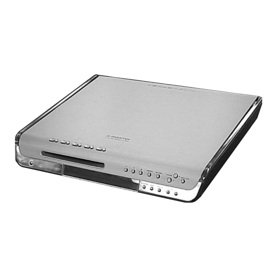
HCD-FC7 is the amplifier, DVD/SACD and tuner
section in DAV-FC7.
AUDIO POWER SPECIFICATIONS POWER
OUTPUT AND TOTAL HARMONIC
TE
L 13942296513
DISTORTION:
With 4 ohm loads, both channels driven, from 20 –
20,000 Hz; rated 75 watts per channel minimum RMS
power, with no more than 0.7 % total harmonic
distortion. (from 250 milli watts to rated output)
Amplifier section
Stereo mode
Surround mode
* Depending on the sound field settings and the source,
there may be no sound output.
Inputs
Outputs
www
.
Sony Corporation
9-961-034-01
2003H1678-1
Home Audio Company
© 2003.08
Published by Sony Engineering Corporation
http://www.xiaoyu163.com
Super Audio CD/DVD system
Laser
Signal format system
Frequency response (at 2 CH STEREO mode)
100 W + 100 W (4 ohms
at 1 kHz, THD 10 %)
Front:
100
W +
100
W
centre*:
100
W
Harmonic distortion
100
Surround*:
W +
100
W (4 ohms at 1 kHz,
Tuner section
THD 10 %)
System
100
Subwoofer*:
W
(4 ohms at 100 Hz, THD
FM tuner section
10 %)
Tuning range
North American models: 87.5 – 108.0 MHz
Other models:
VIDEO 1:
Antenna
Sensitivity: 150 mV
Antenna terminals
Impedance: 50 kilohms
Intermediate frequency
VIDEO 2:
AM tuner section
Sensitivity: 300 mV
Tuning range
Impedance: 50 kilohms
North American models: 531 – 1,710 kHz (with the
VIDEO 1 (AUDIO
OUT):
Voltage: 1 V
Impedance: 1 kilohm
Other models:
PHONES:
Accepts stereo
headphones only.
x
ao
u163
y
Antenna
Intermediate frequency
i
http://www.xiaoyu163.com
HCD-FC7
2 9
8
Model Name Using Similar Mechanism
Mechanism Type
Base Unit Name
Optical Pick-up Name
SPECIFICATIONS
Q Q
S
emiconductor laser
3
6 7
1 3
1 5
(Super Audio CD/DVD:
λ
= 650 nm)
λ
(CD:
= 780 nm)
Emi
ssion duration:
continuous
NTSC or NTSC/PAL
DVD (PCM): 2 Hz to
22 kHz (±1.0 dB)
CD: 2 Hz to 20 kHz
(±1.0 dB)
Less than 0.03 %
PLL quartz-locked digital
synthesizer system
(100 kHz step)
87.5 – 108.0 MHz
(50 kHz step)
FM wire antenna
75 ohms, unbalanced
10.7 MHz
interval set at 9 kHz)
530 – 1,710 kHz (with the
interval set at 10 kHz)
531 – 1,602 kHz (with the
interval set at 9 kHz)
530 – 1,710 kHz (with the
co
interval set at 10 kHz)
AM loop antenna
450 kHz
.
9 4
2 8
US Model
Canadian Model
E Model
Australian Model
HCD-C770
CDM69-DVBU16
DVBU16
TDP022W
Video section
Inputs
Video: 1 Vp-p 75 ohms
0 5
8
2 9
9 4
2 8
Outputs
Video: 1 Vp-p 75 ohms
S video:
Y: 1 Vp-p 75 ohms
C: 0.286 Vp-p 75 ohms
COMPONENT:
Y: 1 Vp-p 75 ohms
P
/C
, P
B
B
R
75 ohms
General
Power requirements
North American models: 120 V AC, 60 Hz
Australian and Asian models:
220 – 240 V AC, 50/60 Hz
Power consumption
North American models: 135 W
Australian and Asian models:
135 W
×
Dimensions (approx.)
380
70
×
( 15 2
/
7
8
(w/h/d) incl. projecting
parts
Mass (approx.)
4.8 kg (10 lb 10 oz)
Operating temperature
5°C to 35°C (41°F to 95°F)
Operating humidity
5 % to 90 %
Design and specification are subject to change without
notice.
m
SACD/DVD RECEIVER
9 9
9 9
/C
: 0.7 Vp-p
R
×
345 mm
×
13
/
inches)
5
8
Advertisement
Table of Contents

Related Manuals for Sony hcd-fc7


Summary of Contents for Sony hcd-fc7
-
Page 1: Service Manual
3 7 63 1515 0 SERVICE MANUAL US Model Canadian Model Ver 1.0 2003. 08 E Model Australian Model HCD-FC7 is the amplifier, DVD/SACD and tuner section in DAV-FC7. Model Name Using Similar Mechanism HCD-C770 Mechanism Type CDM69-DVBU16 Base Unit Name... -
Page 2: Leakage Test
CRITIQUES POUR LA SÉCURITÉ DE FONCTIONNEMENT. NE COMPONENTS WITH SONY PARTS WHOSE PART NUMBERS REMPLACER CES COMPOSANTS QUE PAR DES PIÈSES SONY APPEAR AS SHOWN IN THIS MANUAL OR IN SUPPLEMENTS DONT LES NUMÉROS SONT DONNÉS DANS CE MANUEL OU PUBLISHED BY SONY. -
Page 3: Table Of Contents
HCD-FC7 3 7 63 1515 0 TABLE OF CONTENTS 1. SERVICING NOTE 7-12. SCHEMATIC DIAGRAM ·························································· 4 – DVD SECTION (4/10) – ·········································· 50 7-13. SCHEMATIC DIAGRAM 2. GENERAL ·········································································· 7 – DVD SECTION (5/10) – ·········································· 51 7-14. SCHEMATIC DIAGRAM 3. -
Page 4: Servicing Note
HCD-FC7 SECTION 1 SERVICING NOTE 3 7 63 1515 0 MODEL IDENTIFICATION NOTES ON HANDLING THE OPTICAL PICK-UP BLOCK — BACK PANEL — OR BASE UNIT The laser diode in the optical pick-up block may suffer electrostatic break-down because of the potential difference generated by the charged electrostatic load, etc. - Page 5 HCD-FC7 3 7 63 1515 0 • Service position of POWER board POWER board power cord Power cord is directly connected without going via LF board . L 13942296513 • Service position of DVD board J-2501-242-A (1mm/11P/L300) AMP board...
- Page 6 HCD-FC7 3 7 63 1515 0 • Service position of AMP board AMP board AMP board cannot be moved unless it removes side panel and back panel . L 13942296513 u163 http://www.xiaoyu163.com...
-
Page 7: General
HCD-FC7 SECTION 2 GENERAL 3 7 63 1515 0 This section is extracted from instruction manual. Front Panel A Disc slot (24) I PHONES jack (on the side of the system) (24) B DISC 1-5 A (eject)/indicators (24) J SOUND FIELD –/+ (47, 48, 49) - Page 8 HCD-FC7 3 7 63 1515 0 Rear Panel SCAN SELECT FRONT R CENTER FRONT L MONITOR OUT S VIDEO VIDEO 1 VIDEO 2 VIDEO AUDIO OUT VIDEO OUT AUDIO IN VIDEO IN SELECTABLE SURR R WOOFER SURR L INTERLACE...
- Page 9 HCD-FC7 3 7 63 1515 0 G PLAY MODE (33, 34, 35) Remote H CLEAR (34, 35, 36, 38) I TV (59) J AUDIO (45) K ANGLE (51) L SUBTITLE (52) M ./>, PREV/NEXT, PRESET –/+ (26, 28, 60, 61)
-
Page 10: Disassembly
HCD-FC7 SECTION 3 DISASSEMBLY 3 7 63 1515 0 • The equipment can be removed using the following procedure. FRONT PANEL SECTION, SIDE PANEL (L)/(R) SECTION DDCON BOARD, LED BOARD, POWER BOARD FL BOARD KEY BOARD AMP BOARD DVD BOARD,... -
Page 11: Side Panel (L)/(R) Section
HCD-FC7 3 7 63 1515 0 Note: Follow the disassembly procedure in the numerical order given. 3-1. FRONT PANEL SECTION, SIDE PANEL (L)/(R) SECTION front panel section 4 wire (flat type)(CN005) 6 two screws 2 four screws (+BVTP 3 × 8) -
Page 12: Ddcon Board, Led Board, Fl Board
HCD-FC7 3 7 63 1515 0 3-2. DDCON BOARD, LED BOARD, FL BOARD qf panel top (R) qs band button qa panel top (L) 8 wire (flat type) 9 FL board qd three screws (+BVTP 3 × 8) qg front (ml) panel 0 three screws (+BVTP 3 ×... -
Page 13: Power Board
HCD-FC7 3 7 63 1515 0 3-4. POWER BOARD 1 screw 7 connector (CN903) (+BVTP 3 × 8) 2 power sheet 4 two screws (+BVTP 3 × 8) 6 connector (CN904) 3 connector (CN902) 5 screw (+BVTP 3 × 8) -
Page 14: Dvd Board, Dc Fan
HCD-FC7 3 7 63 1515 0 3-6. DVD BOARD, DC FAN 3 two screws 5 two screws (+BVTP 3 × 8) (+BVTP 3 × 8) 8 wire (flat type)(CN001) 4 sheet 0 connector (CN008) 6 power bracket 7 wire (flat type)(CN002) -
Page 15: Cd Mechanism Deck (Cdm69-Dvbu16)
HCD-FC7 3 7 63 1515 0 3-7. CD MECHANISM DECK (CDM69-DVBU16) 1 two screws (BVTP 3 × 8) 2 two screws (BVTP 3 × 8) 6 wire (flat type) (CN002) 7 CD mechanism deck (CDM69-DVBU16) 5 wire (flat type) -
Page 16: Lf Board
HCD-FC7 3 7 63 1515 0 3-8. SELECTOR BOARD, VIDEO BOARD, LF BOARD qs two screws (+BVTP 3 × 8) qd LF board 5 two screws 9 two screws (+BTP 3 × 6) (+BVTP 3 × 8) 1 screw 6 md cover (+BVTP 3 ×... -
Page 17: Base Unit (Dvbu16)
HCD-FC7 3 7 63 1515 0 3-10. BASE UNIT (DVBU16) 3 boss 1 screw (PTPWHM2.6) 5 boss 4 boss 6 base unit (DVBU16) L 13942296513 3-11. PICK-UP UNIT (TDP022W) 1 step screw (M) 2 step screw (M) 7 insulator... -
Page 18: Sw Board, Bracket (Top) Assy
HCD-FC7 3 7 63 1515 0 3-12. SW BOARD, BRACKET (TOP) ASSY 4 SW board (3) 3 SW board (2) 5 SW board (4) 1 four screws 6 six screws (BTP2.6 × 6) (BVTP2.6 × 8) 2 SW board (1) -
Page 19: Motor (Stocker) Assy (Stocker)(M761)
HCD-FC7 3 7 63 1515 0 3-14. MOTOR (STOCKER) ASSY (STOCKER)(M761) 3 two screws (BVTP2.6 × 8) 2 Remove two solders 6 STOCKER MOTOR board 5 connector (CN761) 7 motor (stocker) assy (stocker) (M761) 1 belt (stocker) L 13942296513 3-15. -
Page 20: Motor (Stocker) Assy (Mode)(M771)
HCD-FC7 3 7 63 1515 0 3-16. MOTOR (STOCKER) ASSY (MODE)(M771) 3 two screws 1 Remove five solders (BVTP2.6 × 8) of rotary encoder. 4 MODE MOTOR board 6 motor (stocker) assy MODE MOTOR (mode) (M771) board 2 Remove two solders... -
Page 21: Timing Belt (Front/Rear)
HCD-FC7 3 7 63 1515 0 3-18. TIMING BELT (FRONT/REAR) 3 slider (mode cam) assy 7 two gears (center) When install three timing belts, its pass under each claws. 8 timing belt (rear) timing belt (rear) 5 two gears... -
Page 22: Sensor Board
HCD-FC7 3 7 63 1515 0 3-20. SENSOR BOARD qj claw qk harness 9 cam (eject lock) 8 screw (PTPWH2.6 × 8) qs gear qg two claws (eject lock) qa cam w; SENSOR board qh rotary encoder (BU U/D) -
Page 23: Assembly
HCD-FC7 SECTION 4 ASSEMBLY 3 7 63 1515 0 • This set can be assembled in the order shown below. 4-1. HOW TO INSTALL THE CAM (EJECT LOCK) 1 Rotate the cam (BU U/D) fully in the direction of arrow. -
Page 24: How To Install The Gear (Mode 2)
HCD-FC7 3 7 63 1515 0 4-3. HOW TO INSTALL THE GEAR (MODE 2) 1 Align the mark on the rotary encoder (S771) with the projection of the assy. 2 Check that the cam (BU U/D) can not be rotated in the direction of arrow. -
Page 25: How To Install The Rotary Encoder (S702), Gear (Stocker Communication)
HCD-FC7 3 7 63 1515 0 4-5. HOW TO INSTALL THE ROTARY ENCODER (S702), GEAR (STOCKER COMMUNICATION) 4 gear 5 screw (PTPWH2.6 × 8) (stocker communication) 3 screw 7 two screws (PWH2 × 6) (PTPWH2.6 × 8) 1 rotary encoder... -
Page 26: Test Mode
HCD-FC7 SECTION 5 TEST MODE 3 7 63 1515 0 [Version Display Mode] [OSD Test Mode] * The software version is displayed. Procedure: Press the ?/1 button on the main unit or the ?/1 button on Procedure: Press three buttons of [FUNCTION], x and A (DISC 1) the remote commander to turn the set on. - Page 27 HCD-FC7 3 7 63 1515 0 [GENERAL DESCRIPTION] 0-1. All (All items continuous check) This menu checks all diagnostic items continuously. Normally, all The Test Mode allows you to make diagnosis and adjustment easily items are checked successively one after another automatically using the remote commander and monitor TV.
- Page 28 HCD-FC7 3 7 63 1515 0 0-2-4. Model Type 1-1. DVD-SL (single layer) Press the 1 key on the remote commander and insert a DVD single Model name is displayed. (DAV-FC7) layer disc following the message. Then the adjustment will be made 0-2-5.
- Page 29 HCD-FC7 3 7 63 1515 0 24. Auto track gain adjust DRIVE MANUAL OPERATION Search Check Note: This mode is used for design, and not used in service fundamen- 25. 32Tj forward tally. 26. 32Tj reverse On the Test Mode Menu screen, press the key on the remote 27.
- Page 30 HCD-FC7 3 7 63 1515 0 2-1. Disc Type 2-1-3. Disc Type CD It sets up so that it may judge as a disc type of specification of the disc with which the set was inserted. Disc Type : CD disc (normal speed, 12 cm)
- Page 31 HCD-FC7 3 7 63 1515 0 2-3. Track/Layer Jump 2-5. EEPROM Write Adjust Track/Layer Jump EEPROM Write Adjust FWD R.Lj L0>L1 REV L.Lj L1>L0 1. Focus Offset 3.500Tj Fine FWD U.Fj L0>L1 2. Focus Gain 4.500Tj Fine REV D.Fj L1>L0 3.
- Page 32 HCD-FC7 3 7 63 1515 0 2-7. Disc Check Memory MECHA AGING On the Test Mode Menu screen, selecting executes the aging of Disc Check Memory the mechanism deck. 1. SL Disc check ### Aging Test MENU ### 2. CD Disc check ** Pls use over 40min.
- Page 33 HCD-FC7 3 7 63 1515 0 • Code list of Emergency History • Error code (aa) 10: Communication to RF AMP (IC001) failed. FF : Complete the initializing. (normal operation) 11: Each servo for focus, tracking, and spindle is unlocked.
-
Page 34: Electrical Adjustment
HCD-FC7 SECTION 6 ELECTRICAL ADJUSTMENT 3 7 63 1515 0 AUTO SERVO ADJUSTMENT VERSION INFORMATION After parts related to the servo circuit (RF amplifier (IC001), DSP On the Test Mode Menu screen, selecting displays the ROM (IC401), motor driver (IC501), EEPROM (IC302) so on) are version and region code. -
Page 35: Diagrams
HCD-FC7 SECTION 7 DIAGRAMS 3 7 6 3 1 5 1 5 0 7-1. CIRCUIT BOARDS LOCATION THIS NOTE IS COMMON FOR PRINTED WIRING BOARDS AND SCHEMATIC DIAGRAMS. (In addition to this, the necessary note is printed in each block.) For schematic diagrams. -
Page 36: Block Diagrams - Rf/Servo Section
HCD-FC7 7-2. BLOCK DIAGRAMS – RF/SERVO SECTION – 3 7 6 3 1 5 1 5 0 • SIGNAL PATH WARFI AUDIO(DSP) : AUDIO SECTION : CD CDDOUT AUDIO(DSP) : DVD : VIDEO SECTION : SACD 117 RFIN SD0 – SD7... -
Page 37: Audio Section
HCD-FC7 – AUDIO SECTION – 3 7 6 3 1 5 1 5 0 IC402 (2/2) REFERENCE VOLTAGE GENERATOR 127 WAVRB WARFI D1 – D4, SCK, RF/SERVO 126 WARFI 39 DSIFL DSAL BCKO, LRCKO AUDIO OUT SECTION SDO4 SECTION... -
Page 38: Audio Out Section
HCD-FC7 – AUDIO OUT SECTION – 3 7 6 3 1 5 1 5 0 IC608 IC301 D/A CONVERTER STREAM PROCESSOR • SIGNAL PATH 3 SDTI AOUTL+ J900 : AUDIO HPOUTL1 J205 (2/4) AOUTL– PHONES IC610 HPOUTL2 VIDEO 1... -
Page 39: Video Section
HCD-FC7 – VIDEO SECTION – 3 7 6 3 1 5 1 5 0 J205 (3/4) • SIGNAL PATH VIDEO 1 : VIDEO VIDEO IN IC207 VIDEO INPUT J206 (2/3) SELECTOR IC209 VIDEO 2 : CHROMA VIDEO SELECTOR VIDEO IN... -
Page 40: Power Section
HCD-FC7 – POWER SECTION – 3 7 6 3 1 5 1 5 0 T801 DC-DC CONVERTER IC902 FL58 IC721 CHANGER CONTROLLER STOCKER MOTOR DRIVE (MOTOR, SWITCH) TO FLUORESCENT INDICATOR TUBE D806 – 809 M761 OUT1 RECT (STOCKER) OUT2... -
Page 41: Printed Wiring Board - Rf Section
HCD-FC7 7-3. PRINTED WIRING BOARD – RF SECTION – • See page 35 for Circuit Boards Location. • : Uses unleaded solder. 3 7 6 3 1 5 1 5 0 RF BOARD RF BOARD (SIDE A) (SIDE B) -
Page 42: Schematic Diagram - Rf Section
HCD-FC7 7-4. SCHEMATIC DIAGRAM – RF SECTION – • See page 70 for Waveforms. • See page 80 for IC Block Diagrams. 3 7 6 3 1 5 1 5 0 RFMON C006 C028 C027 R026 C013 C031 1000p... -
Page 43: Changer Section
HCD-FC7 7-5. PRINTED WIRING BOARD – CHANGER SECTION – • See page 35 for Circuit Boards Location. • : Uses unleaded solder. 3 7 6 3 1 5 1 5 0 • Semiconductor RELAY BOARD STOCKER MOTOR BOARD Location SW (4) BOARD Ref. -
Page 44: Changer Section
HCD-FC7 7-6. SCHEMATIC DIAGRAM – CHANGER SECTION – • See page 79 for IC Block Diagrams. 3 7 6 3 1 5 1 5 0 CNP751 CN702 R731 DIODE DIODE IC751 D SENSE D SENSE R733 CN701 R734 IC751... -
Page 45: Dvd Section (Side A)
HCD-FC7 7-7. PRINTED WIRING BOARD – DVD SECTION (SIDE A) – • See page 35 for Circuit Boards Location. • : Uses unleaded solder. 3 7 6 3 1 5 1 5 0 RELAY BOARD • Semiconductor CN701 Location (Page 43) Ref. -
Page 46: Dvd Section (Side B)
HCD-FC7 7-8. PRINTED WIRING BOARD – DVD SECTION (SIDE B) – • See page 35 for Circuit Boards Location. • : Uses unleaded solder. 3 7 6 3 1 5 1 5 0 • Semiconductor Location Ref. No. Location... -
Page 47: Schematic Diagram
HCD-FC7 7-9. SCHEMATIC DIAGRAM – DVD SECTION (1/10) – • See page 73 for IC Block Diagrams. 3 7 6 3 1 5 1 5 0 FL401 C401 C402 CN401 R411 TO RF AMP R412 JL544 C404 R413 JL537... -
Page 48: Dvd Section (2/10)
HCD-FC7 7-10. SCHEMATIC DIAGRAM – DVD SECTION (2/10) – 3 7 6 3 1 5 1 5 0 C526 R581 C527 R582 R583 R580 C519 0.01 R579 8.2k IC501 FAN8035 R534 R535 R533 C514 0.01 1 3 9 4 2 2 9 6 5 1 3... -
Page 49: Schematic Diagram
HCD-FC7 7-11. SCHEMATIC DIAGRAM – DVD SECTION (3/10) – • See page 70 for Waveforms. • See page 75 for IC Block Diagrams. 3 7 6 3 1 5 1 5 0 R729 C715 TP701 8.2k 0.0015 IC703(2/2) C703... -
Page 50: Schematic Diagram
HCD-FC7 7-12. SCHEMATIC DIAGRAM – DVD SECTION (4/10) – • See page 76 for IC Block Diagrams. 3 7 6 3 1 5 1 5 0 C870 33000p R803 IC702 C795 TA48M025F(TE16L) IC808 6.3V MSM56V16160F-8TK C796 C797 FL810 FL811... -
Page 51: Schematic Diagram
HCD-FC7 7-13. SCHEMATIC DIAGRAM – DVD SECTION (5/10) – • See page 70 for Waveforms. • See page 75 for IC Block Diagrams. 3 7 6 3 1 5 1 5 0 C303 0.01 FL301 Q301 DTC114EKA -T146 C301 C302 0.01... -
Page 52: Schematic Diagram
HCD-FC7 7-14. SCHEMATIC DIAGRAM – DVD SECTION (6/10) – • See page 70 for Waveforms. • See page 72 for IC Block Diagrams. 3 7 6 3 1 5 1 5 0 CN003 TP023 R013 TP024 R015 TP025 FB004... -
Page 53: Schematic Diagram
HCD-FC7 7-15. SCHEMATIC DIAGRAM – DVD SECTION (7/10) – • See page 72 for IC Block Diagrams. 3 7 6 3 1 5 1 5 0 IC202 HY57V283220T-6 C217 0.01 C219 0.01 C226 0.01 C234 0.01 C238 0.01 C274 0.01... -
Page 54: Schematic Diagram
HCD-FC7 7-16. SCHEMATIC DIAGRAM – DVD SECTION (8/10) – • See page 70 for Waveforms. • See page 73, 74, 75 for IC Block Diagrams. 3 7 6 3 1 5 1 5 0 IC600 IC601 NJM78M05DL1A -TE1 R600... -
Page 55: Schematic Diagram
HCD-FC7 7-17. SCHEMATIC DIAGRAM – DVD SECTION (9/10) – • See page 70 for Waveforms. • See page 76 for IC Block Diagrams. 3 7 6 3 1 5 1 5 0 CN900 FB901 FB902 Q908 DTC124EKA R992 C900... -
Page 56: Dvd Section (10/10)
HCD-FC7 7-18. SCHEMATIC DIAGRAM – DVD SECTION (10/10) – 3 7 6 3 1 5 1 5 0 IC006 C018 C020 C019 IC004 IC005 C015 C014 C016 C017 IC003 1 3 9 4 2 2 9 6 5 1 3... -
Page 57: Amp Section (Side A)
HCD-FC7 7-19. PRINTED WIRING BOARD – AMP SECTION (SIDE A) – • See page 35 for Circuit Boards Location. • : Uses unleaded solder. 3 7 6 3 1 5 1 5 0 • Semiconductor Location Ref. No. Location... -
Page 58: Amp Section (Side B)
HCD-FC7 7-20. PRINTED WIRING BOARD – AMP SECTION (SIDE B) – • See page 35 for Circuit Boards Location. • : Uses unleaded solder. 3 7 6 3 1 5 1 5 0 SPEAKER FRONT R CEINTER FRONT L... -
Page 59: Schematic Diagram
HCD-FC7 7-21. SCHEMATIC DIAGRAM – AMP SECTION (1/2) – • See page 70 for Waveforms. • See page 71 for IC Block Diagrams. 3 7 6 3 1 5 1 5 0 CN304 CN303 CN301 CN302 CNP301 L901 C991 0.047... -
Page 60: Amp Section (2/2)
HCD-FC7 7-22. SCHEMATIC DIAGRAM – AMP SECTION (2/2) – 3 7 6 3 1 5 1 5 0 R384 IC106 CXD9750L IC105 CXD9750L IC104 CXD9750L IC103 CXD9750L C104 C103 C102 IC102 CXD9750L IC101 CXD9750L C106 C105 C101 0.01 0.01 0.01... -
Page 61: Audio Section
HCD-FC7 7-23. PRINTED WIRING BOARD – AUDIO SECTION – • See page 35 for Circuit Boards Location. • : Uses unleaded solder. 3 7 6 3 1 5 1 5 0 • Semiconductor Location Ref. No. Location D202 D203... -
Page 62: Schematic Diagram
HCD-FC7 7-24. SCHEMATIC DIAGRAM – AUDIO SECTION – • See page 71 for IC Block Diagrams. 3 7 6 3 1 5 1 5 0 CN201 R212 C213 0.0033 D203 D202 MA111-TX MA111-TX C214 0.0033 CN205 CNP205 S826 L205... -
Page 63: Video Section
HCD-FC7 7-25. PRINTED WIRING BOARD – VIDEO SECTION – • See page 35 for Circuit Boards Location. • : Uses unleaded solder. 3 7 6 3 1 5 1 5 0 • Semiconductor Location Ref. No. Location IC204 IC206... -
Page 64: Schematic Diagram
HCD-FC7 7-26. SCHEMATIC DIAGRAM – VIDEO SECTION – • See page 70 for Waveforms. • See page 81 for IC Block Diagrams. 3 7 6 3 1 5 1 5 0 C218 IC206 1000 MM1510 XNRE 6.3V L202 C252... -
Page 65: Ddcom Section
HCD-FC7 7-27. PRINTED WIRING BOARD – DDCOM SECTION – • See page 35 for Circuit Boards Location. • : Uses unleaded solder. 3 7 6 3 1 5 1 5 0 IC800 • Semiconductor Location Ref. No. Location D806... -
Page 66: Control Section
HCD-FC7 7-28. PRINTED WIRING BOARD – CONTROL SECTION – • See page 35 for Circuit Boards Location. • : Uses unleaded solder. 3 7 6 3 1 5 1 5 0 IC802 IC801 FUNCTION (FLUORESCENT INDICATOR TUBE) 1 3 9 4 2 2 9 6 5 1 3... -
Page 67: Schematic Diagram
HCD-FC7 7-29. SCHEMATIC DIAGRAM – DDCOM/CONTROL SECTION – • See page 70 for Waveforms. • See page 71, 77 for IC Block Diagrams. 3 7 6 3 1 5 1 5 0 D805 D804 D803 D802 D801 SML-020MDT SML-020MDT... -
Page 68: Power Section
HCD-FC7 7-30. PRINTED WIRING BOARD – POWER SECTION – • See page 35 for Circuit Boards Location. • : Uses unleaded solder. 3 7 6 3 1 5 1 5 0 BOARD BOARD • Semiconductor CN301 CN008 Location (Page 58) -
Page 69: Schematic Diagram
HCD-FC7 7-31. SCHEMATIC DIAGRAM – POWER SECTION – • See page 70 for Waveforms. • See page 78, 79 for IC Block Diagrams. 3 7 6 3 1 5 1 5 0 LF901 CN900 CN901 C903 CN904 D911 FML-22S... - Page 70 HCD-FC7 3 7 6 3 1 5 1 5 0 • Waveforms — RF Board — — DDCOM Board — — AMP Board — IC001 1 (DVDRFP) IC001 el (TE) IC001 r; (FE) IC001 tj (RFAC) Q803 collector IC304 4 IC301, 302, 303 2 (OUTL1) 4.2 Vp-p...
-
Page 71: Ic Block Diagrams
HCD-FC7 3 7 63 1515 0 7-32. IC BLOCK DIAGRAMS – AUDIO BOARD – – AMP BOARD – IC202 MC14052 BDR2 IC305 NJM4580E (TE2) A OUT A –IN B OUT A +IN B –IN B +IN V– – DDCON BOARD –... - Page 72 HCD-FC7 3 7 63 1515 0 – DVD BOARD – IC203 BR9040F-WE2 IC215 SN74ALVCH16841DGGR 56 1LE COMMAND 4096bit REGISTER EEPROM ARRAY WRITE DISABLE POWER ADDRESS HIGH VOLTAGE SUPPLY DECODER GENERATOR VOLTAGE DETECTOR LATCH COMMAND DECODE ADDRESS DATA CONTROL CLOCK...
- Page 73 HCD-FC7 3 7 63 1515 0 IC401 CXD3068Q 60 59 58 55 54 53 52 50 49 48 46 45 44 43 42 41 DVDD2 ASYE TES1 DOUT TEST DVSS1 LRCK PCMD FRDR BCLK FFDR EMPH TRDR TFDR XTSL...
- Page 74 HCD-FC7 3 7 63 1515 0 IC604 IS61LV6416-10TLT ROW/COLUMN DECODER OUTPUT ENABLE BUFFER 64K x 16 BYTE ENABLE MEMORY CHIP ENABLE BUFFER ARRAY BUFFER I/O 15 I/O 0 I/O 14 I/O 1 I/O 13 I/O 2 I/O 12 I/O 3...
- Page 75 HCD-FC7 3 7 63 1515 0 IC608 AK4382AVT-E2 DZFL CLOCK DE–EMPHASIS MCLK DZFR DIVIDER CONTROL ∆∑ AOUTL+ INTERPOLATOR MODULATOR BICK AOUTL– AUDIO SDTI DATA INTERFACE ∆∑ LRCK AOUTR+ INTERPOLATOR MODULATOR AOUTR– µP CCLK INTERFACE CDTI IC706 MSM51V18165F-60TSKR1 40 – 36...
- Page 76 HCD-FC7 3 7 63 1515 0 IC808 MSM56V16160F-8TK7R1 35 34 TIMING REGISTER PROGRAMING OUTPUT REGISTER BUFFERS LATENCY INTERNAL INTERNAL COLUMN & COLUMN READ ADDRESS ADDRESS BURST ADDRESS ADDRESS DATA BUFFERS BUFFERS CONTROLLER COUNTOR COUNTOR REGISTER CONTROLLER INPUT DATA SENSE...
- Page 77 HCD-FC7 3 7 63 1515 0 – FL BOARD – IC802 MSM9202-05GS-KDR1 Timing Timing Generator 2 Generator 1 64 VDD Duty Control Digit 63 DAT 8bit Control Shift 62 CLK Register 61 CS Port Control Driver Circuit 60 RST...
- Page 78 HCD-FC7 3 7 63 1515 0 – POWER BOARD – IC901 STR-F6238S (US, Canadian models) IC901 STR-F6267D (Australian, Singapore models) DRIVE REGULATOR OVER CURRENT PROTECTOR OVER INH1 VOLTAGE START PROTECTOR LATCH THERMAL SHUT DOWN FEED BACK INH2 OVER LOAD...
- Page 79 HCD-FC7 3 7 63 1515 0 IC906 SI-8033JF IC908 SI-8120JF OVER OVER CURRENT CURRENT REGULATOR REGULATOR PROTECTOR PROTECTOR LATCH LATCH RESET RESET & & ON/OFF ON/OFF DRIVER DRIVER SOFT SOFT COMPARATOR COMPARATOR START START OVER HEAT OVER HEAT –...
- Page 80 HCD-FC7 3 7 63 1515 0 – RF BOARD – IC001 CXD1881AR 64 63 62 61 60 59 55 54 53 52 FAST ATTACK INPUT OUTPUT HOLD FULL WAVE AGC CHARGE INHIBIT RECTIFER PUMP PROGRAMMABLE FROM S-PORT EQUALIZER INPUT...
- Page 81 HCD-FC7 3 7 63 1515 0 – VIDEO BOARD – IC206 MM1510XNRE IC207 NJM2235V (TE2) 6 SW OUT2 IN 1 BUFFER OUT1 DRIVER 5 GND SW 1 IN 2 CLAMP BIAS BIAS SW 2 VIN 3 IC208 MM1568AJBE VCC1...
-
Page 82: Ic Pin Function Description
HCD-FC7 3 7 63 1515 0 7-33. IC PIN FUNCTION DESCRIPTION • DVD BOARD IC206 ZIVA5X-C1F (DVD SYSTEM PROCESSOR) Pin No. Pin Name Description VDDP — Power supply terminal (+3.3V) (I/O signal) Address bus HD15 Data bus (address signal multiplexed) - Page 83 HCD-FC7 3 7 63 1515 0 Pin No. Pin Name Description MRAS SDRAM row address strobe signal output MCAS SDRAM column address strobe signal output SDRAM write enable signal output (“H” : read, “L” : write) GND25 — Ground terminal (SDRAM I/O signal) VDD25 —...
- Page 84 HCD-FC7 3 7 63 1515 0 Pin No. Pin Name Description MD30 SDRAM data MD31 SDRAM data GND25 — Ground terminal (SDRAM I/O signal) VDD25 — Power supply terminal (+3.3V) (SDRAM I/O signal) VCLK System clock (not used) I2C_CTRL —...
- Page 85 HCD-FC7 3 7 63 1515 0 Pin No. Pin Name Description GPIO4 (2) — Not used (pull-up) VDDP — Power supply terminal (+3.3V) (I/O signal) GNDP — Ground terminal (I/O signal) GPIO4 (3) — Not used (pull-down) GPIO4 (4) —...
- Page 86 HCD-FC7 3 7 63 1515 0 Pin No. Pin Name Description TCK signal input RESET ZIVA reset input BUS CLK Not used — Ground terminal (inside core) — Power supply terminal (+1.8V) (inside core) Address bus 3 Address bus 2 GNDP —...
- Page 87 HCD-FC7 3 7 63 1515 0 • DVD BOARD IC301 CXP973064-228R (MACHANISH CONTROLLER) Pin No. Pin Name Description EEP SO Not used SDEN Serial data enable signal output to DVD/CD RF amplifier DOCTRL/ Digital out on/off control signal output to the digital signal processor ISBTEST “L”: digital out off, “H”: digital out on...
- Page 88 HCD-FC7 3 7 63 1515 0 Pin No. Pin Name Description SQSO Subcode Q data input from the digital signal processor MUTE DSD Muting on/off control signal output to the DSD decoder “H”: muting on SQCK Subcode Q data reading clock signal output to the digital signal processor —...
- Page 89 HCD-FC7 3 7 63 1515 0 • DVD BOARD IC401 CXD3068Q (DIGITAL SIGNAL PROCESSOR, DIGITAL SERVO PROCESSOR) Pin No. Pin Name Description DVDD0 — Power supply terminal (+3.3V) (digital system) XRST Reset signal input from the mechanism controller “L”: reset MUTE Muting on/off control signal input from the mechanism controller “H”: muting on...
- Page 90 HCD-FC7 3 7 63 1515 0 Pin No. Pin Name Description AVDD0 — Power supply terminal (+3.3V) (analog system) ASYO EFM full-swing output terminal ASYI Asymmetry comparator voltage input terminal RFAC EFM signal input from the DVD/CD RF amplifier AVSS1 —...
- Page 91 HCD-FC7 3 7 63 1515 0 • DVD BOARD IC607 CXD9617R (AUDIO DIGITAL SIGNAL PROCESSOR) Pin No. Pin Name Description — Ground terminal XRST Reset signal input from the system controller “L”: reset EXTIN Master clock signal input terminal Not used...
- Page 92 HCD-FC7 3 7 63 1515 0 Pin No. Pin Name Description VDDE — Power supply terminal (+3.3V) WMD1 S-RAM wait mode setting terminal Fixed at “H” in this set — Ground terminal WMD0 S-RAM wait mode setting terminal Fixed at “H ” in this set...
- Page 93 HCD-FC7 3 7 63 1515 0 Pin No. Pin Name Description SDI3 Rear L-ch and R-ch audio serial data input from the digital audio processor SDI4 Audio serial data input terminal Not used Synchronous/asychronous selection signal input terminal SYNC “L”: Synchronous, “H”: asynchronous (fixed at “H”...
- Page 94 HCD-FC7 3 7 63 1515 0 • DVD BOARD IC701 TMC57929PGF-RDP (DVD DECODER) Pin No. Pin Name Description 1, 2 D5, D6 Two-way data bus with the mechanism controller — Ground terminal (digital system) Two-way data bus with the mechanism controller Address signal input from the mechanism controller —...
- Page 95 HCD-FC7 3 7 63 1515 0 Pin No. Pin Name Description DVD mode: Serial data request signal input from the DVD system processor XHAC SACD mode: Serial data request signal input from the DSD decoder HINT Not used XS16...
- Page 96 HCD-FC7 3 7 63 1515 0 Pin No. Pin Name Description RFDCC Input terminal for adjusting DC cut high-pass filter for RF signal Not used RFIN RF signal input from the DVD/CD RF amplifier 118, 119 VCCA5, VCCA4 —...
- Page 97 HCD-FC7 3 7 63 1515 0 Pin No. Pin Name Description XTAL 33.8688 MHz clock signal input terminal — Ground terminal (digital system) XTL2 System clock output terminal (33.8688 MHz) XTL1 System clock input terminal (33.8688 MHz) — Power supply terminal (+3.3V) (digital system)
- Page 98 HCD-FC7 3 7 63 1515 0 • DVD BOARD IC801 CXD2753R (DSD DECODER) Pin No. Pin Name Description VSCA0 — Ground terminal (for core) XMSLAT Serial data latch pulse signal input from the mechanism controller MSCK Serial data transfer clock signal input from the mechanism controller...
- Page 99 HCD-FC7 3 7 63 1515 0 Pin No. Pin Name Description PHREFI Bit clock signal (2.8224 MHz) input terminal for DSD data output Not used PHREFO Bit clock signal (2.8224 MHz) output to the digital audio processor Not used...
- Page 100 HCD-FC7 3 7 63 1515 0 Pin No. Pin Name Description WRFD Not used Operation clock signal input for PSP physical disc mark detection from the DVD decoder WAVDD0, 124, 125 — A/D power supply terminal (+2.5V) (for PSP physical disc mark detection)
- Page 101 HCD-FC7 3 7 63 1515 0 • DVD BOARD IC901 µPD703033BYGF-M43-3BA-A (SYSTEM CONTROLLER) Pin No. Pin Name Description DAMP-DATA Serial data output to the stream processors DAMP-CLK Serial data transfer clock signal output to the stream processors I2C-DATA Communication data bus with the DVD system processor and mechanism controller CQ-RST Reset signal output to the DVD system processor “L”: reset...
- Page 102 HCD-FC7 3 7 63 1515 0 Pin No. Pin Name Description DIP-RST Reset signal output to the power drivers “L”: reset DIP-OCP Protect signal input from the over load detection circuit ST-POWER System power on/off control signal output “H”: power on HP-MUTE Headphone muting on/off control signal output “L”: muting on...
- Page 103 HCD-FC7 3 7 63 1515 0 Description Pin No. Pin Name DVD-POWER DVD power on/off control signal output “H”: power on STOP System power stop signal input POWER-SW AC power detection signal input SIRCS Remote control signal input System wake up signal input by pressing any key on the front panel or remote commander or...
- Page 104 HCD-FC7 3 7 63 1515 0 • DVD BOARD IC902 PT8300R-TP (CHANGER CONTROLLER (MOTOR, SWITCH)) Pin No. Pin Name Description — Ground terminal RESET-B Reset signal input from the system controller “L”: reset Serial data transfer clock signal input from the system controller...
- Page 105 HCD-FC7 3 7 63 1515 0 • DVD BOARD IC906 PT8300R-TP (CHANGER CONTROLLER (ROTARY ENCODER)) Pin No. Pin Name Description — Ground terminal RESET-B Reset signal input from the system controller “L”: reset Serial data transfer clock signal input from the changer controller (motor, switch)
-
Page 106: Exploded Views
HCD-FC7 SECTION 8 EXPLODED VIEWS 3 7 63 1515 0 NOTE: • Abbreviation • -XX, -X mean standardized parts, so they may The components identified by mark 0 or AUS : Australian model have some difference from the original one. -
Page 107: Front Panel Section
HCD-FC7 3 7 63 1515 0 8-2. FRONT PANEL SECTION not supplied not supplied not supplied not supplied L 13942296513 not supplied FL801 not supplied Ref. No. Part No. Description Remark Ref. No. Part No. Description Remark 4-248-518-01 FRONT (AL) PANEL... -
Page 108: Chassis Section-1
HCD-FC7 3 7 63 1515 0 8-3. CHASSIS SECTION-1 not supplied not supplied F901 not supplied not supplied supplied not supplied not supplied not supplied not supplied not supplied L 13942296513 not supplied chassis section-2 Ref. No. Part No. -
Page 109: Chassis Section-2
HCD-FC7 3 7 63 1515 0 8-4. CHASSIS SECTION-2 mechanism deck section-1 (CDM69-DVBU16) not supplied not supplied not supplied not supplied L 13942296513 chassis section-3 not supplied Ref. No. Part No. Description Remark Ref. No. Part No. Description Remark... -
Page 110: Chassis Section-3
HCD-FC7 3 7 63 1515 0 8-5. CHASSIS SECTION-3 not supplied not supplied not supplied not supplied not supplied not supplied L 13942296513 not supplied not supplied not supplied Ref. No. Part No. Description Remark Ref. No. Part No. -
Page 111: Mechanism Deck Section-1
HCD-FC7 3 7 63 1515 0 8-6. MECHANISM DECK SECTION-1 (CDM69-DVBU16) S702 M761 L 13942296513 mechanism deck section-2 (CDM69-DVBU16) Ref. No. Part No. Description Remark Ref. No. Part No. Description Remark 1-685-006-11 STOCKER MOTOR BOARD 4-239-689-01 GEAR (STOCKER DECELERATION) 4-951-620-01 SCREW (2.6X8), +BVTP... -
Page 112: Mechanism Deck Section-2
HCD-FC7 3 7 63 1515 0 8-7. MECHANISM DECK SECTION-2 (CDM69-DVBU16) mechanism deck section-3 (CDM69-DVBU16) L 13942296513 mechanism deck section-4 (CDM69-DVBU16) base unit section (DVBU16) Ref. No. Part No. Description Remark Ref. No. Part No. Description Remark 1-685-008-11 SW (1) BOARD 4-951-620-01 SCREW (2.6X8), +BVTP... -
Page 113: Mechanism Deck Section-3
HCD-FC7 3 7 63 1515 0 8-8. MECHANISM DECK SECTION-3 (CDM69-DVBU16) not supplied supplied not supplied supplied supplied L 13942296513 not supplied not supplied Ref. No. Part No. Description Remark Ref. No. Part No. Description Remark 4-240-038-01 PULLEY (A), CHUCKING 4-239-651-01 ROLLER (STOCKER), RUBBER 4-992-069-01 SCREW (+PTPWH)(M2)(DIA. -
Page 114: Mechanism Deck Section-4
HCD-FC7 3 7 63 1515 0 8-9. MECHANISM DECK SECTION-4 (CDM69-DVBU16) supplied L 13942296513 not supplied M781 mechanism deck section-5 (CDM69-DVBU16) Ref. No. Part No. Description Remark Ref. No. Part No. Description Remark X-4954-626-1 LEVER (ROLLER) ASSY 4-240-981-01 SPRING (BASE SLIDER 5),TENSION... -
Page 115: Mechanism Deck Section-5
HCD-FC7 3 7 63 1515 0 8-10. MECHANISM DECK SECTION-5 (CDM69-DVBU16) L 13942296513 mechanism deck section-6 (CDM69-DVBU16) Ref. No. Part No. Description Remark Ref. No. Part No. Description Remark 4-240-020-01 GEAR (TIMING) 4-239-699-01 PULLEY 4-239-708-01 BELT (FRONT), TIMING 4-239-681-01 BELT (ROLLER) 4-239-697-01 GEAR (CENTER) 4-227-899-01 SCREW (DIA. -
Page 116: Mechanism Deck Section-6
HCD-FC7 3 7 63 1515 0 8-11. MECHANISM DECK SECTION-6 (CDM69-DVBU16) not supplied not supplied M771 L 13942296513 S771 Ref. No. Part No. Description Remark Ref. No. Part No. Description Remark 4-239-693-01 CAM (GEAR) 4-951-620-01 SCREW (2.6X8), +BVTP 1-685-004-11 SENSOR BOARD... -
Page 117: Base Unit Section (Dvbu16)
HCD-FC7 3 7 63 1515 0 8-12. BASE UNIT SECTION (DVBU16) L 13942296513 Ref. No. Part No. Description Remark Ref. No. Part No. Description Remark 4-981-923-01 SCREW (M), STEP 1-685-250-11 FLEXIBLE BOARD 3-053-847-31 INSULATOR 4-239-703-01 HOLDER (DBU1) 0 603 1-477-263-11 OPTICAL PICK-UP (TDP022W) 7-685-533-14 SCREW +BTP 2.6X6 TYPE2 N-S... - Page 118 HCD-FC7 SECTION 9 ELECTRICAL PARTS LIST 3 7 63 1515 0 Note: • CAPACITORS • Due to standardization, replacements in the parts When indicating parts by reference number, uF : µ F list may be different from the parts specified in the please include the board name.
- Page 119 HCD-FC7 3 7 63 1515 0 Ref. No. Part No. Description Remarks Ref. No. Part No. Description Remarks C243 1-104-665-11 ELECT 100uF 20.00% 10V C476 1-164-505-11 CERAMIC CHIP 2.2uF C244 1-104-665-11 ELECT 100uF 20.00% 10V C477 1-162-968-11 CERAMIC CHIP 0.0047uF 10%...
- Page 120 HCD-FC7 3 7 63 1515 0 Ref. No. Part No. Description Remarks Ref. No. Part No. Description Remarks FB302 1-469-760-21 INDUCTOR R106 1-216-845-11 METAL CHIP 100K 1/16W FB303 1-469-760-21 INDUCTOR R111 1-216-845-11 METAL CHIP 100K 1/16W FB304 1-469-760-21 INDUCTOR...
- Page 121 HCD-FC7 3 7 63 1515 0 AUDIO Ref. No. Part No. Description Remarks Ref. No. Part No. Description Remarks R343 1-216-837-11 METAL CHIP 1/16W C227 1-124-234-00 ELECT 22uF C228 1-164-156-11 CERAMIC CHIP 0.1uF R344 1-216-837-11 METAL CHIP 1/16W C230...
- Page 122 HCD-FC7 AUDIO 3 7 63 1515 0 DDCON Ref. No. Part No. Description Remarks Ref. No. Part No. Description Remarks < RESISTOR > A-4747-964-A DDCON BOARD, COMPLETE ********************** R208 1-216-813-11 METAL CHIP 1/16W R209 1-216-813-11 METAL CHIP 1/16W < CAPACITOR >...
- Page 123 HCD-FC7 3 7 63 1515 0 DDCON Ref. No. Part No. Description Remarks Ref. No. Part No. Description Remarks R810 1-216-809-11 METAL CHIP 1/16W C009 1-164-947-11 CERAMIC CHIP 0.01uF C010 1-107-820-11 CERAMIC CHIP 0.1uF R811 1-216-809-11 METAL CHIP 1/16W...
- Page 124 HCD-FC7 3 7 63 1515 0 Ref. No. Part No. Description Remarks Ref. No. Part No. Description Remarks C266 1-164-943-11 CERAMIC CHIP 0.01uF 10.00% 16V C436 1-125-777-11 CERAMIC CHIP 0.1uF 10.00% 10V C267 1-164-943-11 CERAMIC CHIP 0.01uF 10.00% 16V...
- Page 125 HCD-FC7 3 7 63 1515 0 Ref. No. Part No. Description Remarks Ref. No. Part No. Description Remarks C639 1-107-820-11 CERAMIC CHIP 0.1uF C727 1-117-370-11 CERAMIC CHIP 10uF C640 1-164-943-11 CERAMIC CHIP 0.01uF 10.00% 16V C728 1-125-777-11 CERAMIC CHIP 0.1uF...
- Page 126 HCD-FC7 3 7 63 1515 0 Ref. No. Part No. Description Remarks Ref. No. Part No. Description Remarks C842 1-164-943-11 CERAMIC CHIP 0.01uF 10.00% 16V D907 8-719-988-61 DIODE 1SS355TE-17 C843 1-164-943-11 CERAMIC CHIP 0.01uF 10.00% 16V C848 1-164-943-11 CERAMIC CHIP 0.01uF...
- Page 127 HCD-FC7 3 7 63 1515 0 Ref. No. Part No. Description Remarks Ref. No. Part No. Description Remarks IC202 6-704-069-01 IC HY57V283220T-6 Q901 8-729-230-63 TRANSISTOR 2SD1819A-QRS-TX * IC203 6-703-671-01 IC BR9040F-WE2 Q902 8-729-027-23 TRANSISTOR DTA114EKA-T146 IC205 6-803-225-01 IC MBM29DL324BE-90TN-FCV000...
- Page 128 HCD-FC7 3 7 63 1515 0 Ref. No. Part No. Description Remarks Ref. No. Part No. Description Remarks R052 1-218-990-11 SHORT CHIP R240 1-218-953-11 RES-CHIP 1/16W R241 1-218-953-11 RES-CHIP 1/16W R053 1-218-990-11 SHORT CHIP R242 1-218-965-11 RES-CHIP 1/16W R054...
- Page 129 HCD-FC7 3 7 63 1515 0 Ref. No. Part No. Description Remarks Ref. No. Part No. Description Remarks R335 1-218-933-11 RES-CHIP 1/16W R433 1-218-973-11 RES-CHIP 1/16W R434 1-218-973-11 RES-CHIP 1/16W R336 1-218-990-11 SHORT CHIP R435 1-218-990-11 SHORT CHIP R337...
- Page 130 HCD-FC7 3 7 63 1515 0 Ref. No. Part No. Description Remarks Ref. No. Part No. Description Remarks R583 1-218-965-11 RES-CHIP 1/16W R660 1-218-945-11 RES-CHIP 1/16W R661 1-218-941-81 RES-CHIP 1/16W R597 1-218-990-11 SHORT CHIP R662 1-218-941-81 RES-CHIP 1/16W R598...
- Page 131 HCD-FC7 3 7 63 1515 0 Ref. No. Part No. Description Remarks Ref. No. Part No. Description Remarks R737 1-218-965-11 RES-CHIP 1/16W R842 1-218-965-11 RES-CHIP 1/16W R843 1-218-990-11 SHORT CHIP R738 1-218-933-11 RES-CHIP 1/16W R844 1-218-990-11 SHORT CHIP R741...
- Page 132 HCD-FC7 3 7 63 1515 0 Ref. No. Part No. Description Remarks Ref. No. Part No. Description Remarks R934 1-218-965-11 RES-CHIP 1/16W R991 1-218-965-11 RES-CHIP 1/16W R992 1-218-965-11 RES-CHIP 1/16W R935 1-218-965-11 RES-CHIP 1/16W R993 1-218-953-11 RES-CHIP 1/16W R936...
- Page 133 HCD-FC7 3 7 63 1515 0 MODE MOTOR Ref. No. Part No. Description Remarks Ref. No. Part No. Description Remarks A-4747-935-A HP BOARD, COMPLETE R831 1-216-825-11 METAL CHIP 2.2K 1/16W ******************* R832 1-216-819-11 METAL CHIP 1/16W R833 1-216-817-11 METAL CHIP 1/16W <...
- Page 134 HCD-FC7 POWER 3 7 63 1515 0 Ref. No. Part No. Description Remarks Ref. No. Part No. Description Remarks A-4747-618-A POWER BOARD, COMPLETE (US, CND) < DIODE > *********************** A-4748-367-A POWER BOARD, COMPLETE (AUS, SP) 0 D902 8-719-022-92 DIODE RBV-604 (US, CND)
- Page 135 HCD-FC7 3 7 63 1515 0 POWER RELAY Ref. No. Part No. Description Remarks Ref. No. Part No. Description Remarks L911 1-414-398-11 INDUCTOR 10uH R924 1-216-818-11 METAL CHIP 1/16W L912 1-414-398-11 INDUCTOR 10uH R925 1-216-812-11 METAL CHIP 1/16W L913...
- Page 136 HCD-FC7 RELAY 3 7 63 1515 0 Ref. No. Part No. Description Remarks Ref. No. Part No. Description Remarks C768 1-164-159-21 CERAMIC 0.1uF C019 1-164-172-11 CERAMIC CHIP 0.0056uF 10% C769 1-164-159-21 CERAMIC 0.1uF C020 1-162-919-11 CERAMIC CHIP 22PF C771 1-162-306-11 CERAMIC 0.01uF...
- Page 137 HCD-FC7 ROLLER MOTOR S-VIDEO SELECTOR SENSOR 3 7 63 1515 0 STOCKER MOTOR SW (1) SW (2) SW (3) SW (4) VIDEO Ref. No. Part No. Description Remarks Ref. No. Part No. Description Remarks R012 1-216-864-11 METAL CHIP 1/10W...
- Page 138 HCD-FC7 VIDEO 3 7 63 1515 0 Ref. No. Part No. Description Remarks Ref. No. Part No. Description Remarks C283 1-126-960-11 ELECT 20.00% 50V MISCELLANEOUS C284 1-104-665-11 ELECT 100uF 20.00% 10V ************** C285 1-164-156-11 CERAMIC CHIP 0.1uF 1-500-657-11 CORE, FERRIET...
- Page 139 HCD-FC7 3 7 63 1515 0 MEMO L 13942296513 u163 http://www.xiaoyu163.com...
- Page 140 HCD-FC7 3 7 63 1515 0 REVISION HISTORY Clicking the version allows you to jump to the revised page. Also, clicking the version at the upper right on the revised page allows you to jump to the next revised page.
Need help?
Do you have a question about the hcd-fc7 and is the answer not in the manual?
Questions and answers