Table of Contents
Advertisement
Quick Links
SERVICE MANUAL
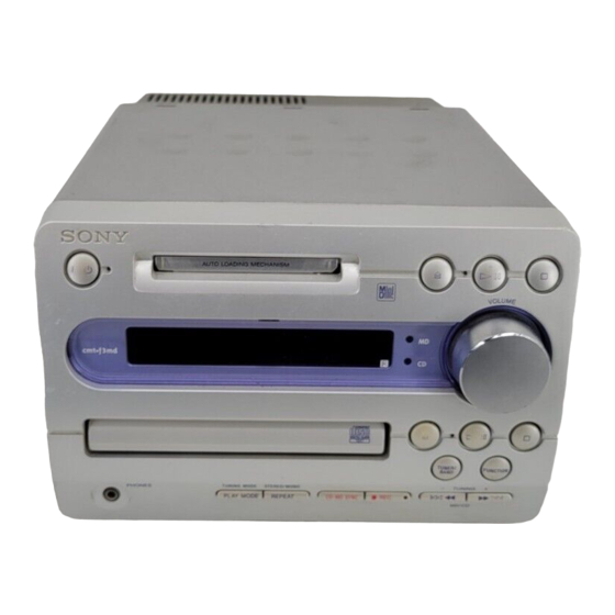
HCD-F3MD is the Amplifier, CD player, MD
Deck and Tuner section in CMT-F3MD.
US and foreign patents licensed from Dolby
Laboratories.
Amplifier section
DIN power output (Rated):20 + 20 watts (6 ohms at 1 kHz,
DIN, 240 V)
18 + 18 watts (6 ohms at 1 kHz,
DIN, 220 V)
Continuous RMS power output (Reference):
25 + 25 watts (6 ohms at 1 kHz,
10% THD, 240 V)
23 + 23 watts (6 ohms at 1 kHz,
10% THD, 220 V)
Peak Music Power Output: 400 watts
Inputs
TAPE IN (phono jacks):
voltage 250 mV, impedance
47 kilohms
Outputs
TAPE OUT (phono jacks): voltage 250 mV, impedance
1 kilohm
PHONES (stereo minijack):
accepts headphones of 8 ohms or
more.
SPEAKER:
accepts impedance of 6 to 16
ohms.
CD player section
System
Compact disc and digital audio
system
Laser
Semiconductor laser (λ=780 nm)
Emission duration: continuous
HCD-F3MD
Model Name Using Similar Mechanism
CD
CD Mechanism Type
Section
Base Unit Name
Optical Pick-up Name
Model Name Using Similar Mechanism
MD
MD Mechanism Type
Section
Base Unit Name
Optical Pick-up Name
SPECIFICATIONS
Max. 44.6 µW*
Laser output
*This output is the value measured
at a distance of 200 mm from the
objective lens surface on the
Optical Pick-up Block with a
7 mm aperture.
Frequency response
2 Hz – 20 kHz
MD deck section
System
MiniDisc digital audio system
Laser
Semiconductor laser (λ=780 nm)
Emission duration: continuous
Max. 44.6 µW*
Laser output
*This output is the value measured
at a distance of 200 mm from the
objective lens surface on the
Optical Pick-up Block with a
7 mm aperture.
Sampling frequency
44.1 kHz
Frequency response
5 Hz – 20 kHz
Tuner section
FM stereo, FM/AM superheterodyne tuner
FM tuner section
Tuning range
87.5 – 108.0 MHz
(50 kHz step)
Aerial
FM lead aerial
Aerial terminals
75 ohms unbalanced
Intermediate frequency
10.7 MHz
COMPACT DISC DECK RECEIVER
E Model
HCD-MD373
CDM55A-5SBD32
BU-5SBD32
KSS-213BH/Z-NP
HCD-MD373
MDM-5GA
MBU-5A
KMS-260B/S1NP
AM tuner section
Tuning range
531 – 1,602 kHz
(with the interval set at 9 kHz)
530 – 1,710 kHz
(with the interval set at 10 kHz)
Aerial
AM loop aerial
External aerial terminals
Intermediate frequency
450 kHz
General
Power requirements
110 – 120 V or 220 – 240 V
AC, 50/60 Hz
Power consumption
70 watts during normal operation
Approx. 3 watts in standby mode
(clock displayed)
Approx. 1 watt in standby mode
(clock not displayed)
Dimensions (w/h/d) incl. projecting parts and controls
Approx. 215 × 150 × 335 mm
Mass
Approx. 4.9 kg
Design and specifications are subject to change
without notice.
Advertisement
Table of Contents

Related Manuals for Sony HCD-F3MD


Summary of Contents for Sony HCD-F3MD
- Page 1 HCD-F3MD SERVICE MANUAL E Model HCD-F3MD is the Amplifier, CD player, MD Deck and Tuner section in CMT-F3MD. US and foreign patents licensed from Dolby Model Name Using Similar Mechanism HCD-MD373 Laboratories. CD Mechanism Type CDM55A-5SBD32 Section Base Unit Name...
-
Page 2: Self-Diagnosis Function
To solve the problem refer to the the beginning. following list. If any problem persists, consult C13/Read Error your nearest Sony dealer. The MD deck cannot read the disc information properly. cRemove the MD once, then insert it again. - Page 3 ITEMS OF ERROR HISTORY MODE ITEMS AND CONTENTS Selecting the Test Mode Display Details of History total rec Displays the recording time. Displayed as “rssssssh”. The displayed time is the total time the laser is set to the high power state. This is about 1/4 of the actual recording time.
-
Page 4: Table Of Contents
LINE WITH MARK 0 ON THE SCHEMATIC DIAGRAMS AND IN THE PARTS LIST ARE CRITICAL TO SAFE OPERATION. REPLACE THESE COMPONENTS WITH SONY PARTS WHOSE PART NUMBERS APPEAR AS SHOWN IN THIS MANUAL OR IN SUPPLEMENTS PUB- LISHED BY SONY. -
Page 5: Servicing Notes
SECTION 1 SERVICING NOTES MODEL IDENTIFICATION NOTES ON HANDLING THE OPTICAL PICK-UP BLOCK OR BASE UNIT — Back panel — The laser diode in the optical pick-up block may suffer electro- static break-down because of the potential difference generated PART No. by the charged electrostatic load, etc. - Page 6 DRAWING OUT THE TRAY WHEN THE POWER IS OFF tray (CDM) Move the cam block in the direction of arrow A with a finger. CLEANING THE OPTICAL PICK-UP (CD PLAYER) CD mechanism deck floating screw (PTPWH M2.6) optical pick-up block Clean the lens block with a cotton bud.
- Page 7 SERVICE POSITION OF THE MD MECHANISM SERVICE POSITION OF THE CD MECHANISM DECK DECK MD mechanism deck CD mechanism deck SERVICE POSITION OF THE POWER BOARD POWER board AMP board CN802 CN993 MAIN board Extension cable (4P) (J-2501-042-A) Extension cable (3P) (J-2501-045-A)
- Page 8 MC COLD RESET • The cold reset clears all data including preset data stored in the RAM to initial conditions. Execute this mode when returning the set to the customer. Procedure: 1. Press the button to turn the power on. [PLAY MODE/TUNING MODE] 2.
- Page 9 MD SECTION JIG FOR CHECKING BD (MD) BOARD WAVEFORM The special jig (J-2501-149-A) is useful for checking the waveform of the BD (MD) board. The names of terminals and the checking items to be performed are shown as follows. GND : Ground I+3V : For measuring IOP (Check the deterioration of the optical pick-up laser) IOP : For measuring IOP (Check the deterioration of the optical pick-up laser) TEO : Tracking error signal (Traverse adjustment)
- Page 10 Note : About “R” As this unit has only a few buttons, some operations require the use of remote commander (RM-SF3MD/provided with unit: 1-476-068-11) buttons. These operations are indicated as “R” in this manual. [MENU/NO] Example: ...Press the button of the remote commander. MENU/NO “R”...
- Page 11 CHECKS PRIOR TO PARTS REPLACEMENT AND ADJUSTMENTS Before performing repairs, perform the following checks to determine the faulty locations up to a certain extent. Details of the procedures are described in “5 Electrical Adjustments”. Criteria for Determination Measure if unsatisfactory: (Unsatisfactory if specified value is not satisfied) Laser power check •...
- Page 12 RETRY CAUSE DISPLAY MODE • In this test mode, the causes for retry of the unit during recording can be displayed on the fluorescent indicator tube. During playback, the “track mode” for obtaining track information will be set. This is useful for locating the faulty part of the unit. •...
- Page 13 Reading the Retry Cause Display Higher Bits Lower Bits Hexa- Details Hexadecimal decimal When 0 When 1 b7 b6 b5 b4 b3 b2 b1 b0 Binary Emphasis OFF Emphasis ON Monaural Stereo This is 2-bit display. Normally 01. 01:Normal audio. Others:Invalid Audio (Normal) Invalid Original...
- Page 14 CD SECTION CD TEXT DISPLAY • This unit displays CD text. Text is displayed for the first 50 tracks only and will not be displayed from the 51st track onwards. Do not suspect a fault in this case. In some cases, some special characters will not be displayed and may be replaced by other characters. Do not suspect a fault in this case. AGING MODE •...
- Page 15 • Reading the Mechanism Error History Display [PLAY MODE/TUNING MODE] (To switch the history, press the button) Display E@@M @@ : Error number. 00 is the latest : Invalid : Load in operations related D : Operations stopped due to problems other than mechanism related during CLOSE E : Operations stopped due to problems other than mechanism related during OPEN C : Operations stopped due to problems other than mechanism related during chucking up : Load out operations related...
-
Page 16: General
SECTION 2 This section is extracted from GENERAL instruction manual. LOCATION OF CONTROLS • Front View 1 I/1 button and indicator 2 MD disc slot 3 MD A button and MD disc indicator 4 MD H S button and indicator 5 MD s button 6 CD disc tray 7 CD A button and CD disc indicator... - Page 17 3 N (play) button 9 DBFB button Parts descriptions for Press to reinforce the bass sound. (page 44) X (pause) button the remote 0 SCROLL button x (stop) button Press to display the disc title or track title CURSORT/t, m/M buttons scrolling.
-
Page 18: Disassembly
SECTION 3 DISASSEMBLY Note: Follow the disassembly procedure in the numerical order given. CASE 2 case 1 two screws (case3 TP2) 1 two screws (case3 TP2) FRONT PANEL SECTION 3 Remove the cord. 5 screw (BVTT3 × 6) 9 MD mechanism deck section 8 screw 8 screw (BVTP2.6 ×... - Page 19 MD MECHANISM DECK (MDM-5GA) 2 four step screws (BVTPWH M3) 1 connector (CN601) 6 MD mechanism deck (MDM-5GA) 4 wire (flat type) (23 core) (CN103) 4 wire (flat type) (21 core) (CN102) 5 bracket (MDM) SLIDER (CAM) 7 slider (cam) •...
- Page 20 BD (MD) BOARD, BASE UNIT (MBU-5A) 5 two flexible boards (CN101, 104) 7 base unit (MBU-5A) 1 Remove two solders CN103 CN102 of spindle motor leads (M901). 6 BD (MD) board 4 screw (M1.7) 2 Remove two solders of sled motor leads (M902). 3 three screws (DIA.2.6) OVER WRITE HEAD (HR901)
- Page 21 SPINDLE MOTOR ASS’Y (M901), SLED MOTOR ASS’Y (M902) 4 three screws (B2 × 5) 3 gear (SL-B) 1 screw (M1.7) 2 gear (SL-A) 5 spindle motor ass’y (M901) 6 two screws (P1.7 × 2.5) 7 sled motor ass’y (M902) OPTICAL PICK-UP OF MD (KMS-260B/S1NP) 4 Turn over the optical pick-up.
- Page 22 BACK PANEL ASS’Y 4 back panel ass’y 1 six screws (BVTP3 × 10) 3 claw 3 claw 2 claw SP BOARD, POWER BOARD AND MAIN BOARD 4 two connectors 4 connector (CN993) (CN991, 992) 5 two screws (BVTT3 × 6) 8 connector 3 wire (flat type) (25 core) (CN994)
- Page 23 CD MECHANISM DECK (CDM55A-5SBD32) 4 holder (MDM) 3 screw (BVTT3 × 6) 7 CD mechanism deck (CDM55A-5SB32) 5 screw (BVTT3 × 6) 1 wire (flat type) (19 core) 6 two claws (CN109) 3 screw (BVTT3 × 6) 2 connector (CN110) TRAY (CDM), GEAR AND CAM (CDM55) 4 belt (CDM55) Note: when drawing out the tray (CDM), refer to...
- Page 24 HOLDER (BU) ASS’Y 1 floating screw (PTPWH M2.6) 2 Remove the holder (BU) ass’y in the direction of the arrow. OPTICAL PICK-UP OF CD (KSS-213BH/Z-NP) 5 optical pick-up (KSS-213BH/Z-NP) 3 wire (flat type) (16 core) 1 Release the lever in the direction of arrow A .
- Page 25 BD (CD) BOARD, BASE (BU-5S) ASS’Y (M101) AND SLED MOTOR ASS’Y (M102) 4 two screws (B2 × 4) 6 gear (M) 9 base (BU-5S) ass’y (M101) 8 two insulators (BU) 2 Remove the four solders. 8 two insulators (BU) 7 flatness gear M101 5 sled motor ass’y M102...
-
Page 26: Test Mode
SECTION 4 TEST MODE Note : About “R” As this unit has only a few buttons, some operations require the use of remote commander (RM-SF3MD/provided with unit: 1-476-068-11) buttons. These operations are indicated as “R” in this manual. [MENU/NO] Example: ...Press the button of the remote commander. - Page 27 4-5. SELECTING THE TEST MODE There are 31 types of test modes as shown below. The groups can be switched by pessing the button. After selecting the group to be used, press the button. After setting a certain group, press the button ENTER/YES “R”...
- Page 28 4-5-1. Operating the Continuous Playback Mode 1. Entering the continuous playback mode (1) Set the disc in the unit. (Whichever recordable discs or discs for playback only are available.) (2) Press the button and display “CPLAY MODE”. (3) Press the button to change the display to “CPLAY MID”.
- Page 29 4-7. TEST MODE DISPLAYS Each time the button is pressed, the display changes in the following order. DISP “R” 1. Mode display Displays “TEMP ADJUST”, “CPLAYMODE”, etc. 2. Error rate display Displays the error rate in the following way. C1 = ssss AD = ss C1 = Indicates the C1 error.
-
Page 30: Electrical Adjustments
SECTION 5 ELECTRICAL ADJUSTMENTS MD SECTION 5-1. PARTS REPLACEMENT AND ADJUSTMENT • Check and adjust the mechanism deck as follows. • Abbreviation The procedure changes according to the part replaced : Optical pick-up OWH : Overwrite head • Temperature compensation offset check •... - Page 31 Note : About “R” As this unit has only a few buttons, some operations require the use of remote commander (RM-SF3MD/provided with unit: 1-476-068-11) buttons. These operations are indicated as “R” in this manual. [MENU/NO] Example: ...Press the button of the remote commander. MENU/NO “R”...
- Page 32 5-6. CHECK PRIOR TO REPAIRS Note 1: After step 4, each time the button is pressed, ENTER/YES “R” the display will be switched “LD 0.7 mW $ ”, “LD 6.2 mW $ These checks are performed before replacing parts according to ”, and “LD Wp ”.
- Page 33 5-6-5. C PLAY Check 9. Press the button to display “EFB = MO-P”. ENTER/YES “R” Then, the optical pick-up moves to the pit area automatically MO Error Rate Check and servo is imposed. 10. Observe the waveform of the oscilloscope, and check that the Checking Procedure : specified value is satisfied.
- Page 34 5-8. RECORDING AND DISPLAYING THE IOP 5-10. LASER POWER ADJUSTMENT INFORMATION Check the IOP value of the optical pick-up before adjustments. (Refer to 8. Recording and Displaying IOP Information) The IOP data can be recorded in the non-volatile memory. The IOP value on the optical pick-up label and the IOP value after the Connection : adjustment will be recorded.
- Page 35 12. Press the button. When the display becomes 7. Press the button and save the result of adjust- ENTER/YES “R” ENTER/YES “R” Ref=@@@.@ (@ is an arbitrary number), press the ment to the non-volatile memory (“EFB = SAVE” will be ENTER/ button to display “Measu=@@@.@”...
- Page 36 5-13-2. MO Error Rate Check 18. Press the button, display “EFB = SAVE” ENTER/YES “R” for a moment and save the adjustment results in the non-volatile Checking Procedure : memory. 1. Load the continuously-recorded disc. (Refer to “5-5. CRE- Next “EF CD ADJUST” will be displayed. ATING CONTINUOUSLY-RECORDED DISC”) 19.
- Page 37 5-15-2. MO Auto Gain Control Output Level Adjustment Adjustment Location: Adjusting Procedure : – BD (MD) BOARD (Side A) – 1. Load the test disc (MDW-74/AU-1). 2. Press the button to display “AG Set CN101 (MO)”. 3. When the button is pressed, the adjustment ENTER/YES “R”...
-
Page 38: Cd Section
Note: Clear RF signal waveform means that the shape “◊” can be clearly CD SECTION distinguished at the center of the waveform. Note : RF signal waveform 1. CD Block is basically designed to operate without adjustment. Therefore, check each item in order given. VOLT/DIV : 200 mV 2. -
Page 39: Diagrams
HCD-F3MD SECTION 6 DIAGRAMS 6-1. BLOCK DIAGRAM – CD SERVO Section – FILTER DIGITAL SIGNAL PROCESSOR, DIGITAL FILTER, D/A CONVERTER, DIGITAL SERVO PROCESSOR OPTICAL PICK-UP BLOCK IC101 (KSS-213BH/Z-NP) XTA1 IC103 DETECTOR TIMING X101 RF AMP, LOGIC 16.9344MHz FOCUS/TRACKING ERROR AMP... -
Page 40: Block Diagram - Md Servo Section (1/2)
HCD-F3MD 6-2. BLOCK DIAGRAM – MD SERVO Section (1/2) – DIGITAL SERVO SIGNAL PROCESSOR, DIGITAL SIGNAL PROCESSOR EFM/ACIRC ENCODER/DECODER, SHOCK-PROOF MEMORY CONTROLLER, OVER WRITE HEAD DRIVE ATRAC ENCODER/DECODER IC181 IC121 HR901 OVER WRITE • DIN0 LEVEL SHIFT HEAD DOUT IC202 (1/2) •... -
Page 41: Block Diagram - Md Servo Section (2/2)
HCD-F3MD 6-3. BLOCK DIAGRAM – MD SERVO Section (2/2) – A/D,D/A CONVERTER IC201 MD REC-L DATAO VINL1 (AD IN L) VINR1 R-CH MD-L VOUTL (DATA OUT L) VOUTR R-CH ADDT MD LEVEL-L LRCK DADT DATAI L3MODE L3CLK X201 512FS OSC... -
Page 42: Block Diagram - Main Section
HCD-F3MD 6-4. BLOCK DIAGRAM – MAIN Section – MUTING CONTROL MUTING Q551 Q841 RY881 1 POWER AMP IC801 R-CH TUNER UNIT TM881 – ANTENNA DBFB SW SPEAKER DBFB DET RELAY DRIVE Q301 D881 Q881 IMPEDANCE STEREO – 6 – 16Ω... -
Page 43: Note For Printed Wiring Boards And Schematic Diagrams
• Circuit Boards Location 6-5. NOTE FOR PRINTED WIRING BOARDS AND SCHEMATIC DIAGRAMS (In addition to this, the necessary note is printed in each block) Note on Schematic Diagram: Note on Printed Wiring Boards: AMP board • X : parts extracted from the component side. •... -
Page 44: Printed Wiring Board - Bd (Cd) Board
HCD-F3MD 6-6. PRINTED WIRING BOARD – BD (CD) Board – • See page 43 for Circuit Boards Location. TP(VC) TP(RF) (Page 52) TP(AGCCON) MAIN BOARD CN109 TP(FE) TP(TE) TP(FE1) OPTICAL PICK-UP BLOCK KSS-213BH/Z-NP... -
Page 45: Schematic Diagram - Bd (Cd) Board
HCD-F3MD 6-7. SCHEMATIC DIAGRAM – BD (CD) Board – • • See page 62 for waveforms. See page 63 for IC Block Diagrams. TP (VC) TP (RF) RF AMP, FOCUS/TRACKING ERROR AMP TP (TE) TP (FE) Q101 AUTOMATIC POWER CONTROL... -
Page 46: Schematic Diagram - Bd (Md) Board (1/2)
HCD-F3MD 6-8. SCHEMATIC DIAGRAM – BD (MD) Board (1/2) – • • See page 62 for waveforms. See page 63 for IC Block Diagrams. • Voltages and waveforms are dc with respect to ground OPTICAL PICK-UP BLOCK (KMS-260B/S1NP) under no-signal conditions. -
Page 47: Schematic Diagram - Bd (Md) Board (2/2)
HCD-F3MD 6-9. SCHEMATIC DIAGRAM – BD (MD) Board (2/2) – • See page 62 for waveforms. • See page 63 for IC Block Diagrams. BD (MD) BOARD (1/2) (Page 46) MD DIGITAL BOARD CN104 DIVIDER (Page 51) PIN FUNCTION MD DIGITAL... -
Page 48: Printed Wiring Board - Bd (Md) Board
HCD-F3MD 6-10. PRINTED WIRING BOARD – BD (MD) Board – • See page 43 for Circuit Boards Location. • Semiconductor • Semiconductor Location Location (Page 50) (Page 50) Ref. No. Location Ref. No. Location D101 IC101 D181 IC121 D183 IC124... -
Page 49: Schematic Diagram - Bd Sw (Md) Board
HCD-F3MD 6-11. SCHEMATIC DIAGRAM – BD SW (MD) Board – 6-13. SCHEMATIC DIAGRAM – LOADING (CD) Board – CD TRAY CN151 OPEN/CLOSE DETECT CLOSE MD DIGITAL CLOSE BOARD CN102 OPEN OPEN (Page 51) LOAD + MAIN BOARD (3/3) LOAD –... -
Page 50: Printed Wiring Board - Md Digital Board
HCD-F3MD 6-15. PRINTED WIRING BOARD – MD DIGITAL Board – • See page 43 for Circuit Boards Location. BOARD CN601 (Page 49) BD(MD) BOARD CN102 (Page 48) BD(MD) BOARD(2/2) CN103 (Page 48) (Page 52) MAIN BOARD CN107... -
Page 51: Schematic Diagram - Md Digital Board
HCD-F3MD 6-16. SCHEMATIC DIAGRAM – MD DIGITAL Board – • • See page 62 for waveforms. See page 63 for IC Block Diagrams. (Page 54) • Voltages and waveforms are dc with respect to ground under no-signal conditions. no mark : MD STOP ) : MD PLAY <... -
Page 52: Printed Wiring Board - Main Board
HCD-F3MD 6-17. PRINTED WIRING BOARD – MAIN Board – • See page 43 for Circuit Boards Location. (Page 50) (Page 44) • Semiconductor Location (Page 56) Ref. No. Location D171 D901 D911 D912 D913 D914 D921 D922 D923 D924 D941... -
Page 53: Schematic Diagram - Main Board (1/3)
HCD-F3MD 6-18. SCHEMATIC DIAGRAM – MAIN Board (1/3) – • See page 63 for IC Block Diagrams. (Page 57) • Voltages and waveforms are dc with respect to ground (Page 55) (Page 54) (Page 54) (Page 55) (Page 54) under no-signal (detuned) conditions. -
Page 54: Schematic Diagram - Main Board (2/3)
HCD-F3MD 6-19. SCHEMATIC DIAGRAM – MAIN Board (2/3) – • See page 63 for IC Block Diagrams. (Page 53) (Page 53) (Page 53) (Page 61) (Page 51) (Page 55) (Page 55) (Page 55) (Page 55) (Page 55) (Page 55) • Voltages and waveforms are dc with respect to ground under no-signal (detuned) conditions. -
Page 55: Schematic Diagram - Main Board (3/3)
HCD-F3MD 6-20. SCHEMATIC DIAGRAM – MAIN Board (3/3) – • • See page 62 for Waveforms. See page 63 for IC Block Diagrams. (Page 54) (Page 53) (Page 54) (Page 54) (Page 54) (Page 54) (Page 53) (Page 54) (Page 45) -
Page 56: Printed Wiring Boards - Amp/Sp Boards
HCD-F3MD 6-21. PRINTED WIRING BOARDS – AMP/SP Boards – • See page 43 for Circuit Boards Location. • Semiconductor Location Ref. No. Location D801 D802 D832 D851 D852 IC801 Q801 Q802 Q841 Q851 Q852 Q871 Q872 Q873 (Page 52) (Page 60) There are a few cases that the part isn't mounted in model is printed on diagrams. -
Page 57: Schematic Diagram - Amp/Sp Boards
HCD-F3MD 6-22. SCHEMATIC DIAGRAM – AMP/SP Boards – (Page 61) • Voltages and waveforms are dc with respect to ground The components identified by mark 0 or dotted under no-signal (detuned) conditions. line with mark 0 are critical for safety. -
Page 58: Printed Wiring Board - Panel Board
HCD-F3MD 6-23. PRINTED WIRING BOARD – PANEL Board – • See page 43 for Circuit Boards Location. • Semiconductor Location Ref. No. Location D661 D663 D664 D665 D667 D668 IC601 IC602 Q601 Q661 Q662 Q663 Q664 Q665 FL601 Q666 FLUORESCENT INDICATOR TUBE... -
Page 59: Schematic Diagram - Panel Board
HCD-F3MD 6-24. SCHEMATIC DIAGRAM – PANEL Board – • • See page 62 for Waveform. See page 63 for IC Block Diagram. (Page 55) • Voltages and waveforms are dc with respect to ground under no-signal (detuned) conditions. no mark : TUNER... -
Page 60: Printed Wiring Board - Power Board
HCD-F3MD 6-25. PRINTED WIRING BOARD – POWER Board – • See page 43 for Circuit Boards Location. (Page 52) • Semiconductor Location Ref. No. Location D971 D972 D973 D974 D975 D976 D977 D978 D979 D980 D981 D982 D983 D984 D985... -
Page 61: Schematic Diagram - Power Board
HCD-F3MD 6-26. SCHEMATIC DIAGRAM – POWER Board – (Page 57) (Page 54) • Voltages and waveforms are dc with respect to ground The components identified by mark 0 or dotted under no-signal (detuned) conditions. line with mark 0 are critical for safety. - Page 62 • Waveforms – BD (CD) Board – – BD (MD) Board – – MD DIGITAL Board – – MAIN Board – – PANEL Board – 1 IC101 yh (XTAI) 1 IC101 1, 2 (I, J) (MD play mode) 6 IC121 wk (XBCK) 1 IC202 9 1 IC501 q;...
- Page 63 • IC Block Diagrams – BD (CD) Board – IC101 CXD2587Q ERROR DIGITAL CORRECTOR DIGITAL ASYMMETRY CORRECTION OPERATIONAL LRCK AMPLIFIER ANALOG SWITCH PCMD INTERFACE DEMODULATOR CONVERTER EMPH XVDD XTAI TIMING CLOCK LOGIC XTAO XTSL GENERATOR XVSS TES1 AVDD1 TEST AOUT1 SERVO DSP PWM GENERATOR AIN1...
- Page 64 IC103 CXA2568M-T6 HOLD APC PD AMP LC/PD APC LD AMP – LD ON – – – HOLD SW AGC CONT AGC VTH 50µA RF BOT – – – – RFTC RF SUMMING AMP RF EQ AMP RF I RF O –...
- Page 65 – BD (MD) Board – IC101 CXA2523AR 43 42 USROP – RF AGC – USRC RFA1 BPF3T RFA2 RFA3 PEAK3T – HLPT –1 – – –2 – OFST PTGR TEMP PEAK – –2 – 36 BOTM BOTTOM – –1 GRVA PBSW 35 ABCD 34 FE...
- Page 66 IC121 CXD2654R 100 99 98 97 96 95 94 93 92 91 90 89 88 87 86 85 84 83 82 81 80 79 78 77 76 SPINDLE GENERATOR SERVO 75 TE MNT0 74 SE MNT1 EACH MONITOR 73 AVSS CONTROL BLOCK MNT2...
- Page 67 – MD DIGITAL Board – IC153 LB1830M-S-TE-L IC201 UDA1341TS VREF VCONT VREF VINL2 VINR2 LOGIC 0DB/6DB 0DB/6DB ADC2R ADC2L VINL1 VINR1 PREDRIVER SWITCH SWITCH ADC1L ADC1R AGCSTAT VDDD DIGITAL AGC VSSD DIGITAL MIXER DECIMATION FILTER OVERFLOW DATAO L3CLOCK DIGITAL L3-BUS L3MODE INTERFACE INTERFACE...
- Page 68 – MAIN Board – IC301 M62428AFP600C AVDD VREF REF AMP AGND – VREFI VREFO SUR R SURROUND SW MIC IN AGND SUR C IN1A IN2A IN1B – IN2B IN1C BUFF BUFF AMP1 AMP2 IN2C IN1D IN2D AMP1 AMP2 REC OUT1 REC OUT2 INBAS1 INBAS2...
- Page 69 IC171 LB1641 IC931 M62016L T.S.D O.C.P INTERRUPT SIGNAL MOTOR MOTOR – GENERATING BLOCK DRIVE DRIVE RESET SIGNAL GENERATING BLOCK – FWD/REV/STOP CONTROL LOGIC RESET – PANEL Board – IC601 M66004M8FP DIG11 DIG12 DIGITAL OUTPUT DIG0 DIG15 CIRCUIT INDICATION CONTROLLER SERIAL RECEIVE CIRCUIT DATA...
-
Page 70: Ic Pin Function Description
6-27. IC PIN FUNCTION DESCRIPTION • BD (MD) BOARD IC101 CXA2523AR (RF AMP, FOCUS/TRACKING ERROR AMP) Pin No. Pin Name Description I-V converted RF signal I input from the optical pick-up block detector I-V converted RF signal J input from the optical pick-up block detector Middle point voltage (+1.65V) generation output terminal 4 to 9 A to F... - Page 71 • BD (MD) BOARD IC121 CXD2654R (DIGITAL SIGNAL PROCESSOR, DIGITAL SERVO PROCESSOR, EFM/ACIRC ENCODER/DECODER, SHOCK PROOF MEMORY CONTROLLER, ATRAC ENCODER/DECODER) Pin No. Pin Name Description Focus OK signal output to the MD mechanism controller (IC316) MNT0 (FOK) “H” is output when focus is on (“L”: NG) MNT1 (SHOCK) Track jump detection signal output to the MD mechanism controller (IC316) MNT2 (XBUSY)
- Page 72 Pin No. Pin Name Description Address signal output to the D-RAM (IC124) XRAS Row address strobe signal output to the D-RAM (IC124) “L” active Write enable signal output to the D-RAM (IC124) “L” active Two-way data bus with the D-RAM (IC124) I (S) MVCI Digital in PLL oscillation input from the external VCO Not used (fixed at “L”)
- Page 73 Pin No. Pin Name Description FRDR Focus servo drive PWM signal (–) output to the BH6511FS (IC152) Clock signal (176.4 kHz) output terminal (X’tal system) Not used (open) SRDR Sled servo drive PWM signal (–) output to the BH6511FS (IC152) SFDR Sled servo drive PWM signal (+) output to the BH6511FS (IC152) SPRD...
- Page 74 • MD DIGITAL BOARD IC316 M30624MG-A16FP (MD MECHANISM CONTROLLER) Pin No. Pin Name Description WMOUT Serial data output to the equipment connected to other unit Not used (open) Serial data transfer clock signal input from the equipment connected to other unit WMCLK Not used (fixed at “L”) LEVEL-L...
- Page 75 Pin No. Pin Name Description Over write head up/down motor control signal output terminal HEADUP “H” active Not used (open) JOG0 Jog dial pulse input terminal (A phase input) Not used (open) JOG1 Jog dial pulse input terminal (B phase input) Not used (open) Clock signal phase inversion control signal output to the equipment connected to other unit WMINV Not used (open)
- Page 76 Pin No. Pin Name Description XLATCH Serial data latch pulse signal output to the CXD2654R (IC121) Laser power select signal output to the CXD2654R (IC121) and HF module switch circuit WRPWR “L”: playback mode, “H”: recording mode LOADING Setting terminal for the loading control method SEL: L “H”: not used IN switch (fixed at “L”) L3MODE...
- Page 77 • MAIN BOARD IC501 M30620MCA-A51FP (MASTER CONTROLLER) Pin No. Pin Name Description STKPOWER Power amplifier (IC801) on/off selection signal output terminal “H”: power amplifier on Power on/off control signal output terminal Not used (open) F-RY Speakers on/off relay (RY881) drive signal output terminal “H”: speakers on R-RY Rear speakers on/off relay drive signal output terminal “H”: speakers on Not used (open) CD-POWER...
- Page 78 Pin No. Pin Name Description OPT-SEL Optical signal selection signal output terminal Not used (open) 62DATA Serial data output to the M62428AFP (IC301) 62CLK Serial data transfer clock signal output to the M62428AFP (IC301) ST-MUTE Tuner muting control signal output to the tuner pack “L”: muting on STEREO FM stereo detection signal input from the tuner pack TUNED...
- Page 79 Pin No. Pin Name Description Key input terminal (A/D input) S603 to 608 (CDs, CDHS, CDA, MDs, MDHS, MDA, KEY1 keys input) Key input terminal (A/D input) S609 to 616 (FUNCTION, +M L, TUNER/BAND, –l KEY2 m, z REC, CD-MD SYNC, STEREO/MONO REPEAT, TUNING MODE/PLAY MODE keys input) MD-REC-R R-ch level input from the MD mechanism controller (IC316)
-
Page 80: Exploded Views
SECTION 7 EXPLODED VIEWS NOTE: • -XX and -X mean standardized parts, so they • Items marked “*” are not stocked since they The components identified by mark 0 or dotted line with mark may have some difference from the original are seldom required for routine service. - Page 81 (2) CHASSIS SECTION T900 not supplied T901 not supplied CDM55A-5SBD32 not supplied not supplied The components identified by mark 0 or dotted line with mark 0 are critical for safety. Replace only with part number specified. Ref. No. Part No. Description Remark Ref.
- Page 82 (3) MD MECHANISM DECK SECTION (MDM-5GA) not supplied M903 MBU-5A Ref. No. Part No. Description Remark Ref. No. Part No. Description Remark * 101 1-671-115-21 SW BOARD 4-996-227-14 LEVER (HEAD) * 102 4-996-217-01 CHASSIS 4-996-229-01 SPRING (HEAD LEVER), TORSION * 104 4-996-218-01 BRACKET (GUIDE R) 4-998-763-14 SPRING (SHUTTER), LEAF 4-996-277-01 SPRING (O/C), TENSION...
- Page 83 (4) MD BASE UNIT SECTION (MBU-5A) HR901 not supplied not supplied S102 M901 M902 The components identified by mark 0 or dotted line with mark 0 are critical for safety. Replace only with part number specified. Ref. No. Part No. Description Remark Ref.
- Page 84 (5) CD MECHANISM DECK SECTION (CDM55A-5SBD32) not supplied M103 not supplied (BU-5SBD32) not supplied Ref. No. Part No. Description Remark Ref. No. Part No. Description Remark 4-925-315-31 DAMPER 4-221-916-01 BUSHING 1-674-336-12 LOADING BOARD A-4672-773-A PULLEY (AT) ASSY 4-220-231-01 TRAY (CDM) 4-985-672-01 SCREW (+PTPWH M2.6), FLOATING 4-220-229-01 LEVER (SW) 4-220-230-01 CHASSIS...
- Page 85 (6) CD BASE UNIT SECTION (BU-5SBD32) M102 M101 (including z C) The components identified by mark 0 or dotted line with mark 0 are critical for safety. Replace only with part number specified. Ref. No. Part No. Description Remark Ref. No. Part No.
-
Page 86: Electrical Parts List
SECTION 8 ELECTRICAL PARTS LIST NOTE: • Due to standardization, replacements in the • Items marked “*” are not stocked since they The components identified by mark 0 or dotted line with mark are seldom required for routine service. parts list may be different from the parts speci- 0 are critical for safety. - Page 87 BD (CD) Ref. No. Part No. Description Remark Ref. No. Part No. Description Remark R845 1-249-441-11 CARBON 100K 1/4W C157 1-163-009-11 CERAMIC CHIP 0.001uF R851 1-249-421-11 CARBON 2.2K 1/4W C159 1-163-019-00 CERAMIC CHIP 0.0068uF 10% R852 1-249-429-11 CARBON 1/4W C161 1-126-206-11 ELECT CHIP 100uF 6.3V...
- Page 88 BD (CD) BD (MD) Ref. No. Part No. Description Remark Ref. No. Part No. Description Remark R147 1-216-069-00 METAL CHIP 6.8K 1/10W C135 1-163-038-11 CERAMIC CHIP 0.1uF R148 1-216-001-00 METAL CHIP 1/10W R149 1-216-001-00 METAL CHIP 1/10W C136 1-126-206-11 ELECT CHIP 100uF 6.3V R158...
- Page 89 BD (MD) LOADING Ref. No. Part No. Description Remark Ref. No. Part No. Description Remark L105 1-414-813-11 FERRITE L106 1-414-813-11 FERRITE R149 1-216-073-00 METAL CHIP 1/10W R150 1-216-295-11 SHORT L121 1-414-813-11 FERRITE R151 1-216-073-00 METAL CHIP 1/10W L122 1-414-813-11 FERRITE R152 1-216-073-00 METAL CHIP 1/10W...
- Page 90 MAIN Ref. No. Part No. Description Remark Ref. No. Part No. Description Remark A-4475-919-A MAIN BOARD, COMPLETE (HK, TW) C363 1-126-957-11 ELECT 0.22uF A-4475-923-A MAIN BOARD, COMPLETE (KR) C364 1-130-473-00 MYLAR 0.0015uF 5% C365 1-124-721-11 ELECT 10uF ********************* C366 1-136-165-00 FILM 0.1uF 7-685-646-79 SCREW +BVTP 3X8 TYPE2 N-S C367...
- Page 91 MAIN Ref. No. Part No. Description Remark Ref. No. Part No. Description Remark D921 8-719-024-99 DIODE 11ES2-NTA2B D922 8-719-911-19 DIODE 1SS119-25 R132 1-247-807-31 CARBON 1/4W D923 8-719-911-19 DIODE 1SS119-25 R141 1-249-417-11 CARBON 1/4W D924 8-719-911-19 DIODE 1SS119-25 R151 1-249-441-11 CARBON 100K 1/4W R152...
- Page 92 MAIN MD DIGITAL Ref. No. Part No. Description Remark Ref. No. Part No. Description Remark R523 1-249-417-11 CARBON 1/4W R524 1-247-807-31 CARBON 1/4W R933 1-249-433-11 CARBON 1/4W R525 1-249-417-11 CARBON 1/4W R941 1-249-413-11 CARBON 1/4W R942 1-249-429-11 CARBON 1/4W R526 1-247-807-31 CARBON 1/4W R943...
- Page 93 MD DIGITAL PANEL Ref. No. Part No. Description Remark Ref. No. Part No. Description Remark < COIL > < CAPACITOR > L181 1-424-675-11 INDUCTOR 33uH C601 1-162-306-11 CERAMIC 0.01uF L201 1-500-445-21 FERRITE C602 1-162-306-11 CERAMIC 0.01uF L202 1-500-445-21 FERRITE C603 1-124-261-00 ELECT 10uF C604...
- Page 94 PANEL POWER Ref. No. Part No. Description Remark Ref. No. Part No. Description Remark < TRANSISTOR > S609 1-762-875-21 SWITCH, KEYBOARD (FUNCTION) S610 1-762-875-21 SWITCH, KEYBOARD Q601 8-729-620-05 TRANSISTOR 2SC2603-EF (TUNING +, MD/CD M L) Q661 8-729-900-63 TRANSISTOR DTA124ES Q662 8-729-900-63 TRANSISTOR DTA124ES S611...
- Page 95 8-719-911-19 DIODE 1SS119-25 0 F991 1-532-388-31 FUSE (T2AL/250V) (HK, TW) < COIL > < TRANSISTOR > L881 1-420-872-00 COIL, AIR-CORE Q971 8-729-018-59 TRANSISTOR 2SB1375 (LB-SONY) L882 1-420-872-00 COIL, AIR-CORE Q972 8-729-922-37 TRANSISTOR 2SD2144S-UVW Q973 8-729-922-37 TRANSISTOR 2SD2144S-UVW < TRANSISTOR >...
- Page 96 HCD-F3MD Ref. No. Part No. Description Remark Ref. No. Part No. Description Remark MISCELLANEOUS ************** 1-777-240-11 WIRE (FLAT TYPE) (21 CORE) 1-791-211-11 WIRE (FLAT TYPE) (23 CORE) 1-773-212-11 WIRE (FLAT TYPE) (25 CORE) 1-792-756-11 WIRE (FLAT TYPE) (29 CORE) 1-693-473-31 TUNER (FM/AM TUNER UNIT) (TW)
Need help?
Do you have a question about the HCD-F3MD and is the answer not in the manual?
Questions and answers