Sony HCD-V818 Service Manual
E model
Hide thumbs
Also See for HCD-V818:
- Service manual (19 pages) ,
- Service manual (92 pages) ,
- Service manual (18 pages)
Table of Contents
Advertisement
SERVICE MANUAL
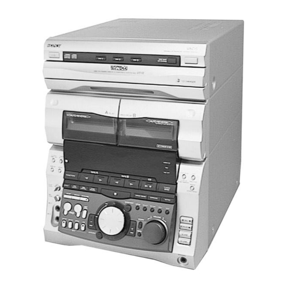
HCD-V818 is the tuner, deck, Video CD
and amplifier section in MHC-V818.
MICROFILM
HCD-V818
Model Name Using Similar Mechanism
CD
CD Mechanism Type
SECTION
Base Unit Type
Optical Pick-up Type
Model Name Using Similar Mechanism
TAPE
DECK
Tape Transport Mechanism Type
SECTION
SPECIFICATIONS
COMPACT DISC DECK RECEIVER
– 1 –
E Model
HCD-V800
CDM38L-5BD24AL
BU-5BD24AL
KSS-213D/Q-NP
HCD-GRX8/R800/RX88/RX99
TCM-230AWR1
TCM-230PWR1
— Continued on next page —
Advertisement
Table of Contents

Subscribe to Our Youtube Channel
Related Manuals for Sony HCD-V818


Summary of Contents for Sony HCD-V818
- Page 1 HCD-V818 SERVICE MANUAL E Model HCD-V818 is the tuner, deck, Video CD and amplifier section in MHC-V818. Model Name Using Similar Mechanism HCD-V800 CD Mechanism Type CDM38L-5BD24AL SECTION Base Unit Type BU-5BD24AL Optical Pick-up Type KSS-213D/Q-NP Model Name Using Similar Mechanism...
- Page 2 SELF DIAGNOSIS This unit is equipped with a self-diagnosis function. The function is used for diagnosing the conditions of the circuits of the VIDEO board. The circuits can be determined if normal or abnormal by the lighting of D502 of the VIDEO board. Lighting of D502 When lit : Operates normally...
- Page 3 REPLACE THESE COMPONENTS WITH SONY PARTS WHOSE PART NUMBERS APPEAR AS SHOWN IN THIS Carry out the “S curve check” in “CD section adjustment” and check MANUAL OR IN SUPPLEMENTS PUBLISHED BY SONY. that the S curve waveform is output two times. – 3 –...
-
Page 4: Table Of Contents
TABLE OF CONTENTS 1. SERVICING NOTE 9. EXPLODED VIEWS ............5 9-1. Case Section ................ 99 9-2. Chassis Section ..............100 2. GENERAL ................6 9-3. Front Panel Section ............101 9-4. CD Mechanism Deck Section-1 (CDM38L-5BD24AL) .. 102 3. DISASSEMBLY 9-5. -
Page 5: Servicing Note
SECTION 1 SERVICING NOTE HOW TO OPEN THE DISC TRAY WHEN POWER SWITCH TURNS OFF 1 Remove the case. 3 pull-out the disc tray. 2 Turn the cam to the direction of arrow. Note for Installation (ROTARY ENCODER) Note:When attaching the Base unit, Insert the BU cam section A into the groove of BU cam. -
Page 6: General
SECTION 2 GENERAL Front Panel 16 17 19 20 21 22 23 24 25 26 27 28 – 6 –... - Page 7 LOCATION OF PARTS AND CONTROLS 1 1/u (POWER) button 34 VOLUME, +, – knob 2 DISC 1 button and indicator 35 GROOVE button and indicator 3 DISC 2 button and indicator 36 DBFB button 37 ), + button and indicator 4 DISC 3 button and indicator 5 DISC SKIP/EX-CHANGE button 38 ENTER/NEXT button and indicator...
- Page 8 This section is extracted from instruction manual. – 8 –...
-
Page 9: Disassembly
SECTION 3 DISASSEMBLY Note: Follow the disassembly procedure in the numerical order given. 3-1. LOADING PANEL 3 Loading panel Claws 1 Turn the cam to the direction of arrow. 2 Pull-out the disc tray. 3-2. FRONT PANEL 6 Flat type wire (CN107) 7 Flat type wire (CN106) -
Page 10: Cassette Mechanism Deck
3-3. CASSETTE MECHANISM DECK 9 Three screws (BVTP 2.6x8) !∞ Mechanism deck !º Two screws (BVTP 2.6x8) 2 Two screws 6 Remove the cassette lids. (BVTT 2x4) !£ Two screws (BVTP 2.6x8) 4 Damper, oil 3 Damper, oil 1 Two screws (BVTT 2x4) 7 Spring !¢... -
Page 11: Disc Tray
3-5. DISC TRAY (Perfom after removing the front panel.) Note: When installing the Disc tray, pull around the flat type wire to pass through the clawA and clawB, as shown in the figure. 3 Flat type wire (8 core) 4 Two claws 2 Pull-out the disc tray. -
Page 12: Test Mode
SECTION 4 TEST MODE VIDEO CD COLOR-BARS MODE On this mode, the data of the color-bars signal as a picture signal and the 1kHz sine wave signal as a sound signal are output by the mechanism control microcomputer (IC502) for video CD signal check. When measurement of the voltage and waveform on the VIDEO board, perform it in this mode. - Page 13 IC502 OF VIDEO BOARD IC502 of the VIDEO board consists of the former type and new type. The following table shows the differences between the two types. Only spare parts for the new type IC502 are supplied. Units using the former IC502 will not function when replaced with the new type without performing the following procedure. Consequently, replace IC502 of units using the former type according to the following procedure.
-
Page 14: Service Mode
SECTION 5 SERVICE MODE MC Cold Reset • The cold reset clears all data including preset data stored in the RAM to initial conditions. Execute this mode when returning the set to the customer. Procedure: 1. Press three buttons p , ENTER/NEXT , and 1/u simultaneously. 2. - Page 15 Setting the aging mode: Press the p button, ENTER/NEXT button, and DISC SKIP/EX-CHANGE button together. When the aging mode is set, the CD roulette mark blinks. To exit the mode, press the 1/u button and turn OFF the power. Sequence: The aging mode is executed in the following sequence.
-
Page 16: Mechanical Adjustments
SECTION 6 SECTION 7 MECHANICAL ADJUSTMENTS ELECTRICAL ADJUSTMENTS Precaution DECK SECTION 0 dB=0.775V 1. Clean the following parts with a denatured alcohol-moistened swab: 1. Demagnetize the record/playback head with a head damagnetizer. record/playback heads pinch rollers 2. Do not use a magnetized screwdriver for the adjustments. erase head rubber belts 3. - Page 17 Tape Speed Adjustment (Deck A) 3. Mode: Playback test tape Note: Set the test mode using the following method and begin tape main board P-4-A100 CN301 (10kHz, –10dB) speed adjustment. Pin 1 (L-CH) oscilloscope In the test mode, the speed will switch to double speed or normal speed each time the HI-DUB button is pressed.
- Page 18 Record Bias Adjustment (Deck B) Record Level Adjustment (Deck B) Procedure: Procedure: INTRODUCTION INTRODUCTION When set to the test mode performed in Tape Speed Adjust- When set to the test mode performed in Tape Speed Adjust- ment, when the tape is rewound after recording, the “REC memory ment, when the tape is rewound after recording, the “REC memory mode”...
- Page 19 Note : A clear RF signal waveform means that the shape “◊” can CD SECTION be clearly distinguished at the center of the waveform. NOTE : RF signal waveform 1. CD Block is basically designed to operate without adjustment. Therefore, check each item in order given. VOLT/DIV : 200mV TIME/DIV : 500ns 2.
- Page 20 E-F Balance (Traverse) Check (With remote commander) 7. Press the PLAY MODE button. (The tracking servo and sled- ding servo are turned ON.) Confirm the C (DC voltage) is almost oscilloscope equal to the A (DC voltage) is step 7. BD board Traverse waveform TP (TE)
- Page 21 VIDEO SECTION Frequency adjustment frequency counter 1. Connect the frequency counter to check point of the VIDEO VIDEO board board. (DCLK) 2. Adjust CT503 of the VIDEO board so that the frequency counter – read 27MHz ± 80Hz at STOP condition. Adjustment Location : [ VIDEO BOARD ] –...
-
Page 22: Diagrams
SECTION 8 DIAGRAMS 8-1. CIRCUIT BOARDS LOCATION TRANSFORMER board LEAF SW board VIDEO board AUDIO board MAIN board CONT (COM) board CD-SW board POWER board DECO board TUNER(FM/AM) MIC board PANEL board HP board MOTOR (TURN) board CONNECTOR board BD board SENSOR board MOTOR (SLIDE) board –... -
Page 23: Block Diagrams
HCD-V818 8-2. BLOCK DIAGRAMS – CD SECTION – IC391 CD DIGITAL OPTICAL PICK-UP BLOCK (KSS-213D/Q-NP) IC101 OPTICAL DIGITAL SERVO DETECTOR IC103 DIGITAL SIGNAL PRCESSOR RF AMP DIGITAL D OUT DOUT ADDRESS ERROR CORRECTOR GENERATOR DATA RF AC SERIAL/ D/A DATA... -
Page 24: Video Section
HCD-V818 – VIDEO SECTION – * Note When replacing IC502, refer to “IC502 of D-RAM video Board” in “Service Note” (page 13). IC507 IC506 16 - 19 22 - 26 2 - 10 31 - 39 13 - 15 17 - 21... -
Page 25: Deck Section
HCD-V818 – DECK SECTION – PB A/B S1008 S1004 MS OUT A CrO B CrO CN301 R CH RV311 28 27 PLAYBACK IC611 PB-A/B A 120/70 LEVEL B 120/70 DECK A A IN PB OUT B IN PB L HP101... -
Page 26: Main Section
HCD-V818 – MAIN SECTION – ECHO PROCESSOR IC751 LPF 1 IN LPF 2 OUT J750 RV750 L-CH RV751 MIC 2 XRST ECHO J751 LEVEL LEVEL IIC DATA MIC 1 VIDEO R-CH MIX AMP IIC CLK SECTION IC750(1/2) IC401 (Page 26) -
Page 27: Power Section
HCD-V818 – POWER SECTION – TM402 SURROUND SPEAKER R-CH RELAY DRIVE RY404 Q403,407 RELAY RY402 DRIVE Q408 FAN MOTOR M901 DRIVER UNREG Q961, 962 MOTOR PL RELAY –12V F RELAY THERMAL TM401 POWER AMP IC201 Q321,322 SPEAKER THP321 FRONT RY401... -
Page 28: Display Section
HCD-V818 – DISPLAY SECTION – LED1 • • Q601,602 IIC DATA D+5V PANEL LED SWITCH IIC CLK • • • LED15 PANEL CONTROL CONTROL L SEL IC801 Q603 REMOTE 19 I2C DATA DISPLAY CONTROL CONTROL S801-808 SIRCS I2C CLK IC601... - Page 29 WAVEFORMS – VIDEO SECTION – – MAIN SECTION – THIS NOTE IS COMMON FOR PRINTED WIRING – CD SECTION – BOARDS AND SCHEMATIC DIAGRAMS. (In addition to this, the necessary note is printed in each block.) 5.5Vp-p 4Vp-p 5.8Vp-p 1.3Vp-p For schematic diagrams.
-
Page 30: Schematic Diagram - Cd Section
HCD-V818 8-3. SCHEMATIC DIAGRAM – CD SECTION – • See page 35 for Waveforms. • See page 85 for IC Block Diagrams. (Page 47) – 37 – – 38 –... -
Page 31: Printed Wiring Board – Cd Section
HCD-V818 8-4. PRINTED WIRING BOARD – CD SECTION – • See page 22 for Circuit Boards Location. KSS-213D/Q-NP • Semiconductor • Semiconductor Location Location Ref. No. Location Ref. No. Location IC102 IC101 IC104 IC103 Q101 Q102 (Page 46) Q103 – 39 –... -
Page 32: Schematic Diagram - Deck Section
HCD-V818 8-5. SCHEMATIC DIAGRAM – DECK SECTION – • See page 86 for IC Block Diagrams. (Page 56) – 41 – – 42 –... -
Page 33: Printed Wiring Board - Deck Section
HCD-V818 8-6. PRINTED WIRING BOARD – DECK SECTION – • See page 22 for Circuit Boards Location. (Page 53) – 43 – – 44 –... -
Page 34: Printed Wiring Board - Video Section
HCD-V818 * Note 8-7. PRINTED WIRING BOARD – VIDEO SECTION – When replacing IC502, refer to “IC502 of • See page 22 for Circuit Boards Location. (Page 54) video Board” in “Service Note” (page 13). (Page 39) • Semiconductor Location •... -
Page 35: Schematic Diagram - Videon (1/3) Section
HCD-V818 8-8. SCHEMATIC DIAGRAM – VIDEO (1/3) SECTION – * Note • See page 36 for Waveforms. When replacing IC502, refer to “IC502 of • See page 89 for IC Pin Functions. video Board” in “Service Note” (page 13). (SEE PAGE 12) -
Page 36: Schematic Diagram - Videon (2/3) Section
HCD-V818 8-9. SCHEMATIC DIAGRAM – VIDEO (2/3) SECTION – • See page 36 for Waveforms. • See page 45 for Printed Wiring Board. • See page 94 for IC Pin Functions. (Page 47) (Page 47) (SEE PAGE 12) (Page 51) (Page 51) –... -
Page 37: Schematic Diagram - Videon (3/3) Section
HCD-V818 8-10. SCHEMATIC DIAGRAM – VIDEO (3/3) SECTION – • See page 36 for Waveforms. • See page 45 for Printed Wiring Board. (Page 48) (Page 48) (Page 50) (SEE PAGE 12) (Page 50) – 51 – – 52 –... -
Page 38: Printed Wiring Board - Main Section
HCD-V818 • Semiconductor 8-11. PRINTED WIRING BOARD – MAIN SECTION – Location • See page 22 for Circuit Boards Location. (Page 46) Ref. No. Location (Page 83) (Page 83) D502 D508 D901 D931 (Page 72) D932 D951 D952 D953 D954... -
Page 39: Schematic Diagram - Main (1/4) Section
HCD-V818 8-12. SCHEMATIC DIAGRAM – MAIN (1/4) SECTION – (Page 72) (Page 42) (Page 57) (Page 57) (Page 61) (Page 61) (Page 57) (Page 59) (Page 59) (Page 61) – 55 – – 56 –... -
Page 40: Schematic Diagram - Main (2/4) Section
HCD-V818 8-13. SCHEMATIC DIAGRAM – MAIN (2/4) SECTION – • See page 36 for Waveforms. • See page 53 for Printed Wiring Board. • See page 89 for IC Pin Functions. (Page 56) (Page 47) (Page 82) (Page 56) (Page 82) -
Page 41: Schematic Diagram - Main (3/4) Section
HCD-V818 8-14. SCHEMATIC DIAGRAM – MAIN (3/4) SECTION – • See page 53 for Printed Wiring Board. (Page 55) (Page 55) (Page 61) (Page 61) – 59 – – 60 –... -
Page 42: Schematic Diagram - Main (4/4) Section
HCD-V818 8-15. SCHEMATIC DIAGRAM – MAIN (4/4) SECTION – • See page 53 for Printed Wiring Board. (Page 57) (Page 57) (Page 57) (Page 58) (Page 56) (Page (Page (Page (Page (Page 75) (Page 67) (Page 67) – 61 –... -
Page 43: Printed Wiring Board - Mic/Hp Section
HCD-V818 8-17. PRINTED WIRING BOARD – MIC/HP SECTION – 8-16. SCHEMATIC DIAGRAM – MIC/HP SECTION – • See page 22 for Circuit Boards Location. • See page 86 for IC Block Diagrams. (Page 66) (Page 67) (Page 65) (Page 67) –... -
Page 44: Printed Wiring Board - Power Amp Section
HCD-V818 8-18. PRINTED WIRING BOARD – POWER AMP SECTION – • See page 22 for Circuit Boards Location. • Semiconductor Location Ref. No. Location D101 D102 D103 D104 D111 D112 D113 D114 D201 D251 D301 D311 D321 D331 D332 D401... -
Page 45: Schematic Diagram - Power Amp Section
HCD-V818 8-19. SCHEMATIC DIAGRAM – POWER AMP SECTION – (Page 63) (Page 69) (Page (Page 69) (Page (Page 69) (Page (Page 69) (Page 69) – 67 – – 68 –... -
Page 46: Schematic Diagram - Transformer Section
HCD-V818 8-20. SCHEMATIC DIAGRAM – TRANSFORMER SECTION – • See page 65 for Printed Wiring Board. (POWER BOARD) (Page 68) (Page 68) (Page 68) (Page 68) (Page 68) – 69 – – 70 –... -
Page 47: Printed Wiring Board - Transformer Section
HCD-V818 8-21. PRINTED WIRING BOARD – TRANSFORMER SECTION – 8-22. PRINTED WIRING BOARD – LEAF SW SECTION – • See page 22 for Circuit Boards Location. • See page 22 for Circuit Boards Location. (Page 53) 8-23. SCHEMATIC DIAGRAM – LEAF SW SECTION –... -
Page 48: Printed Wiring Board - Display Section
HCD-V818 8-24. PRINTED WIRING BOARD – DISPLAY SECTION – • See page 22 for Circuit Boards Location. • Semiconductor Location Ref. No. Location D601 D602 D603 D620 C-10 D621 D622 D623 D624 D625 D626 D627 D628 D630 D651 D652 D804... -
Page 49: Schematic Diagram - Display Section
HCD-V818 8-25. SCHEMATIC DIAGRAM – DISPLAY SECTION – • See page 36 for Waveforms. • See page 86 for IC Block Diagrams. • See page 97 for IC Pin Functions. (Page 77) (Page (Page 77) (Page 78) – 75 –... -
Page 50: Schematic Diagram - Panel Section
HCD-V818 8-26. SCHEMATIC DIAGRAM – PANEL SECTION – (Page 76) (Page 75) (Page 76) – 77 – – 78 –... -
Page 51: Printed Wiring Board - Panel Section
HCD-V818 8-27. PRINTED WIRING BOARD – PANEL SECTION – • See page 22 for Circuit Boards Location. (Page 74) (Page 73) (Page 74) – 79 – – 80 –... -
Page 52: Schematic Diagram - Cd Motor Section
HCD-V818 8-28. SCHEMATIC DIAGRAM – CD MOTOR SECTION – • See page 86 for IC Block Diagrams. (Page 58) (Page 58) – 81 – – 82 –... -
Page 53: Printed Wiring Board - Cd Motor Section
HCD-V818 8-29. PRINTED WIRING BOARD – CD MOTOR SECTION – • See page 22 for Circuit Boards Location. (Page 54) (Page 54) – 83 – – 84 –... -
Page 54: Ic Block Diagrams
8-30. IC BLOCK DIAGRAMS • CD section • DISPLAY section IC101 CXD2545Q • VIDEO section IC603 BA3833F IC509 PCM1727E 67 62 63 64 20 19 384fs RESET RESET 18 RESET 32K RAM CLOCK MANAGER CLOCK • GENERATOR C16M 43 PSSL REFFERENCE DUAL PLL PREF... -
Page 55: Ic Pin Functions
8-31. IC PIN FUNCTIONS • IC101 DIGITAL SIGNAL PROCESSOR (CXD2545Q)/BD board Function Pin No. Pin Name Sled drive output (Not used) SRON Sled drive output SRDR Sled drive output (Not used) SFON Tracking drive output TFDR Tracking drive output (Not used) TRON Tracking drive output TRDR... - Page 56 Function Pin No. Pin Name DA 11 output when PSSL=1. GTOP output when PSSL=0 (Not used) GTOP DA 10 output when PSSL=1. XUGF output when PSSL=0 (Not used) XUGF DA 09 output when PSSL=1. XPLCK output when PSSL=0 (Not used) XPLCK DA 08 output when PSSL=1.
- Page 57 • IC501 MASTER CONTROL (uPD780016AYGF-014-3BA) Pin Name Function Pin No. LINE-MUTE Line mute signal output DBFB-H/L DBFB H/L select signal output M62442-LAT Latch signal output for IC111 (M62442FP) KCON-LAT Not used POWER Power ON/OFF signal output F-RELAY Front speaker relay control output R-RELAY Rear speaker relay control output (Not used) PL-RELAY...
- Page 58 Pin Name Function Pin No. COM-CLK Common serial clock output CD-POWER CD power on signal output CD-DATA Not used CD-CLK Not used PL-CLK Not used PL-DATA Not used M62442-CLK Clock signal output for IC111 (M62442FP) M62442-DATA Data signal output for IC111 (M62442FP) LEVEL-CONT-A Not used LEVEL-CONT-B...
- Page 59 Pin No. Pin Name Function R/P-PASS REC/PB/PASS selection output NR-ON/OFF NR ON/OFF signal output REC-MUTE REC mute ON/OFF selection output CLK-OUT Clock out signal check BIAS Bias ON/OFF signal output EQ-H/N Equalizer H/N select output PB-A/B PB Deck A/Deck B select output A-PLAY-SW Deck A play detect B-PLAY-SW...
- Page 60 • IC502 MPEG DECODER, MECHANISM CONTROL (M30620MC-302FP or M30620MC-305FP) Pin Name Function Pin No. SENSE Internal state (SENSE) monitor input (IC101) SENSE CLK Serial data reading clock output (IC101) DSP DATA Serial data output (IC101) DSP LATCH Lach output (IC101) DSP CLK Serial data clock output (IC101) TSENS...
- Page 61 Pin Name Function Pin No. BUS XWRL Not used LO. BOOST Not used AUDIO MUTE Audio mute output “L” : mute LOAD OUT Not used LOAD IN Not used INSW Not used OUTSW Not used MODEL 1 L : System input (Fixed at “L”) MODEL 2 L : System input (Fixed at “L”) TBLL...
- Page 62 • IC505 CD DECODER, SYSTEM CONTROL (CL680T-D1) Pin Name Function Pin No. – Not used – Ground CD-BCK CD Decode bit clock CD-DATA CD Decode data CD-LRCK CD Decode Left or Right channel selection clock CD-C2PO CD Decode C2 error data –...
- Page 63 Pin Name Function Pin No. Address data from CL680 to Microcode ROM/DRAM – Ground Address data from CL680 to Microcode ROM/DRAM VDD3 – +3.3V Power supply Address data from CL680 to Microcode ROM/DRAM Address data from CL680 to Microcode ROM/DRAM Address data from CL680 to Microcode ROM/DRAM –...
- Page 64 Pin Name Function Pin No. PGIO0 Not used PGIO8 Not used PGIO2/VSYNC/CSYNC Vertical synchronized signal of video signal AVDD PLL – +3.3V Power supply – Not used – Not used – Not used AGND PLL – Ground – Ground – Not used PGIO3/HSYNC Not used...
- Page 65 • IC601 DISPLAY CONTROL ( TMP87CM74AF) Pin Name Function Pin No. 1 to 6 LED3 to LED8 LED driver output – Ground X OUT X’tall (8MHz) X IN RESET Reset signal input from main controller LED9 LED driver output LED10 TEST Connected ground 14 to 18...
- Page 66 • IC801 PANEL CONTROL ( TMP87CH48DF) Pin Name Function Pin No. – Ground X OUT X’tall (8MHz) X IN RESET Reset signal input MUTE Mute ON/OFF selection input MODE_0 TEST – Connected to ground MODE_1 YB_CLK NAR/YB_RDY Connected to VDD MSM6654/BSY Busy signal input for IC851 (MSM6653A) MSM6654/RST...
-
Page 67: Exploded Views
SECTION 9 EXPLODED VIEWS NOTE: The components identified by • Abbreviation • Items marked “*” are not stocked since they are mark ! or dotted line with mark : Saudi Arabia model seldom required for routine service. Some delay ! are critical for safety. should be anticipated when ordering these items. -
Page 68: Chassis Section
9-2. CHASSIS SECTION not supplied (HK) (SP,MY,EA,TW) (IA) (SP,MY,EA, HK,TW) (IA) T501 not supplied The components identified by mark ! or dotted line with mark ! are critical for safety. Replace only with part number specified. Ref. No. Part No. Description Remark Ref. -
Page 69: Front Panel Section
4-996-811-01 KNOB (VOL) 4-986-893-51 KNOB (MICROPHONE) X-4949-982-1 PANEL ASSY, FRONT * 126 A-4414-041-A MIC BOARD, COMPLETE 4-962-708-21 EMBLEM (4-A), SONY X-4949-941-1 LID (L) ASSY, CASSETTE 4-988-663-01 FOOT (FELT) X-4949-942-1 LID (R) ASSY, CASSETTE A-4407-476-A CONT COM BOARD, COMPLETE 4-995-081-01 LATCH, DC... -
Page 70: Cd Mechanism Deck Section-1 (Cdm38L-5Bd24Al)
9-4. CD MECHANISM DECK SECTION-1 (CDM38L-5BD24AL) M701 Ref. No. Part No. Description Remark Ref. No. Part No. Description Remark 4-981-789-01 BRACKET (2), YOKE 4-977-941-01 BEARING (WORM) 4-977-945-01 TRAY (TURN) * 209 1-658-576-11 SENSOR BOARD X-4946-665-1 SHAFT ASSY, WORM 4-934-376-01 SHAFT (ROLLER) 4-977-943-01 BELT (TURN) (1.2) 4-977-956-01 WHEEL, WORM 4-981-187-01 COLLAR (WORM) -
Page 71: Cd Mechanism Deck Section-2 (Cdm38L-5Bd24Al)
9-5. CD MECHANISM DECK SECTION-2 (CDM38L-5BD24AL) supplied M801 BU-5BD24AL S811 Ref. No. Part No. Description Remark Ref. No. Part No. Description Remark 4-917-583-71 BRACKET, YOKE * 262 1-658-578-11 MOTOR (SLIDE) BOARD 4-977-954-01 PULLEY (SL) 4-982-447-01 SPRING (BU), COMPRESSION 4-977-953-01 GEAR (SL-A) 4-951-620-41 SCREW (2.6), +BVTP 4-977-955-01 GEAR (SL-B) * 265... -
Page 72: Base Unit Section (Bu-5Bd24Al)
9-6. BASE UNIT SECTION (BU-5BD24AL) M101 M102 The components identified by mark ! or dotted line with mark ! are critical for safety. Replace only with part number specified. Ref. No. Part No. Description Remark Ref. No. Part No. Description Remark ! 301 8-820-020-02 OPTICAL PICK-UP BLOCK KSS-213D/Q-NP... -
Page 73: Tc Mechanism Section
9-7. TC MECHANISM SECTION 1 TCM230AWR1 TCM230PWR1 *NOTE: Two types of parts which are not interchangeable are available for the Head deck (A) ASSY and Head deck (B) ASSY. When replacing the parts, refer to the following figure, and use the appropriate part. -
Page 74: Tc Mechanism Section
9-8. TC MECHANISM SECTION 2 TCM230AWR1 TCM230PWR1 * NOTE: Two types of parts which are not interchangeable are available for the mechanical block assembly. When replacing the parts, refer to the following figure, and use the appropriate part. *NOTE: Two types of parts which are not interchangeable are available for the mechanical block assembly. -
Page 75: Electrical Parts List
SECTION 10 AUDIO ELECTRICAL PARTS LIST Note: • Due to standardization, replacements in the parts list • SEMICONDUCTORS The components identified by In each case, u: µ , for example: may be different from the parts specified in the mark ! or dotted line with mark uA...: µ... - Page 76 AUDIO Ref. No. Part No. Description Remark Ref. No. Part No. Description Remark !R621 1-212-851-00 FUSIBLE 1/4W F < CONNECTOR > 1-212-851-00 FUSIBLE 1/4W F !R622 R623 1-249-432-11 CARBON 1/4W CN101 1-770-706-11 CONNECTOR, FFC/FPC 23P R624 1-249-432-11 CARBON 1/4W CN102 1-770-425-11 CONNECTOR, FFC/FPC 16P R625 1-249-429-11 CARBON...
- Page 77 CD SW CONNECTOR CONT COM Ref. No. Part No. Description Remark Ref. No. Part No. Description Remark R175 1-216-025-91 RES,CHIP 1/10W 1-658-575-11 CONNECTOR BOARD R176 1-216-073-00 METAL CHIP 1/10W **************** R177 1-216-073-00 METAL CHIP 1/10W R178 1-216-073-00 METAL CHIP 1/10W <...
- Page 78 CONT COM DECO LEAF SW Ref. No. Part No. Description Remark Ref. No. Part No. Description Remark R647 1-216-071-00 METAL CHIP 8.2K 1/10W D655 8-719-033-06 DIODE SEL5920A (RIGHT) R648 1-216-075-00 METAL CHIP 1/10W D656 8-719-033-06 DIODE SEL5920A (RIGHT) R666 1-216-037-00 METAL CHIP 1/10W R667 1-216-029-00 METAL CHIP...
- Page 79 LEAF SW MAIN Ref. No. Part No. Description Remark Ref. No. Part No. Description Remark < TRANSISTOR > C133 1-163-038-91 CERAMIC CHIP 0.1uF C134 1-163-038-91 CERAMIC CHIP 0.1uF Q1001 8-729-029-56 TRANSISTOR DTA144ESA C135 1-126-964-11 ELECT 10uF Q1001 8-729-900-65 TRANSISTOR DTA144ES C136 1-163-038-91 CERAMIC CHIP 0.1uF...
- Page 80 MAIN Ref. No. Part No. Description Remark Ref. No. Part No. Description Remark C353 1-136-165-00 FILM 0.1uF C952 1-136-165-00 FILM 0.1uF C354 1-136-165-00 FILM 0.1uF C953 1-136-173-00 FILM 0.47uF C961 1-163-038-91 CERAMIC CHIP 0.1uF C355 1-126-964-11 ELECT 10uF C991 1-216-295-91 SHORT C356 1-126-960-11 ELECT C357...
- Page 81 MAIN Ref. No. Part No. Description Remark Ref. No. Part No. Description Remark IC951 8-759-635-63 IC M51943BSL Q936 8-729-900-36 TRANSISTOR DTC124ES Q937 8-729-900-36 TRANSISTOR DTC124ES < JACK > Q951 8-729-119-78 TRANSISTOR 2SC2785-HFE J101 1-774-411-11 JACK, PIN 6P Q961 8-729-111-29 TRANSISTOR 2SD1616A-K (VIDEO(AUDIO) IN, MD IN, MD/VIDEO (AUDIO) OUT) Q962 8-729-119-76 TRANSISTOR 2SA1175-HFE...
- Page 82 MAIN Ref. No. Part No. Description Remark Ref. No. Part No. Description Remark R191 1-216-089-91 RES,CHIP 1/10W R371 1-216-049-91 RES,CHIP 1/10W R192 1-216-089-91 RES,CHIP 1/10W R372 1-216-049-91 RES,CHIP 1/10W R193 1-216-089-91 RES,CHIP 1/10W R194 1-216-061-00 METAL CHIP 3.3K 1/10W R381 1-216-025-91 RES,CHIP 1/10W R195...
- Page 83 MAIN Ref. No. Part No. Description Remark Ref. No. Part No. Description Remark R781 1-216-089-91 RES,CHIP 1/10W C776 1-163-009-11 CERAMIC CHIP 0.001uF R800 1-216-065-91 RES,CHIP 4.7K 1/10W C777 1-164-492-11 CERAMIC CHIP 0.15uF R901 1-216-065-91 RES,CHIP 4.7K 1/10W C778 1-126-960-11 ELECT R902 1-216-081-00 METAL CHIP 1/10W...
- Page 84 MOTOR (SLIDE) MOTOR (TURN) PANEL Ref. No. Part No. Description Remark Ref. No. Part No. Description Remark 1-658-578-11 MOTOR (SLIDE) BOARD < CAPACITOR > ******************* C600 1-163-038-91 CERAMIC CHIP 0.1uF < CAPACITOR > C601 1-163-009-11 CERAMIC CHIP 0.001uF C602 1-163-038-91 CERAMIC CHIP 0.1uF C801 1-162-306-11 CERAMIC...
- Page 85 PANEL Ref. No. Part No. Description Remark Ref. No. Part No. Description Remark D624 8-719-058-03 DIODE SEL5423E-TP15 (9 TAPE A) L851 1-412-031-11 INDUCTOR CHIP 47uH D625 8-719-058-03 DIODE SEL5423E-TP15 (( TAPE A) D626 8-719-057-97 DIODE SEL5923A-TP15 (PBC) < FLUORECENT INDICATOR > D627 8-719-057-97 DIODE SEL5923A-TP15 (PBC OFF) ND601...
- Page 86 PANEL POWER Ref. No. Part No. Description Remark Ref. No. Part No. Description Remark R654 1-216-051-00 METAL CHIP 1.2K 1/10W S611 1-762-875-21 SWITCH, KEYBOARD (EFFECT) R655 1-216-053-00 METAL CHIP 1.5K 1/10W S612 1-762-875-21 SWITCH, KEYBOARD (DEMO) R661 1-216-089-91 RES,CHIP 1/10W S613 1-762-875-21 SWITCH, KEYBOARD (TIMER SELECT) R662...
- Page 87 POWER Ref. No. Part No. Description Remark Ref. No. Part No. Description Remark C222 1-162-284-31 CERAMIC 150PF < IC > C223 1-164-159-21 CERAMIC 0.1uF C224 1-128-560-11 ELECT 22uF 100V IC201 8-749-921-68 IC STK-4231MK2 C228 1-162-284-31 CERAMIC 150PF < TRANSISTOR > C251 1-128-582-11 ELECT 10uF...
- Page 88 POWER SENSOR VIDEO TRANSFORMER Ref. No. Part No. Description Remark Ref. No. Part No. Description Remark R262 1-260-076-11 CARBON 1/2W < RESISTOR > R271 1-260-093-11 CARBON 1/2W R701 1-249-416-11 CARBON 1/4W F R272 1-260-093-11 CARBON 1/2W R702 1-249-407-11 CARBON 1/4W F R273 1-260-093-11 CARBON 1/2W...
- Page 89 VIDEO Ref. No. Part No. Description Remark Ref. No. Part No. Description Remark C313 1-165-319-11 CERAMIC CHIP 0.1uF C566 1-165-319-11 CERAMIC CHIP 0.1uF C314 1-165-319-11 CERAMIC CHIP 0.1uF C568 1-126-206-11 ELECT CHIP 100uF 6.3V C318 1-124-778-00 ELECT CHIP 22uF 6.3V C569 1-126-206-11 ELECT CHIP 100uF...
- Page 90 VIDEO Ref. No. Part No. Description Remark Ref. No. Part No. Description Remark L501 1-216-296-91 SHORT R333 1-216-046-00 METAL CHIP 1/10W L502 1-216-296-91 SHORT R335 1-216-073-00 METAL CHIP 1/10W L503 1-216-296-91 SHORT R336 1-216-073-00 METAL CHIP 1/10W R340 1-216-022-00 METAL CHIP 1/10W L504 1-410-375-11 INDUCTOR CHIP 3.3uH...
- Page 91 VIDEO Ref. No. Part No. Description Remark Ref. No. Part No. Description Remark R533 1-216-025-91 RES,CHIP 1/10W MISCELLANEOUS R534 1-216-073-00 METAL CHIP 1/10W ************* R535 1-216-073-00 METAL CHIP 1/10W R536 1-216-033-00 METAL CHIP 1/10W 1-693-421-11 TUNER (FM/AM) 1-773-009-11 WIRE (FLAT TYPE) (15 CORE)(150mm) R537 1-216-025-91 RES,CHIP 1/10W...
- Page 92 HCD-V818 Sony Corporation 98F0924-1 Printed in Japan © 1998. 6 9-922-901-11 Home A&V Products Company Published by Quality Assurance Dept. – 124 – (Shibaura)
Need help?
Do you have a question about the HCD-V818 and is the answer not in the manual?
Questions and answers
How to connect speaker & surround speakers to deck
How to connect specker