Table of Contents
Advertisement
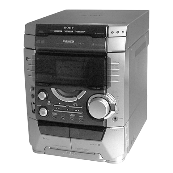
HCD-VX77/VX77J
SERVICE MANUAL
Ver 1.1 2001.08
HCD-VX77/VX77J is the tuner, deck, CD and
amplifier section in MHC-VX77/VX77J.
Amplifier section
The following measured at AC 120, 220, 240V
50/60 Hz
DIN power output (rated) 160 + 160 watts
(6 ohms at 1 kHz, DIN)
Continuous RMS power output (reference)
200 + 200 watts
(6 ohms at 1 kHz,
10% THD)
Inputs
MD/VIDEO (AUDIO) IN: voltage 450 mV/250 mV,
(phono jacks)
impedance 47 kilohms
MIC:
sensitivity 1 mV,
(phone jack)
impedance 10 kilohms
Outputs
VIDEO OUT:
max. output level 1 Vp-p,
(Phono jack)
unbalanced, Sync
negative, load impedance
75 ohms
S-VIDEO OUT:
Y: 1 Vp-p, unbalanced
(4 pin/mini-DIN jack)
Sync negative
C: 0.286 Vp-p
load impedence 75 ohms
PHONES:
accepts headphones of 8
(stereo mini jack)
ohms or more
accepts impedance of 6 to
FRONT SPEAKER:
16 ohms
SURROUND SPEAKER: accepts impedance of
16 ohms
Sony Corporation
9-929-223-12
Home Audio Company
2001H0200-1
Shinagawa Tec Service Manual Production Group
© 2001.8
Photo: HCD-VX77
Model Name Using Similar Mechanism
CD
CD Mechanism Type
SECTION
Base Unit Type
Optical Pick-up Type
Model Name Using Similar Mechanism
TAPE DECK
SECTION
Tape Transport Mechanism Type
SPECIFICATIONS
VIDEO CD/CD player section
System
Compact disc and digital
audio system
Laser
Semiconductor laser
(λ=780nm)
Emission duration:
continuous
Max. 44.6 µ W*
Laser output
*This output is the value
measured at a distance of
200 mm from the
objective lens surface on
the Optical Pick-up Block
with 7 mm aperture.
Frequency response
2 Hz – 20 kHz (±0.5 dB)
Wavelength
780 – 790 nm
Signal-to-noise ratio
More than 90 dB
Dynamic range
More than 90 dB
Video color system format
NTSC, PAL
CD OPTICAL DIGITAL OUT
(Square optical connector jack, rear panel)
Wavelength
660 nm
Output Level
–18 dBm
COMPACT DISC DECK RECEIVER
E Model
NEW
CDM58-K2BD37A
BU-K2BD37A
KSM-213DAP/Z-NP
NEW
TCM-230PWR11
Tape player section
Recording system
4-track 2-channel stereo
Frequency response
40 – 13,000 Hz (±3 dB),
using Sony TYPE I
cassette
Tuner section
FM stereo, FM/AM superheterodyne tuner
FM tuner section
Tuning range
87.5 – 108.0 MHz
Antenna
FM lead antenna
Antenna terminals
75 ohm unbalanced
Intermediate frequency
10.7 MHz
AM tuner section
Tuning range
Middle Eastern models:
531 – 1,602 kHz
(with the interval set at 9
kHz)
Other models:
531 – 1,602 kHz
(with the interval set at 9
kHz)
530 – 1,710 kHz
(with the interval set at 10
kHz)
Antenna
AM loop antenna
Antenna terminals
External antenna terminal
Intermediate frequency
450 kHz
— Continued on next page —
1
Advertisement
Table of Contents

Subscribe to Our Youtube Channel
Related Manuals for Sony HCD-VX77


Summary of Contents for Sony HCD-VX77
- Page 1 HCD-VX77/VX77J SERVICE MANUAL E Model Ver 1.1 2001.08 HCD-VX77/VX77J is the tuner, deck, CD and amplifier section in MHC-VX77/VX77J. Photo: HCD-VX77 Model Name Using Similar Mechanism CD Mechanism Type CDM58-K2BD37A SECTION Base Unit Type BU-K2BD37A Optical Pick-up Type KSM-213DAP/Z-NP Model Name Using Similar Mechanism...
-
Page 2: Table Of Contents
Ver 1.1 2001.08 TABLE OF CONTENTS General Power requirements Thailand models: 220 V AC, 50/60 Hz 1. SERVICE NOTE ······························································· 4 Other models: 120 V, 220 V or 230 - 240 V AC, 50/60 Hz 2. GENERAL ·········································································· 5 Adjustable with voltage selector 3. - Page 3 NOTES ON HANDLING THE OPTICAL PICK-UP BLOCK OR BASE UNIT The laser diode in the optical pick-up block may suffer electrostatic break-down because of the potential difference generated by the charged electrostatic load, etc. on clothing and the human body. During repair, pay attention to electrostatic break-down and also use the procedure in the printed matter which is included in the repair parts.
-
Page 4: Service Note
SECTION 1 SERVICE NOTE Note for installing the panel board 2 Panel board Hot melt Screw hole 1 Cut the eleven melted-connection points with a cutting plier. Attach the panel board with six screws (+BVTP 2.6 × 8 ) after the board is removed once. Do not tighten the screws excessively. -
Page 5: General
SECTION 2 GENERAL 2 3 4 qk qj Photo: HCD-VX77 DISC SKIP EX-CHANGE button ECHO LEVEL knob DISC 1 button and indicator EQ EDIT button DISC 2 button and indicator SPECTRUM button DISC 3 button and indicator DISPLAY button Z OPEN/CLOSE button... - Page 6 This section is extracted from instruction manual.
-
Page 7: Disassembly
SECTION 3 DISASSEMBY Note : Follow the disassembly procedure in the numerical order given. 9Two screws (+BVTP 3 × 10) Upper case (Top) 3-1. UPPER CASE (TOP) 5Two screws (Case) 7Two screws (+BVTP 3 × 10) Claw Side panel R Side panel L 6Screw (Case) 3Two screws... - Page 8 3-3. FRONT PANEL SECTION 0Two screws (+BVTP 3 × 10) qaTwo screws (+BVTP 2.6 × 8) 8Connector (CN201) CD mechanism deck (CDM58) 4Screw (+BVTP 3 × 10) Connector (CN601) 1Flat type wire (CN304) 5Screw (+BVTP 3 × 10) 2Connector (CN1) 9Connector (CN202) 3Connector (CN2) Front panel section...
- Page 9 3-5. PANEL BOARD 0Three claws 9Three screws (+BVTP 2.6 × 8) 7Knob(MIC) qaCD Switch board 6Spring 2Two screws qfPanel board (+BVTP 2.6 × 8) qdFive claws 3Two bosses & four pins 5FR knob qsCut the eleven melted-connection points with a cutting plier. 4Bracket (FR) Note: When attching the panel board, refer to "Service Note"...
- Page 10 3-7. MAIN BOARD AND AMP BOARD 4Three screws (+BVTP 3 × 8) 7Heat sink 6Two screws (+BVTP 3 × 8) 5Power AMP board Connector(CN502) 3Two screws (+BVTP 3 × 16) Connector (CN503) 2Main board 1Two screws (+BVTP 3 × 8) 3-8.
- Page 11 3-9. BASE UNIT 4Two insulators Base unit 1Flat type wire (CN101) 5Two insulators 2Four screws (+PTPWH 2.6) 3-10. DRIVER BOARD, MOTOR BOARD SENSOR BOARD AND VIDEO BOARD 9Screw (+PTPWH 2.6 × 8) 4Three screws (+BVTP 2.6 × 8) 6Motor board 7Flat type wire (CN721) 5Remove the two solderings of motor.
-
Page 12: Test Mode
SECTION 4 TEST MODE [MC Cold Reset] [Change-over of MW Tuner Step between 9 kHz and • The cold reset clears all data including preset data stored in the 10 kHz] RAM to initial conditions. Execute this mode when returning •... - Page 13 [MC Test Mode] • This mode is used to check operations of the respective sections of Amplifier, Tuner, CD and Tape. Procedure: Press the ?/1 button to turn on the set. Press the three buttons of x , ENTER and DISC 3 simultaneously.
- Page 14 [Aging Mode] This mode can be used for operation check of CD section and tape deck section. • If an error occurred: The aging operation stops and display status. • If no error occurs: The aging operation continues repeatedly. 1. Operating method of Aging Mode Turn on the main power and select “CD”...
- Page 15 2) Operation during aging mode In the aging mode, the program is executed in the following sequence. (1) The disc tray opens and closes. (2) The mechanism accesses DISC 2 and makes an attempt to read TOC. However, since there are no discs, a message “CD2 NO DISC”...
- Page 16 VIDEO CD COLOR-BARS MODE On this mode, the data of the color-bars signal as a picture signal and the 1kHz sine wave signal as a sound signal are output by the mechanism control microcomputer (IC502) for video CD signal check. When measurement of the voltage and waveform on the VIDEO board, perform it in this mode.
-
Page 17: Mechanical Adjustments
SECTION 5 SECTION 6 MECHANICAL ADJUSTMENTS ELECTRICAL ADJUSTMENTS Precaution DECK SECTION 0 dB=0.775 V 1. Clean the following parts with a denatured alcohol-moistened swab: 1. Demagnetize the record/playback head with a head record/playback heads pinch rollers demagnetizer. erase head rubber belts 2. - Page 18 DECK B 2. Turn the adjustment screw and check output peaks. If the peaks Tape Speed Adjustment do not match for L-CH and R-CH, turn the adjustment screw Note: Start the Tape Speed adjustment as below after setting to the test so that outputs match within 1dB of peak.
- Page 19 DECK B REC Bias Adjustment 4. Mode: Record Procedure: INTRODUCTION MD/VIDEO (AUDIO) IN When set to the test mode performed in Tape Speed Adjustment, 315 Hz, 50 mV (–23.8 dB) AF OSC when the tape is rewound after recording, the “REC memory mode” blank tape 600 Ω...
- Page 20 FM Tuned Level Adjustment CD SECTION FM RF SSG Note : 1. CD Block is basically designed to operate without adjustment. 75 Ω coaxial Therefore, check each item in order given. 2. Use YEDS-18 disc (3-702-101-01) unless otherwise indicated. 3. Use an oscilloscope with more than 10MΩ impedance. 4.
- Page 21 Note: Clear RF signal waveform means that the shape “◊” can be clearly distinguished at the center of the waveform. RF signal waveform VOLT/DIV : 200mV TIME/DIV : 500ns level : 1.45 ± 0.3Vp-p E-F Balance (1 Track jump) Check oscilloscope BD board TP (TEO)
- Page 22 Adjustment Location : [ BD BOARD ] — SIDE B — (RF) IC102 (VC) (AGCCON) (DGND) (TEO) (FEO) (AGND) (IOP) VIDEO SECTION Frequency adjustment frequency counter Connect the frequency counter to check point of the VIDEO VIDEO board board. (27 MHz) Adjust CT503 of the VIDEO board so that the frequency counter –...
-
Page 23: Diagrams
HCD-VX77/VX77J SECTION 7 DIAGRAMS 7-1. CIRCUIT BOARD LOCATION THIS NOTE IS COMMON FOR PRINTED WIRING BOARDS AND SCHEMATIC DIAGRAMS. (In addition to this, the necessary note is printed in each block.) MOTOR Board DRIVER Board Note on Schematic Diagram: Note on Printed Wiring Boards: •... - Page 24 HCD-VX77/VX77J Waveforms – CD SECTION – – VIDEO SECTION – – PANEL BOARD – – MAIN BOARD – IC101 t; IC502 qd IC509 ql IC401 qa IC601 oa T301 4 RFAC XOUT LRCK STOP MODE STOP MODE TAPE B REC MODE 4.6Vp-p...
-
Page 25: Block Diagrams - Tuner/Cd Section
HCD-VX77/VX77J 7-2. BLOCK DIAGRAMS AM/FM IF MPX TM601 LPF601 FE602 Q602 IC601 – TUNER/CD SECTION – CF601 CF602 RF IF BUFFER L-CH • RCH is omitted ANT IN IF OUT FM IF L OUT Q611 • Signal Path FM 75Ω... - Page 26 HCD-VX77/VX77J – VIDEO SECTION – D-RAM IC507 IC506 16 - 19 22 - 26 2 - 10 31 - 39 13 - 15 17 - 21 25 4 28 29 3 2 30 12 - 5 27 26 23 13 14 28 29...
- Page 27 HCD-VX77/VX77J – MAIN SECTION – J102 SURROUND SPEAKER R CH INPUT SELECT TONE/VOL CONT IC101 IC102 IC501 TM801 TUNER L-CH SECTION IN2A VOL OUT2 POWER (Page 25) Q504,505 Q861 Q821,822 SPEAKER RY801 Q824,825 VIDEO R CH LOUT MUTE MUTE MUTE...
-
Page 28: Printed Wiring Board - Bd Section
HCD-VX77/VX77J 7-3. PRINTED WIRING BOARD – BD SECTION – • See page 23 for Circuit Boards Location. -
Page 29: Schematic Diagram - Bd Section
HCD-VX77/VX77J 7-4. SCHEMATIC DIAGRAM – BD SECTION – • See page 24 for Waveforms. • See page 57 for IC Block Diagrams. • See page 48 for IC Pin Function. FUNCTION... -
Page 30: Printed Wiring Board - Video Section
HCD-VX77/VX77J 7-5. PRINTED WIRING BOARD – VIDEO SECTION – • See page 23 for Circuit Boards Location. • Semiconductor Location Ref. No. Location • Semiconductor Location D501 Ref. No. Location IC101 IC303 IC301 IC504 IC302 IC505 IC304 IC507 IC501 IC509... -
Page 31: Schematic Diagram - Video (1/3) Section
HCD-VX77/VX77J 7-6. SCHEMATIC DIAGRAM – VIDEO (1/3) SECTION – • See page 24 for Waveforms. • See page 60 for IC Block Diagrams. • See page 49 for IC Pin Function. FUNCTION... -
Page 32: Schematic Diagram - Video (2/3) Section
HCD-VX77/VX77J 7-7. SCHEMATIC DIAGRAM – VIDEO (2/3) SECTION – • See page 24 for Waveforms. • See page 49 for IC Pin Function. • See page 30 for Printed Wiring Board. FUNCTION... -
Page 33: Schematic Diagram - Video (3/3) Section
HCD-VX77/VX77J 7-8. SCHEMATIC DIAGRAM – VIDEO (3/3) SECTION – • See page 24 for Waveforms. • See page 49 for IC Pin Function. • See page 30 for Printed Wiring Board. -
Page 34: Printed Wiring Board - Main Section
HCD-VX77/VX77J 7-9. PRINTED WIRING BOARD – MAIN SECTION – • See page 23 for Circuit Boards Location. • Semiconductor Location Ref. No. Location (Page 30) (Page 44) D501 TO DRIVER BOARD TO VIDEO BOARD D502 D503 D504 D505 D506 D508... -
Page 35: Schematic Diagram - Main (1/3) Section
HCD-VX77/VX77J 7-10. SCHEMATIC DIAGRAM – MAIN (1/3) SECTION – • See page 59 for IC Block Diagrams. -
Page 36: Schematic Diagram - Main (2/3) Section
HCD-VX77/VX77J 7-11. SCHEMATIC DIAGRAM – MAIN (2/3) SECTION – • See page 24 for Waveforms. • See page 58 for IC Block Diagrams. • See page 54 for IC Pin Function. • See page 34 for Printed Wiring Board. FUNCTION... -
Page 37: Schematic Diagram - Main (3/3) Section
HCD-VX77/VX77J 7-12. SCHEMATIC DIAGRAM – MAIN (3/3) SECTION – • See page 34 for Printed Wiring Board. -
Page 38: Printed Wiring Board - Power Amp Section
HCD-VX77/VX77J 7-13. PRINTED WIRING BOARD – POWER AMP SECTION – • See page 23 for Circuit Boards Location. (Page 46) (Page 34) (Page 34) (Page 46) -
Page 39: Schematic Diagram - Power Amp Section
HCD-VX77/VX77J 7-14. SCHEMATIC DIAGRAM – POWER AMP SECTION –... -
Page 40: Printed Wiring Board - Panel Section
HCD-VX77/VX77J 7-15. PRINTED WIRING BOARD – PANEL SECTION – • See page 23 for Circuit Boards Location. • Semiconductor Location Ref. No. Location D601 D602 D603 D611 D612 D613 D614 D615 D617 D618 D630 D631 D632 IC601 IC602 IC603 IC721... -
Page 41: Schematic Diagram - Panel Section
HCD-VX77/VX77J 7-16. SCHEMATIC DIAGRAM – PANEL SECTION – • See page 24 for Waveforms. • See page 58 for IC Block Diagrams. • See page 56 for IC Pin Function. FUNCTION... -
Page 42: Printed Wiring Board - Leaf Sw Section
HCD-VX77/VX77J 7-17. PRINTED WIRING BOARD – LEAF SW SECTION – • See page 23 for Circuit Boards Location. • Semiconductor Location Ref. No. Location D1001 D1002 IC1001 IC1002 Q1001 (Page 34) (Page 34) (Page 34) -
Page 43: Schematic Diagram - Leaf Sw Section
HCD-VX77/VX77J 7-18. SCHEMATIC DIAGRAM – LEAF SW SECTION –... -
Page 44: Printed Wiring Board - Driver Section
HCD-VX77/VX77J 7-19. PRINTED WIRING BOARD – DRIVER SECTION – • See page 23 for Circuit Boards Location. • Semiconductor Location Ref. No. Location D701 IC701 IC711 (Page 34) -
Page 45: Schematic Diagram - Driver Section
HCD-VX77/VX77J 7-20. SCHEMATIC DIAGRAM – DRIVER SECTION – • See page 58 for IC Block Diagrams. -
Page 46: Printed Wiring Board - Trans Section
HCD-VX77/VX77J 7-21. PRINTED WIRING BOARD – TRANS SECTION – • See page 23 for Circuit Boards Location. (Page 38) (Page 38) -
Page 47: Schematic Diagram - Trans Section
HCD-VX77/VX77J 7-22. SCHEMATIC DIAGRAM – TRANS SECTION –... -
Page 48: Ic Pin Function
HCD-VX77/VX77J 7-23. IC PIN FUNCTIONS • IC101 DIGITAL SIGNAL PROCESSOR (CXD3008Q) (BD Board) Pin No. Pin Name Function Pin No. Pin Name Function DVDD0 — Digital power supply Tracking error signal input XRST System reset Center servo analog input RFDC... - Page 49 • IC502 MPEG DECODER, MECHANISM CONTROL (M30624MCA-A34FP) (VIDEO Board (1/3)) Pin No. Pin Name Function SENSE Internal state (SENSE) monitor input (IC101) SENSE CLK Serial data reading clock output (IC101) RESOLUTION Serial data output (IC101) CROMA LEVEL Lach output (IC101) DSP CLK Serial data clock output (IC101) TSENS...
- Page 50 Pin No. Pin Name Function BUS XWRL Not used LO. BOOST Not used AUDIO MUTE Audio mute output “L” : mute (Not used) LOAD OUT Not used LOAD IN Not used INSW Not used OUTSW Not used MODEL 1 L : System input (Fixed at “L”) MODEL 2 L : System input (Fixed at “L”) TBLL...
- Page 51 • IC505 CD DECODER, SYSTEM CONTROL (CL680T-D1) (VIDEO Board (2/3)) Pin No. Pin Name Function – Not used – Ground CD-BCK CD Decode bit clock CD-DATA CD Decode data CD-LRCK CD Decode Left or Right channel selection clock CD-C2PO CD Decode C2 error data –...
- Page 52 Pin No. Pin Name Function Address data from CL680 to Microcode ROM/DRAM – Ground Address data from CL680 to Microcode ROM/DRAM VDD3 – +3.3V Power supply Address data from CL680 to Microcode ROM/DRAM Address data from CL680 to Microcode ROM/DRAM Address data from CL680 to Microcode ROM/DRAM –...
- Page 53 Pin No. Pin Name Function PGIO0 Not used PGIO8 Not used PGIO2/VSYNC/CSYNC Vertical synchronized signal of video signal AVDD PLL – +3.3V Power supply – Not used – Not used – Not used AGND PLL – Ground – Ground – Not used PGIO3/HSYNC H.
- Page 54 • IC401 MASTER CONTROL (M30622MAA-A25FP) (MAIN BOARD) Pin No. Pin Name Description SURROUND 1 Surround control signal output SURROUND 2 Surround control signal output SURROUND 3 Surround control signal output 498-DATA Data signal output for IC101 (M61504FP) 498-CLK Clock signal output for IC101 (M61504FP) Not used.
- Page 55 Pin No. Pin Name Description Not used. Not used. Not used. Not used. Not used. Not used. A TRIG A deck trigger control signal output.H=ON, L-OFF B TRIG B deck trigger control signal output.H=ON, L-OFF CAPM-H/L Capstan motor High/Low speed control signal output. CAPM-CONT Capstan motor REV/FWD/STOP control signal output.H=REV, L=FWD/STOP Not used.
- Page 56 • IC601 DISPLAY CONTROL (TMP88CP77F-1A22) (PANEL BOARD) Pin No. Pin No. Pin Name Pin Name Description Description VOLUME A VOLUME A VOLUME A signal input. VOLUME A signal input. VOLUME B VOLUME B VOLUME B signal input. VOLUME B signal input. HEADPHONE HEADPHONE Head phone detect signal input.
-
Page 57: Ic Block Diagrams
7-24. IC BLOCK DIAGRAMS IC102 BA5982FM (BD BOARD) BIAS IN PreVcc OPIN1 + OPIN4 + OPIN1 – OPIN4 – OPOUT1 OPOUT4 OPIN2 + OPIN3 + OPIN2 – OPIN3 – OPOUT2 OPOUT3 STAND BY STAND BY STBY1 STBY2 CH1 2 3 PowVcc2 PowVcc1 VO2 (–) - Page 58 IC103 LA2615 (MAIN BOARD) IC602 BA3830F-E2 (PANEL BOARD) REFFERENCE RESET 18 RESET CURRENT REFFERENCE 17 f01 CURRENT ANALOG LEVEL ON/OFF SURROUND LINE 16 f02 VREF LINE 15 f03 13 f05 RESET 12 f06 BIAS 11 REC Bias LEVEL GND1 10 VCC IC701 BA6956AN (DRIVER BOARD) CONTROL LOGIC...
- Page 59 IC601 BA1450 (MAIN BOARD) AM IF VREG DECODER DRIVER COMP IC302 µPC1330HA (MAIN BOARD) INVERTER COMPARATER SW R1 SW P1 CONT SW P2 SW R2 IC651 LC72130 (MAIN BOARD) SWALLOW COUNTER 1/16.1/17 4bits POWER REFERENCE RESET DIVIDER SWALLOW COUNTER 1/16.1/17 4bits REFERENCE DIVIDER PHASE DETECTOR...
- Page 60 IC302 NJM2255M (VIDEO BOARD) IC303 NJM2209M (VIDEO BOARD) SATURATION +Ø ADJUST (COLOR BURST) HUE ADJUST SATURATION SECONDARY LOWER CLAMP ADJUST DIFFERENTIATION LIMITER SYNC –X (COLOR BURST) GAIN ADJ CHIP SWITCH CONTROL LOWER LIMITER IC304 BA7665FS (VIDEO BOARD) Mute MUTEA 16 VCC1 75Ω...
-
Page 61: Exploded Views
SECTION 8 EXPLODED VIEWS NOTE: • -XX, -X mean standardized parts, so they may • Abbreviation The components identified by mark 0 or have some differences from the original one. EA : Saudi Arabia model dotted line with mark 0 are critical for safety. •... -
Page 62: Panel Section
A-4428-457-A PANEL BOARD, COMPLETE A-4428-978-A CD SWITCH BOARD, COMPLETE (VX77:TH) (VX77:MY,SP,EA,HK,IA,E) A-4473-045-A CD SWITCH BOARD, COMPLETE (VX77J) A-4428-980-A PANEL BOARD, COMPLETE (VX77:TH) 4-962-708-81 EMBLEM (4-A), SONY A-4473-047-A PANEL BOARD, COMPLETE (VX77J) 4-225-033-01 FR KNOB 4-951-620-01 SCREW (2.6X8), +BVTP 4-224-578-11 KNOB (MIC) -
Page 63: Main Board Section
8-3. MAIN BOARD SECTION E,IA,VX77J not supplied IA,E,TH,VX77J EA,SP,MY not supplied SP,MY,EA,HK The components identified by mark 0 or dotted line with mark 0 are critical for safety. Replace only with part number specified. Ref. No. Part No. Description Remarks Ref. -
Page 64: Tape Mechanism Deck Section-1
Ver 1.1 2001.08 8-4. TAPE MECHANISM DECK SECTION-1 (TCM-230PWR11) Note: Two different types of tape mechanism are used depending on models. They maintain compatibility as an entire mechanism even though there are some different parts are used. HP101 HRPE101 Ref. No. Part No. -
Page 65: Tape Mechanism Deck Section-2
Ver 1.1 2001.08 8-5. TAPE MECHANISM DECK SECTION-2 (TCM-230PWR11) Ref. No. Part No. Description Remarks Ref. No. Part No. Description Remarks X-4952-881-1 CHASSIS ASSY, MAIN 4-228-450-01 SPRING (REVERSE SLIDER),TORSION 3-041-946-01 BELT (CAPSTAN B) 3-019-208-01 WASHER, STOPPER 4-227-239-01 BELT (CAPSTAN C) 3-027-453-01 SPRING (GROUND), TENSION 3-016-568-01 BRACKET (MOTOR) 3-030-823-01 SCREW (+BVTT) (2X3.5) -
Page 66: Cd Mechanism Deck Section (Cdm58-K2Bd37A)
Ver 1.1 2001.08 8-6. CD MECHANISM DECK SECTION (CDM58-K2BD37A) M721 not supplied BU-K2BD37 The components identified by mark 0 or dotted line with mark 0 are critical for safety. Replace only with part number specified. Ref. No. Part No. Description Remarks Ref. -
Page 67: Base Unit Section (Bu-K2Bd37A)
Ver 1.1 2001.08 8-7. BASE UNIT SECTION (BU-K2BD37A) The components identified by mark 0 or dotted line with mark 0 are critical for safety. Replace only with part number specified. Ref. No. Part No. Description Remark 0 301 8-820-116-01 OPTICAL PICK-UP KSM-213DAP 1-769-069-11 WIRE (FLAT TYPE) (16 CORE) A-4725-003-A BD BOARD, COMPLETE 4-951-620-01 SCREW (2.6X8), +BVTP... -
Page 68: Electrical Parts List
SECTION 9 ELECTRICAL PARTS LIST NOTE: Ref. No. • Due to standardization, replacements in the Part No. Description • COILS Remarks Ref. No. Part No. Description Remarks When indicating parts by reference number, uH: µH parts list may be different from the parts please include the board name. - Page 69 DRIVER HEAD (A) CD SWITCH Ref. No. Part No. Description Remarks Ref. No. Part No. Description Remarks R147 1-216-041-00 METAL CHIP 1/10W Q634 8-729-422-57 TRANSISTOR BN1A4M-TP R148 1-216-001-00 METAL CHIP 1/10W R149 1-216-003-11 RES-CHIP 1/10W Q635 8-729-422-57 TRANSISTOR BN1A4M-TP R150 1-216-073-00 METAL CHIP 1/10W R154...
- Page 70 HEAD (B) LEAF SW MAIN Ref. No. Part No. Description Remarks Ref. No. Part No. Description Remarks 1-676-221-11 HEAD (B) BOARD A-4473-339-A MAIN BOARD, COMPLETE (VX77J) ************ ************************** 1-564-722-11 PIN, CONNECTOR (SMALL TYPE) 6P 7-685-646-79 SCREW +BVTP TYPE2 N-S ************************************************************** <...
- Page 71 MAIN Ref. No. Part No. Description Remarks Ref. No. Part No. Description Remarks C199 1-163-038-91 CERAMIC CHIP 0.1uF C360 1-163-005-11 CERAMIC CHIP 470PF C201 1-104-665-11 ELECT 100uF 20.00% 10V C362 1-163-017-00 CERAMIC CHIP 0.0047uF 5% C202 1-126-925-11 ELECT 470uF 20.00% 10V C363 1-163-017-00 CERAMIC CHIP 0.0047uF 5%...
- Page 72 MAIN Ref. No. Part No. Description Remarks Ref. No. Part No. Description Remarks C632 1-126-933-11 ELECT 100uF 20.00% 16V * CN301 1-568-449-11 HOUSING, CONNECTOR (PC BOARD) 3P C633 1-163-031-11 CERAMIC CHIP 0.01uF * CN304 1-569-934-11 SOCKET, CONNECTOR 17P C634 1-163-016-00 CERAMIC CHIP 0.0039uF 10% CN401 1-793-766-11 CONNECTOR, BOARD TO BOARD 30P...
- Page 73 MAIN Ref. No. Part No. Description Remarks Ref. No. Part No. Description Remarks IC301 8-759-652-80 IC HA12227F JR602 1-216-295-91 SHORT IC302 8-759-143-54 IC uPC1330HA JR603 1-216-296-91 SHORT IC303 8-759-656-83 IC NJM4580MD-TE JR604 1-216-296-91 SHORT IC304 8-759-656-83 IC NJM4580MD-TE IC401 8-759-652-48 IC M30622MAA-A25FP JR605 1-216-296-91 SHORT JR606...
- Page 74 MAIN Ref. No. Part No. Description Remarks Ref. No. Part No. Description Remarks Q611 8-729-120-28 TRANSISTOR 2SC2412K-T-146-QR R165 1-216-073-00 METAL CHIP 1/10W Q612 8-729-120-28 TRANSISTOR 2SC2412K-T-146-QR R166 1-216-065-91 RES-CHIP 4.7K 1/10W Q821 8-729-120-28 TRANSISTOR 2SC1623-T1-L5L6 R171 1-216-073-00 METAL CHIP 1/10W Q822 8-729-120-28 TRANSISTOR 2SC1623-T1-L5L6...
- Page 75 MAIN Ref. No. Part No. Description Remarks Ref. No. Part No. Description Remarks R360 1-216-045-00 METAL CHIP 1/10W R497 1-216-073-00 METAL CHIP 1/10W (EA) R361 1-216-049-91 RES-CHIP 1/10W R497 1-216-053-00 METAL CHIP 1.5K 1/10W R363 1-216-049-91 RES-CHIP 1/10W (EXCEPT EA) R364 1-216-045-00 METAL CHIP 1/10W...
- Page 76 MAIN MOTOR PANEL Ref. No. Part No. Description Remarks Ref. No. Part No. Description Remarks R667 1-216-222-00 RES-CHIP 1/8W < TERMINAL > R668 1-216-049-91 RES-CHIP 1/10W R669 1-216-065-91 RES-CHIP 4.7K 1/10W TM601 1-694-555-11 TERMINAL BOARD (4P) (FM/AM) R804 1-216-089-91 RES-CHIP 1/10W TM801 1-694-635-11 TERMINAL BOARD (4P) (SPEAKER)
- Page 77 PANEL Ref. No. Part No. Description Remarks Ref. No. Part No. Description Remarks C651 1-164-159-21 CERAMIC 0.1uF C756 1-162-282-31 CERAMIC 100PF C652 1-126-960-11 ELECT 20.00% 50V C757 1-162-282-31 CERAMIC 100PF C653 1-126-960-11 ELECT 20.00% 50V C758 1-162-282-31 CERAMIC 100PF C654 1-164-159-21 CERAMIC 0.1uF C759...
- Page 78 PANEL Ref. No. Part No. Description Remarks Ref. No. Part No. Description Remarks < JACK > R639 1-249-441-11 CARBON 100K 1/4W J631 1-785-569-11 JACK (SMALL TYPE) (PHONE) R640 1-249-441-11 CARBON 100K 1/4W J721 1-785-569-11 JACK (SMALL TYPE) (MIC1) R641 1-249-441-11 CARBON 100K 1/4W J722...
- Page 79 PANEL POWER AMP Ref. No. Part No. Description Remarks Ref. No. Part No. Description Remarks R731 1-247-881-00 CARBON 120K 1/4W A-4428-344-A POWER AMP BOARD, COMPLETE (VX77:MY,SP,EA,HK,IA,E) R732 1-249-417-11 CARBON 1/4W F ************************************** R733 1-249-429-11 CARBON 1/4W R734 1-247-807-31 CARBON 1/4W A-4473-170-A POWER AMP BOARD, COMPLETE (VX77:TH) R735 1-247-885-00 CARBON...
- Page 80 POWER AMP SENSOR TRANS Ref. No. Part No. Description Remarks Ref. No. Part No. Description Remarks < IC > R944 1-247-791-91 CARBON 1/4W IC501 8-749-017-06 IC STK412-150 R980 1-249-429-11 CARBON 1/4W < TRANSISTOR > < THERMISTOR > Q501 8-729-140-84 TRANSISTOR 2SC1841TP-PAFAEA TH501 1-807-796-11 THERMISTOR...
- Page 81 TRANS VIDEO Ref. No. Part No. Description Remarks Ref. No. Part No. Description Remarks < TRANSFORMER > C547 1-126-193-11 ELECT C548 1-165-319-11 CERAMIC CHIP 0.1uF 0 T971 1-435-262-11 TRANSFORMER, POWER (VX77J) C549 1-165-319-11 CERAMIC CHIP 0.1uF 0 T971 1-435-325-11 POWER TRANSFORMER (VX77) C550 1-163-275-11 CERAMIC CHIP 0.001uF...
- Page 82 VIDEO Ref. No. Part No. Description Remarks Ref. No. Part No. Description Remarks JW413 1-216-295-91 SHORT R516 1-216-073-00 METAL CHIP 1/10W JW504 1-216-295-91 SHORT R517 1-216-073-00 METAL CHIP 1/10W JW505 1-216-295-91 SHORT R518 1-216-073-00 METAL CHIP 1/10W JW513 1-216-295-91 SHORT R519 1-216-025-91 RES-CHIP 1/10W...
- Page 83 HCD-VX77/VX77J Ver 1.1 2001.08 Ref. No. Part No. Description Remarks Ref. No. Part No. Description Remarks MISCELLANEOUS ************* 1-792-246-11 WIRE (FLAT TYPE) (23 CORE) 1-773-045-11 WIRE (FLAT TYPE) (17 CORE) 1-769-987-11 WIRE (FLAT TYPE) (13 CORE) 0 108 1-575-653-11 CORD, POWER (VX77:E,IA,VX77J)
- Page 84 HCD-VX77/VX77J REVISION HISTORY Clicking the version allows you to jump to the revised page. Also, clicking the version at the upper right on the revised page allows you to jump to the next revised page. Ver. Date Description of Revision 2001.08...
Need help?
Do you have a question about the HCD-VX77 and is the answer not in the manual?
Questions and answers