Table of Contents
Advertisement
SERVICE MANUAL
Ver 1.2 2001.09
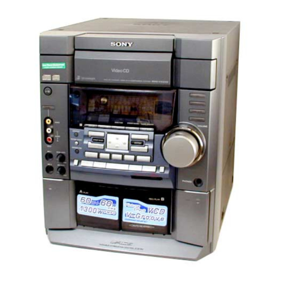
• HCD-VX222 is the tuner, deck, CD
and amplifier section in MHC-
VX222.
Amplifier section
The following measured at AC 120, 220, 240 V
50/60 Hz
DIN power output (rated) 50 + 50 watts
Continuous RMS power output (reference)
Inputs
MD/VIDEO (AUDIO) IN (phono jacks):
GAME (AUDIO) IN (phono jack):
MIC 1/2 (mini jack):
Sony Corporation
9-873-210-03
Home Audio Company
2001I0200-1
Shinagawa Tec Service Manual Production Group
© 2001. 9
HCD-VX222
CD
Section
Tape deck
Section
SPECIFICATIONS
(6 ohms at 1 kHz, DIN)
60 + 60 watts (6 ohms at
1 kHz, 10% THD)
voltage 450/250 mV,
impedance 47 kilohms
voltage 450 mV,
impedance 47 kilohms
sensitivity 1 mV,
impedance 10 kilohms
Model Name Using Similar Mechanism
CD Mechanism Type
Base Unit Name
Optical Pick-up Name
Model Name Using Similar Mechanism
Outputs
MD/VIDEO (AUDIO) OUT (phono jacks):
VIDEO OUT (phono jack):
S-VIDEO OUT (4-pin/mini-DIN jack):
PHONES (stereo mini jack):
SPEAKER:
MINI HI-FI COMPONENT SYSTEM
E Model
NEW
CDM58B-K6BD37A
BU-K6BD37A
KSM-213DCP/Z-NP
HCD-DX20/RG30
voltage 250 mV
impedance 1 kilohms
max. output level
1Vp-p, unbalanced, Sync
negative, load impedance
75 ohms
Y: 1Vp-p, unbalanced,
Sync negative,
C: 0.286Vp-p,
load impedance 75 ohms
accepts headphones of
8 ohms or more
accepts impedance of 6 to
16 ohms
— Continued on next page —
Advertisement
Table of Contents

Related Manuals for Sony HCD-VX222


Summary of Contents for Sony HCD-VX222
- Page 1 HCD-VX222 SERVICE MANUAL E Model Ver 1.2 2001.09 • HCD-VX222 is the tuner, deck, CD and amplifier section in MHC- VX222. Model Name Using Similar Mechanism CD Mechanism Type CDM58B-K6BD37A Section Base Unit Name BU-K6BD37A Optical Pick-up Name KSM-213DCP/Z-NP Tape deck...
- Page 2 MARK 0 ON THE SCHEMATIC DIAGRAMS AND IN THE PARTS LIST ARE CRITICAL TO SAFE OPERATION. REPLACE THESE Laser Semiconductor laser COMPONENTS WITH SONY PARTS WHOSE PART NUMBERS ( =780 nm) APPEAR AS SHOWN IN THIS MANUAL OR IN SUPPLEMENTS Emission duration: PUBLISHED BY SONY.
-
Page 3: Table Of Contents
HCD-VX222 TABLE OF CONTENTS 1. SERVICE NOTE .............. 4 2. GENERAL ................. 5 3. DISASSEMBY ..............7 4. TEST MODE ..............13 5. ELECTRICAL ADJUSTMENTS ......17 6. DIAGRAMS 6-1.Circuit Board Location ..........21 6-2.Block Diagrams –Tuner Section– ......... 22 Block Diagrams –Main Section–... -
Page 4: Service Note
HCD-VX222 SECTION 1 SERVICE NOTE REMOVING THE PANEL BOARD AND THE KEY BOARD * The panel board and the key board only are connected to the front panel by means of hot-melting the plastics. 5 Key board 3 Panel board... -
Page 5: General
HCD-VX222 SECTION 2 This section is extracted from GENERAL instruction manual. -
Page 6: Setting The Time
HCD-VX222 Setting the time Turn on the system. Press CLOCK/TIMER SET on the remote. Proceed to step 5 when “CLOCK” appears in the display. Press v or V repeatedly to select “SET CLOCK”. Press ENTER. Press repeatedly to set the hour. -
Page 7: Disassemby
HCD-VX222 SECTION 3 DISASSEMBLY Note : Disassemble the unit in the order as shown below. Case (Side-R, Side-L, Top) CD door Front panel section Tape mechanism deck Panel board Key board CD mechanism deck Video board, Base unit, BD board... - Page 8 HCD-VX222 3-2. CD DDOR CD door CD mechanism deck (CDM58B) 1 Turn the pulley to the direction of arrow. Front panel side pulley 2 Pull-out the disc tray. 3-3. CD MECHANISM DECK (CDM58B), FRONT PANEL SECTION, CHASSIS SECTION 4 Screw...
- Page 9 HCD-VX222 3-4. TAPE MECHANISM DECK 1 Six screws (+BVTP 2.6 × 8) 2 Tape mechanism deck 3-5. PANEL BOARD 6 Panel board 4 Connector (CN712) 2 Vol knob ring 5 Cut the seven melted-connection points with a cutting plier. 1 Volume knob Note: When attching the panel board, refer to "Service Note"...
- Page 10 HCD-VX222 3-6. KEY BOARD 2 Key board 1 Cut the six melted-connection points with a cutting plier. Note: When attching the Key board, refer to "Service Note" on page 4. 3-7. SUB TRANS BOARD, VIDEO OUT BOARD, BACK PANEL, POWER TRANSFORMER (TRANS BOARD)
- Page 11 HCD-VX222 3-8. MAIN BOARD, POWER AMP BOARD 7 Heat sink 6 Two screws (+BVTT 3 × 6) 4 Three screws (+BVTT 3 × 6) Main board 5 Power amp board 3 Two screws (+BVTP 3 × 16) 2 Main board 1 Two screws (+BVTT 3 ×...
- Page 12 HCD-VX222 3-10. DRIVER BOARD, MOTOR BOARD AND ADDRESS SENSOR BOARD q; Screw (+PTPWH 2.6 × 8) 4 Two screws (+BVTP 2.6 × 8) 8 Motor board 6 Wire (flat type)(CN721) 5 Remove the two solderings of motor. qs Screw (+BVTP 2.6 × 8)
-
Page 13: Test Mode
HCD-VX222 SECTION 4 TEST MODE [MC Cold Reset] [Change-over of AM Tuner Step between 9 kHz and • The cold reset clears all data including preset data stored in the 10 kHz] RAM to initial conditions. Execute this mode when returning •... - Page 14 HCD-VX222 [MC Test Mode] [Microprocessor version display] • This mode is used to check operations of the respective sections • If the following operation is performed during the POWER OFF of Amplifier, TUNER, CD and Tape. in the modes other than the POWER SAVE mode (i.e., while the...
- Page 15 HCD-VX222 [Aging Mode] This mode can be used for operation check of CD section and tape deck section. • If an error occurred: The aging operation stops and display status. • If no error occurs: The aging operation continues repeatedly.
- Page 16 HCD-VX222 2) Operation during aging mode [VIDEO CD Color-bars Mode] In the aging mode, the program is executed in the following On this mode, the data of the color-bars signal as a picture signal sequence. and the 1 kHz sine wave signal as a sound signal are output by the (1) The disc tray opens and closes.
-
Page 17: Electrical Adjustments
HCD-VX222 SECTION 5 ELECTRICAL ADJUSTMENTS FM Tuned Level Adjustment CD SECTION FM RF Signalgenerator Note : 1. CD Block is basically designed to operate without adjustment. 75 Ω coaxial Therefore, check each item in order given. 2. Use YEDS-18 disc (3-702-101-01) unless otherwise indicated. - Page 18 HCD-VX222 Note : Clear RF signal waveform means that the shape “ ◊ ” can be clearly Adjustment Location: distinguished at the center of the waveform. [BD BOARD] (Conductor Side) RF signal waveform VOLT/DIV : 200mV TIME/DIV : 500ns level : 1.45 ± 0.3Vp-p...
- Page 19 HCD-VX222 VIDEO SECTION Frequency Adjustment Connection: frequency counter VIDEO board (27 MHz) Procedure: 1. Connect the frequency counter to check point of the VIDEO board. 2. Turned power switch on. 3. Press the CD button to select the CD. 4. Adjust CT503 on the VIDEO board so that the frequency counter reading 27.0 MHz ±...
-
Page 20: Diagrams
HCD-VX222 SECTION 6 DIAGRAMS THIS NOTE IS COMMON FOR PRINTED WIRING BOARDS AND SCHEMATIC DIAGRAMS. (In addition to this, the necessary note is printed in each block.) Note on Schematic Diagram: Note on Printed Wiring Boards: • All capacitors are in µF unless otherwise noted. pF: µµF •... -
Page 21: 6-1.Circuit Board Location
HCD-VX222 6-1. CIRCUIT BOARD LOCATION • WAVEFORMS – BD BOARD – – MAIN BOARD – – PANEL BOARD – MOTOR board DRIVER board IC102 wf STOP MODE IC701 4 STOP MODE IC101 t; IC101 el ADDRESS SENSOR board (RFAC)(CD Play mode) -
Page 22: 6-2.Block Diagrams -Tuner Section
HCD-VX222 6-2. BLOCK DIAGRAMS AM/FM TUNER SECTION FRONT-END, IFAMP, MPX IC101 TM101 FE101 Q101 CF101 CF102 RF IF L-CH • RCH is omitted ANT IN IF OUT FM IF L OUT Q103 • Signal Path FM 75Ω OSC OUT MAIN... -
Page 23: Block Diagrams -Main Section
HCD-VX222 MAIN SECTION RV703 IC702 IC702 (1/2) (2/2) ECHO AMP LEVEL IC703 J703 MIC AMP MIC1 RV702 LPF IN LPF2 OUT ECHO LEVEL IC501 JK302 J702 TUNER L-CH SECTION TUNER L OUT L SPEAKER MIC2 (Page 22) POWER IMPEDANCE Q361,362... -
Page 24: Block Diagrams -Video Section
HCD-VX222 VIDEO SELECTOR MAIN VIDEO SW VIDEO SECTION SECTION IC704 (Page 23) TUNER XRST MAIN VIDEO SECTION SECTION (Page 22) (Page 23) VIDEO AMP TUNER IC304 CD DATA/CD BCK/CD LRCK/C2PO J705 SECTION (Page 22) VIDEO Y AMP MIX OUT1 IC303... -
Page 25: 6-3.Printed Wiring Board -Driver Section
HCD-VX222 6-3. PRINTED WIRING BOARD – DRIVER SECTION – • See page 21 for Circuit Boards Location. • Semiconductor Location C712 Ref. No. Location D701 IC701 IC711 (Page 28) • See page 50 for IC Block Diagrams. 6-4. SCHEMATIC DIAGRAM – DRIVER SECTION –... -
Page 26: 6-5.Printed Wiring Board -Bd Section
HCD-VX222 6-5. PRINTED WIRING BOARD – BD SECTION – • See page 21 for Circuit Boards Location. • Semiconductor Location Ref. No. Location IC101 IC102 IC103 IC104 Q101 VIDEO BOARD (Page 40) (KSM-213DCP) -
Page 27: 6-6.Schematic Diagram -Bd Section
HCD-VX222 6-6. SCHEMATIC DIAGRAM – BD SECTION – • See page 21 for Waveforms. • See page 48,49 for IC Block Diagrams. (KSM-213DCP) CN501 The components identified by mark 0 or dotted line with mark 0 are critical for safety. -
Page 28: 6-7.Printed Wiring Board -Main Section
HCD-VX222 6-7. PRINTED WIRING BOARD – MAIN SECTION – • See page 21 for Circuit Boards Location. DRIVER VIDEO BOARD MAIN BOARD BOARD (Page 25) (Page 40) • Semiconductor Location CLP2 JW232 JR633 R119 Ref. No. Location Ref. No. Location... -
Page 29: 6-8.Schematic Diagram -Main Section (1/5)
HCD-VX222 6-8. SCHEMATIC DIAGRAM – MAIN SECTION (1/5) – • See page 50 for IC Block Diagrams. -
Page 30: 6-9.Schematic Diagram -Main Section (2/5)
HCD-VX222 6-9. SCHEMATIC DIAGRAM – MAIN SECTION (2/5) – • See page 21 for Waveforms. • See page 49,50 for IC Block Diagrams. -
Page 31: Schematic Diagram -Main Section (3/5)
HCD-VX222 6-10. SCHEMATIC DIAGRAM – MAIN SECTION (3/5) –... -
Page 32: Schematic Diagram -Main Section (4/5)
HCD-VX222 6-11. SCHEMATIC DIAGRAM – MAIN SECTION (4/5) – • See page 21 for Waveforms. • See page 43 for IC Pin Function Description. -
Page 33: Schematic Diagram -Main Section (5/5)
HCD-VX222 6-12. SCHEMATIC DIAGRAM – MAIN SECTION (5/5) –... -
Page 34: Printed Wiring Board -Power Amp Section
HCD-VX222 6-13. PRINTED WIRING BOARD – POWER AMP SECTION – • See page 21 for Circuit Boards Location. POWER AMP BOARD (CHASSIS) • Semiconductor Location Ref. No. Location D501 D502 D541 D542 D543 D551 IC501 R519 Q501 MAIN BOARD Q503... -
Page 35: Schematic Diagram -Power Amp Section
HCD-VX222 6-14. SCHEMATIC DIAGRAM – POWER AMP SECTION –... -
Page 36: Printed Wiring Board -Panel Section
HCD-VX222 6-15. PRINTED WIRING BOARD – PANEL SECTION – • See page 21 for Circuit Boards Location. PANEL BOARD • Semiconductor Location Ref. No. Location TUNER/BAND D701 D702 61 60 IC701 D703 D704 DX20 R751 D705 C776 D706 JW714 D707... -
Page 37: Schematic Diagram -Panel Section
HCD-VX222 6-16. SCHEMATIC DIAGRAM – PANEL SECTION – • See page 21 for Waveforms. • See page 45 for IC Block Diagrams. -
Page 38: Printed Wiring Board -Trans Section
HCD-VX222 6-17. PRINTED WIRING BOARD – TRANS SECTION – • See page 21 for Circuit Boards Location. SUB TRANS BOARD • Semiconductor Location E,EA,IA,SP,TW Ref. No. Location D901 D902 D903 D904 D905 D911 AC IN D912 D913 IC901 Q901 Q911... -
Page 39: Schematic Diagram -Trans Section
HCD-VX222 6-18. SCHEMATIC DIAGRAM – TRANS SECTION –... -
Page 40: Printed Wiring Board -Video Cd Section
HCD-VX222 6-19. PRINTED WIRING BOARD – VIDEO CD SECTION – • See page 21 for Circuit Boards Location. • Semiconductor Location Ref. No. Location D501 PANEL BOARD (Page 36) IC101 IC301 IC302 IC303 IC304 IC501 IC502 IC504 IC505 IC506 IC507... -
Page 41: Schematic Diagram -Video Cd Section (1/2)
HCD-VX222 6-20. SCHEMATIC DIAGRAM – VIDEO CD SECTION (1/2) – • See page 21 for Waveforms. • See page 46 for IC Pin Function Description. • See page 51 for IC Block Diagrams. CN501 M30620MCA-B22FP BD BOARD CN301 CN101 (Page 27) -
Page 42: Schematic Diagram -Video Cd Section (2/2)
HCD-VX222 6-21. SCHEMATIC DIAGRAM – VIDEO CD SECTION (2/2) – • See page 21 for Waveforms. • See page 51 for IC Block Diagrams. (Page 41) C561 IC B/D IC506 MT23C020-H001S... -
Page 43: Ic Pin Function Description
HCD-VX222 6-22. IC PIN FUNCTION DESCRIPTION • MAIN BOARD (4/5) IC401 M30622MAA-A98FP (MASTER CONTROL) Pin No. Pin Name Description S-OUT Serial data output the display control. S-CLK Serial clock output from main controller. S-BSY Busy signal input from the display control. “L” : busy REMOTE IN Pemoto commander input. - Page 44 HCD-VX222 Pin No. Pin Name Description NO USE — Not used. CENT-MUTE — Not used. REAR-MUT — Not used. 494-DAT — Not used. 494-CLK — Not used. 494-LT — Not used. SUR1 Surround control signal output. SUR2 Surround control signal output.
- Page 45 HCD-VX222 • PANEL BOARD IC701 UPD780232GC-031-8BT (DISPLAY CONTROL) Pin No. Pin Name Description Power supply.(+5V) — Connected to ground. System clock output terminal.(5MHz) System clock input terminal.(5MHz) — Connected to ground. RESET Reset signal input from main controller. S-CLK Serial clock input from main controller.
- Page 46 HCD-VX222 VIDEO BOARD IC502 M30620MCA-B22FP (CD MECHANISM CONTROLLER) Pin No. Pin Name Description SENSE Internal status (SENSE) signal input from the CXD3008Q (IC101) SENSE CLK Sense serial data reading clock signal output to the CXD3008Q (IC101) RESOLUTION Y resolution output...
- Page 47 HCD-VX222 Pin No. Pin Name Description OUTSW Disc detection (load out) switch input terminal. Not used (fixed at “H”) MODEL1 Destination setting terminal (fixed at “L”) MODEL2 Destination setting terminal (fixed at “L”) TBLL — Not used (open) TBLR —...
-
Page 48: Ic Block Diagrams
HCD-VX222 6-23. IC BLOCK DIAGRAMS IC101 CXD3008Q (BD BOARD) 80 79 78 77 76 75 74 73 72 71 70 69 68 67 66 LRCK XRST DIGITAL DOUT MUTE DATA DATA ASYE XLAT XLAT INTERFACE CLOK CLOK INTERFACE SENS SENS... - Page 49 HCD-VX222 IC103 CXA2568M-T6 (BD BOARD) IC102 BA5982FM (BD BOARD) BIAS IN PreVcc APC PD AMP LC/PD OPIN1 + OPIN4 + LD_ON OPIN1 – OPIN4 – HOLD AGCVTH VREF OPOUT1 OPOUT4 APC LD AMP HOLD_SW OPIN2 + OPIN3 + AGCCONT (50%/30% OPIN2 –...
- Page 50 HCD-VX222 IC101 BA1450 (MAIN BOARD) AM IF VREG DECODER DRIVER COMP IC701 BA6956AN (DRIVER BOARD) IC201 TA8189N (MAIN BOARD) METAL TAPE A CH2/A CH2/B /TAPE B – – CONTROL LOGIC VREF1 IREF VREF2 – – CH1/A CH1/B METAL GND1...
- Page 51 HCD-VX222 IC303 NJM2209M (VIDEO BOARD) IC304 BA7665FS-E2 (VIDEO BOARD) MUTE VCC1 MUTEA 75Ω OUTA1 OUTA2 SECONDARY LOWER CLAMP DIFFERENTIATION LIMITER SYNC VCC2 GAIN ADJ CHIP SWITCH 75Ω MIXOUT1 CONTROL LOWER LIMITER MIXOUT2 N.C. 75Ω N.C. MUTEB OUTB CHROMA MUTE IC509...
-
Page 52: Exploded Views
HCD-VX222 SECTION 7 Ver 1.2 2001.09 EXPLODED VIEWS NOTE: The components identified by • Items marked “*” are not stocked since they are • Abbreviation mark 0 or dotted line with mark seldom required for routine service. Some delay : Saudi Arabia model 0 are critical for safety. -
Page 53: 7-2.Front Panel Section
HCD-VX222 Ver 1.2 2001.09 7-2. FRONT PANEL SECTION * For service only (Be sure to refer to "Service note" on page 4.) FLD1 not supplied not supplied Ref. No. Part No. Description Remark Ref. No. Part No. Description Remark 4-234-019-11 VOLUME KNOB… (BLACK) 4-224-562-01 BRACKET (HEART CAM L) 4-237-847-01 VOLUME KNOB…... -
Page 54: 7-3.Chassis Section
HCD-VX222 7-3. CHASSIS SECTION EA, SP, TW EA, SP, TW, E91 E, IA T911 EA, IA, TH not supplied Ref. No. Part No. Description Remark Ref. No. Part No. Description Remark 1-773-049-11 WIRE (FLAT TYPE) (17 CORE) 3-703-244-00 BUSHING (FBS001), CORD (EA,SP,TW,E91) -
Page 55: 7-4.Cd Mechanism Deck Section
HCD-VX222 7-4. CD MECHANISM DECK SECTION M721 supplied not supplied supplied Ref. No. Part No. Description Remarks Ref. No. Part No. Description Remarks 4-227-045-11 SPRING (INSULATOR), COIL 4-933-134-11 SCREW (+PTPWH M2.6X8) 4-221-679-01 CAM (RELAY) 4-985-672-01 SCREW (+PTPWH M2.6), FLOATING 4-231-452-01 TABLE (NEW) -
Page 56: Electrical Parts List
HCD-VX222 SECTION 8 ADDRESS SENOR ELECTRICAL PARTS LIST NOTE: Ref. No. Part No. Description Remarks Ref. No. Part No. Description Remarks • Due to standardization, replacements in the • COILS uH: µH parts list may be different from the parts... - Page 57 HCD-VX222 DRIVER Ref. No. Part No. Description Remarks Ref. No. Part No. Description Remarks R110 1-216-295-00 SHORT < CAPACITOR > R112 1-216-025-11 RES-CHIP 1/10W C702 1-126-964-51 ELECT 10uF R123 1-216-073-00 RES-CHIP 1/10W R124 1-216-097-11 RES-CHIP 100K 1/10W < CONNECTOR >...
- Page 58 HCD-VX222 MAIN Ref. No. Part No. Description Remarks Ref. No. Part No. Description Remarks R733 1-249-420-11 CARBON 1.8K 1/4W C106 1-126-933-11 ELECT 100uF R734 1-249-422-11 CARBON 2.7K 1/4W C107 1-162-970-11 CERAMIC CHIP 0.01uF R735 1-247-843-11 CARBON 3.3K 1/4W C108 1-126-964-11 ELECT...
- Page 59 HCD-VX222 MAIN Ref. No. Part No. Description Remarks Ref. No. Part No. Description Remarks C225 1-126-963-11 ELECT 4.7uF C333 1-130-475-00 MYLAR 0.0022uF 5% C226 1-162-977-11 CERAMIC CHIP 0.0018uF 10% C334 1-130-475-00 MYLAR 0.0022uF 5% C227 1-162-949-11 CERAMIC CHIP 47PF C337 1-130-491-00 MYLAR 0.047uF...
- Page 60 HCD-VX222 MAIN Ref. No. Part No. Description Remarks Ref. No. Part No. Description Remarks C671 1-126-916-11 ELECT 1000uF 6.3V D666 8-719-988-61 DIODE 1SS355TE-17 C672 1-162-953-11 CERAMIC CHIP 100PF D667 8-719-988-61 DIODE 1SS355TE-17 C673 1-162-953-11 CERAMIC CHIP 100PF D668 8-719-988-61 DIODE 1SS355TE-17...
- Page 61 HCD-VX222 MAIN Ref. No. Part No. Description Remarks Ref. No. Part No. Description Remarks JK301 1-770-613-11 JACK, PIN 4P (MD/VIDEO (AUDIO)) Q302 8-729-141-30 TRANSISTOR 2SC3623A-LK JK302 1-694-635-12 TERMINAL BOARD (4P) (SPEAKER) Q361 8-729-900-80 TRANSISTOR DTC114ES Q362 8-729-900-63 TRANSISTOR DTA124ES < JUMPER RESISTOR >...
- Page 62 HCD-VX222 MAIN Ref. No. Part No. Description Remarks Ref. No. Part No. Description Remarks R135 1-216-829-11 METAL CHIP 4.7K 1/16W R259 1-216-821-11 METAL CHIP 1/16W R136 1-216-827-11 METAL CHIP 3.3K 1/16W R260 1-216-816-11 METAL CHIP 1/16W R137 1-216-809-11 METAL CHIP...
- Page 63 HCD-VX222 MAIN Ref. No. Part No. Description Remarks Ref. No. Part No. Description Remarks R363 1-216-821-11 METAL CHIP 1/16W R644 1-216-851-11 METAL CHIP 330K 1/16W R364 1-216-821-11 METAL CHIP 1/16W R645 1-216-833-11 METAL CHIP 1/16W R365 1-216-841-11 METAL CHIP 1/16W...
- Page 64 HCD-VX222 PANEL MAIN MOTOR Ref. No. Part No. Description Remarks Ref. No. Part No. Description Remarks X602 1-781-107-21 VIBRATOR, SERAMIC (16MHz) C737 1-162-294-31 CERAMIC 0.001uF ***************************************************** C738 1-104-665-11 ELECT 100uF C739 1-104-665-11 ELECT 100uF 1-675-910-14 MOTOR BOARD C740 1-126-959-11 ELECT 0.47uF...
- Page 65 HCD-VX222 PANEL Ref. No. Part No. Description Remarks Ref. No. Part No. Description Remarks D716 8-719-084-40 DIODE SEL5955A-TP15 R761 1-249-429-11 CARBON 1/4W D717 8-719-084-40 DIODE SEL5955A-TP15 R762 1-247-807-31 CARBON 1/4W D718 8-719-084-40 DIODE SEL5955A-TP15 R763 1-249-429-11 CARBON 1/4W D719 8-719-084-40 DIODE SEL5955A-TP15...
- Page 66 HCD-VX222 POWER AMP SUB TRANS Ref. No. Part No. Description Remarks Ref. No. Part No. Description Remarks A-4476-990-A POWER AMP BOARD, COMPLETE (E,EA,IA,SP) Q581 8-729-140-84 TRANSISTOR 2SC1841-PAFAEA A-4725-699-A POWER AMP BOARD, COMPLETE (TW) A-4726-000-A POWER AMP BOARD, COMPLETE (TH) < RESISTOR >...
- Page 67 HCD-VX222 SUB TRANS TRANS VIDEO Ref. No. Part No. Description Remarks Ref. No. Part No. Description Remarks D904 8-719-200-82 DIODE 11ES2 < TRANSFORMER > D905 8-719-200-82 DIODE 11ES2 0 T911 1-437-221-11 TRANSFORMER, POWER < IC > ****************************************************** IC901 8-759-158-62 IC TA78057S...
- Page 68 HCD-VX222 VIDEO Ref. No. Part No. Description Remarks Ref. No. Part No. Description Remarks C545 1-165-319-11 CERAMIC CHIP 0.1uF JW304 1-216-295-00 SHORT C546 1-165-319-11 CERAMIC CHIP 0.1uF JW413 1-216-295-00 SHORT C547 1-126-193-11 ELECT JW504 1-216-295-00 SHORT C548 1-165-319-11 CERAMIC CHIP 0.1uF...
- Page 69 HCD-VX222 VIDEO VIDEO OUT Ref. No. Part No. Description Remarks Ref. No. Part No. Description Remarks R508 1-216-073-00 RES-CHIP 1/10W MISCELLANEOUS R516 1-216-073-00 RES-CHIP 1/10W ************* R517 1-216-073-00 RES-CHIP 1/10W R518 1-216-073-00 RES-CHIP 1/10W 1-769-986-11 WIRE (FLAT TYPE) (13 CORE)
- Page 70 HCD-VX222 REVISION HISTORY Clicking the version allows you to jump to the revised page. Also, clicking the version at the upper right on the revised page allows you to jump to the next revised page. Ver. Date Description of Revision 2001.09...
Need help?
Do you have a question about the HCD-VX222 and is the answer not in the manual?
Questions and answers