Table of Contents
Advertisement
Quick Links
HCD-V8900/V8900AV
SERVICE MANUAL
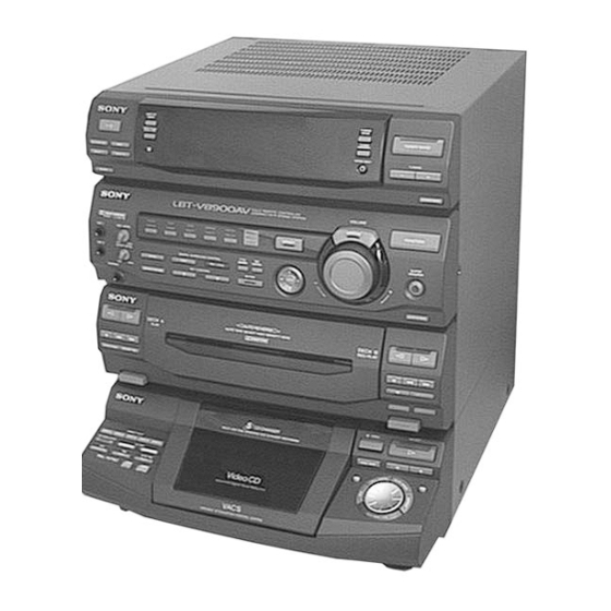
HCD-V8900/V8900AV is the tuner, deck, CD and
amplifier section in LBT-V8900AV/V8900S.
MICROFILM
Photo : HCD-V8900AV
Model Name Using Similar Mechanism
CD
CD Mechanism Type
SECTION
Base Unit Type
Optical Pick-up Type
TAPE
Model Name Using Similar Mechanism
DECK
Tape Transport Mechanism Type
SECTION
SPECIFICATIONS
COMPACT DISC DECK RECEIVER
– 1 –
E Model
HCD-V8900/V8900AV
Chinese Model
HCD-V8900AV
HCD-V4500
CDM37L-5BD21AL
BU-5BD21AL
KSS-213D/Q-NP
HCD-V4500
TCM-220WR2
— Continued on next page —
Advertisement
Table of Contents

Subscribe to Our Youtube Channel
Related Manuals for Sony HCD-V8900


Summary of Contents for Sony HCD-V8900
- Page 1 HCD-V8900/V8900AV SERVICE MANUAL E Model HCD-V8900/V8900AV Chinese Model HCD-V8900AV HCD-V8900/V8900AV is the tuner, deck, CD and amplifier section in LBT-V8900AV/V8900S. Photo : HCD-V8900AV Model Name Using Similar Mechanism HCD-V4500 CD Mechanism Type CDM37L-5BD21AL SECTION Base Unit Type BU-5BD21AL Optical Pick-up Type...
- Page 2 WITH MARK ! ON THE SCHEMATIC DIAGRAMS AND IN THE PARTS LIST ARE CRITICAL TO SAFE OPERATION. REPLACE THESE COMPONENTS WITH SONY PARTS WHOSE PART NUMBERS APPEAR AS SHOWN IN THIS MANUAL OR IN SUPPLEMENTS PUBLISHED BY SONY. – 2 –...
-
Page 3: Table Of Contents
MODEL IDENTIFICATION NOTES ON HANDLING THE OPTICAL PICK-UP BLOCK — BACK PANEL — • Abbreviation OR BASE UNIT SP : Singapore model MY : Malaysia model The laser diode in the optical pick-up block may suffer electrostatic IA : Indonesian model break-down because of the potential difference generated by the CH : Chinese model charged electrostatic load, etc. -
Page 4: General
SECTION 1 GENERAL Front Panel &¡ &º ^ª ^• ^¶ !º !¡ ^§ !™ ^¡^™^£^¢^∞ ^º !£ !¢ %ª !∞ %• %¢%∞%§%¶ !§ %£ !¶ %™ !• %¡ !ª %º @º $ª @¡ $• @™ @£ @¢ @∞ $¶ @§ @¶... - Page 5 This section is extracted from instruction manual. SECTION 2 DISASSEMBLY Note: Follow the disassembly procedure in the numerical order given. 2-1. FRONT PANEL 1 Three flat type wires (CN401, CN402, CN701) 3 Front panel 2 Four screws (BVTP3x8) – 5 –...
-
Page 6: Main Board
2-2. MAIN BOARD 5 Back panel 3 Six screws (BVTP3x8) 4 Power cord 2 Twelve screws 9 Connector (CN601) (BVTP3x8) 0 Connector 1 Flat type wire (CN851) (CN9001) !£ MAIN board 6 Connector (CN961) 8 Connector (CN830) !™ Connector (CN901) 7 Flat type wire (CN801) !¡... -
Page 7: Cassette Lid Assembly
2-4. CASSETTE LID ASSEMBLY 3 Two bracket 2 Two screws (BVTP2.6x8) 1 Two springs 4 Cassette lid assembly 2-5. CD LID ASSEMBLY 1 Four screws (BVTP2.6x8) 2 Connector (CN671) 4 CD lid assembly 3 Connector (CN661) – 7 –... -
Page 8: Cd Mechanism Deck
2-6. CD MECHANISM DECK 2-7. BASE UNIT 1 Five screws (BVTP3x8) 3 Flat type wire 2 CD mechanism deck 3 Base unit 2 Boss 1 Yoke bracket 2-8. DISC TABLE Note: When the disc table is installed, adjust the positions of roller cam and mark ”... -
Page 9: Service Mode
SECTION 3 SERVICE MODE MC Cold Reset • The cold reset clears all data including preset data stored in the RAM to initial conditions. Execute this mode when returning the set to the customer. Procedure: 1. Press three buttons SPECTRUM ANALYZER , ENTER , and DISC 1 simultaneously. 2. - Page 10 Aging Mode This mode can be used for operation check of CD section and tape deck section. • If an error occurred: The aging operation stops. • If no error occurs: The aging operation continues repeatedly. 1. Aging Mode in CD Section 1-1.
-
Page 11: Test Mode
SELF-DIAGNOSIS oscilloscope This model has the self-diagnosis function for the VIDEO and AUDIO decoder sections. Immediately after the power on, the self-diagnosis function searches VIDEO board TP709 (LED) each operation of IC’s around the mechanism control microcom- – puter (IC701). The results can be checked by connecting an oscilloscope to TP709 (LED) of the VIDEO board. -
Page 12: Mechanical Adjustments
SECTION 5 SECTION 6 MECHANICAL ADJUSTMENTS ELECTRICAL ADJUSTMENTS Precaution DECK SECTION 0 dB=0.775V 1. Clean the following parts with a denatured alcohol-moistened swab: 1. Demagnetize the record/playback head with a head damagnetizer. record/playback heads pinch rollers 2. Do not use a magnetized screwdriver for the adjustments. erase head rubber belts 3. - Page 13 2. Turn the adjustment screw and check output peaks. If the peaks Tape Speed Adjustment (Deck A) do not match for L-CH and R-CH, turn the adjustment screw so that outputs match within 1 dB of peak. Note: Set the test mode using the following method and begin tape speed adjustment.
- Page 14 Record Bias Adjustment (Deck B) Record Level Adjustment (Deck B) Procedure: Procedure: INTRODUCTION INTRODUCTION When set to the test mode performed in Tape Speed Adjust- When set to the test mode performed in Tape Speed Adjust- ment, when the tape is rewound after recording, the “REC memory ment, when the tape is rewound after recording, the “REC memory mode”...
- Page 15 CD SECTION Note : A clear RF signal waveform means that the shape “◊” can be clearly distinguished at the center of the waveform. NOTE : RF signal waveform 1. CD Block is basically designed to operate without adjustment. Therefore, check each item in order given. VOLT/DIV : 200mV 2.
- Page 16 VIDEO SECTION Video Frequency adjustment 1. Connect the frequency counter to check point of the VIDEO board. frequency counter VIDEO board TP410 (DCLK) – 2. Adjust CT401 of the VIDEO board so that the frequency counter read 13.5MHz ± 40Hz at STOP condition. Adjustment Location : [ BD BOARD ] —...
-
Page 17: Diagrams
HCD-V8900/V8900AV SECTION 7 DIAGRAMS 7-1. CIRCUIT BOARDS LOCATION 7-2. BLOCK DIAGRAMS – KEY CON SECTION – TRANS board VIDEO POWER board FM/AM TUNER PACK PANEL board MIC AMP ECHO AMP IC760 (2/2) IC760 (1/2) J761 MIC 1 RV760 MIC LEVEL... -
Page 18: Cd Section
HCD-V8900/V8900AV – CD SECTION – OPTICAL PICK-UP BLOCK (KSS-213D/Q-NP) DIGITAL SERVO RF AMP DIGITAL SIGNAL PROCESSOR LASER IC103 IC101 DIODE POWER APC LD LDON PRIORITY EMCODER 384FS DRIVE DOUT ADDRESS CLOCK Q101 DIGITAL GENERATOR EXCK GENERATOR SUBCODE SBSO PROCESSOR ASY0... -
Page 19: Video Section
HCD-V8900/V8900AV – VIDEO SECTION – 10BIT VIDEO D/A CONVERTER IC401 MPEG DECODER NOISE REDUCTION VIDEO AMP IC201 IC301 J9001 IC451 VIDEO OUT BUFFER IC501 (1/2) Y0-Y7 Y, C/Y, U, V • • SELECTOR VIDEO DEMPX, LEVEL MPEG MPEG MODULATOR &... -
Page 20: Deck Section
HCD-V8900/V8900AV – DECK SECTION – PB A/B S1004 S1008 B CrO A CrO CN403 R CH RV311 PLAYBACK IC611 A 120/70 LEVEL PB-A/B B 120/70 DECK A A IN PB OUT B IN PB L HP101 PB HEAD LM ON/... -
Page 21: Main Section
HCD-V8900/V8900AV – MAIN SECTION – VOLUME DOLBY PRO LOGIC IC604 DELAY IC601 CENTER REAR IC602 IC603 (Page 18) MUTE REAR L IN C-OUT REAR REAR Q602 DATA S-OUT S-OUT S-IN L-OUT L-IN FRONT LATCH FRONT L-MIX CENTER DATA J101 K CON... -
Page 22: Power Section
HCD-V8900/V8900AV – POWER SECTION – TM402 SURROUND POWER AMP SPEAKER IC601 REAR RY401 REAR –1 REAR REAR CENTER –2 CENTER CENTER CENTER RELAY DRIVE Q404 FAN MOTOR M901 DRIVER UNREG Q961, 962 MOTOR –12V OVER LOAD Q601,651 THERMAL TM401 Q670,671... - Page 23 HCD-V8900/V8900AV WAVEFORMS THIS NOTE IS COMMON FOR PRINTED WIRING BOARDS AND SCHEMATIC DIAGRAMS. – BD SECTION – – VIDEO SECTION – (In addition to this, the necessary note is printed in each block.) !∞ For schematic diagrams. 1.2Vp-p 1.3Vp-p Vp-p...
-
Page 24: Printed Wiring Board - Cd Section
HCD-V8900/V8900AV 7-3. PRINTED WIRING BOARD – CD SECTION – • See page 17 for Circuit Boards Location. (Page 36) • Semiconductor • Semiconductor Location (Side A) Location (Side B) Ref. No. Location Ref. No. Location IC101 IC101 IC103 Q101 – 31 –... -
Page 25: Schematic Diagram - Cd Section
HCD-V8900/V8900AV 7-4. SCHEMATIC DIAGRAM – CD SECTION – • See page 29 for Waveforms. • See page 96 for IC Pin Functions. (Page 39) – 33 – – 34 –... -
Page 26: Printed Wiring Board - Video Section
HCD-V8900/V8900AV 7-5. PRINTED WIRING BOARD – VIDEO SECTION – • See page 17 for Circuit Boards Location. (Page 48) (Page 32) (Page 38) • Semiconductor Location (Side A) Ref. No. Location IC101 IC102 • Semiconductor IC103 Location (Side B) IC201 IC271 Ref. -
Page 27: Schematic Diagram - Video (1/4) Section
HCD-V8900/V8900AV 7-6. SCHEMATIC DIAGRAM – VIDEO (1/4) SECTION – • See page 30 for Waveforms. • See page 90 for IC Block Diagrams. • See page 98 for IC Pin Functions. (Page 41) (Page 41) (Page 39) (Page 40) – 37 –... -
Page 28: Schematic Diagram - Video (2/4) Section
HCD-V8900/V8900AV 7-7. SCHEMATIC DIAGRAM – VIDEO (2/4) SECTION – • See page 30 for Waveforms. • See page 35 for Printed Wiring Board. • See page 102 for IC Pin Functions. (Page 37) (Page 37) (Page 43) (Page 39) (Page 43) –... -
Page 29: Schematic Diagram - Video (3/4) Section
HCD-V8900/V8900AV 7-8. SCHEMATIC DIAGRAM – VIDEO (3/4) SECTION – • See page 30 for Waveforms. • See page 35 for Printed Wiring Board. • See page 92 for IC Block Diagrams. • See page 104 for IC Pin Functions. (Page 38) -
Page 30: Schematic Diagram - Video (4/4) Section
HCD-V8900/V8900AV 7-9. SCHEMATIC DIAGRAM – VIDEO (4/4) SECTION – • See page 30 for Waveforms. • See page 35 for Printed Wiring Board. • See page 90 for IC Block Diagrams. (Page 41) (Page 40) (Page 52) (Page 56) (Page 40) –... -
Page 31: Printed Wiring Board - Key Control Section
HCD-V8900/V8900AV 7-10. PRINTED WIRING BOARD – KEY CONTROL SECTION – 7-11. SCHEMATIC DIAGRAM – KEY CONTROL SECTION – • See page 17 for Circuit Boards Location. • See page 95 for IC Block Diagrams. (Page 54) (Page 48) – 45 –... -
Page 32: Printed Wiring Board - Main Section
HCD-V8900/V8900AV 7-12. PRINTED WIRING BOARD – MAIN SECTION – • See page 17 for Circuit Boards Location. • Semiconductor Location Ref. No. Location D702 D772 D799 D901 D902 D903 (Page 79) (Page 35) D905 D906 D907 D908 D941 D942 D951... -
Page 33: Schematic Diagram - Main (1/5) Section
HCD-V8900/V8900AV 7-13. SCHEMATIC DIAGRAM – MAIN (1/5) SECTION – • See page 30 for Waveforms. • See page 93 for IC Block Diagrams. (Page 53) (Page 53) (Page 53) (Page 53) (Page 53) (Page 53) (Page 53) (Page 54) – 49 –... -
Page 34: Schematic Diagram - Main (2/5) Section
HCD-V8900/V8900AV 7-14. SCHEMATIC DIAGRAM – MAIN (2/5) SECTION – • See page 30 for Waveforms. • See page 47 for Printed Wiring Board. • See page 111 for IC Pin Functions. (Page 58) (Page 50) (Page 44) (Page 50) (Page 81) -
Page 35: Schematic Diagram - Main (3/5) Section
HCD-V8900/V8900AV 7-15. SCHEMATIC DIAGRAM – MAIN (3/5) SECTION – • See page 47 for Printed Wiring Board. • See page 94 for IC Block Diagrams. (Page 49) (Page 49) (Page 49) (Page 50) (Page 50) (Page 51) (Page 88) (Page 55) -
Page 36: Schematic Diagram - Main (4/5) Section
HCD-V8900/V8900AV 7-16. SCHEMATIC DIAGRAM – MAIN (4/5) SECTION – • See page 47 for Printed Wiring Board. • See page 94 for IC Block Diagrams. (Page 51) (Page 51) (Page 51) (Page 52) (Page 52) (Page 68) (Page 54) (Page 44) -
Page 37: Schematic Diagram - Main (5/5) Section
HCD-V8900/V8900AV 7-17. SCHEMATIC DIAGRAM – MAIN (5/5) SECTION – • See page 47 for Printed Wiring Board. • See page 94 for IC Block Diagrams. (Page 62) (Page 52) (Page 62) – 57 – – 58 –... -
Page 38: Printed Wiring Board - Deck Section
HCD-V8900/V8900AV 7-18. PRINTED WIRING BOARD – DECK SECTION – • See page 17 for Circuit Boards Location. (Page 47) (Page 47) • Semiconductor Location Ref. No. Location IC601 IC602 IC611 Q621 Q622 Q623 Q651 – 59 – – 60 –... -
Page 39: Schematic Diagram - Deck Section
HCD-V8900/V8900AV 7-19. SCHEMATIC DIAGRAM – DECK SECTION – • See page 94 for IC Block Diagrams. (Page 57) (Page 57) – 62 – – 61 –... -
Page 40: Printed Wiring Board - Power Section
HCD-V8900/V8900AV 7-20. PRINTED WIRING BOARD – POWER SECTION – • See page 17 for Circuit Boards Location. • Semiconductor Location Ref. No. Location D101 D102 D104 D105 D110 D111 D201 D251 D301 D302 D303 D321 G-10 D331 I-10 D332 I-10... -
Page 41: Schematic Diagram - Power Section
HCD-V8900/V8900AV 7-21. SCHEMATIC DIAGRAM – POWER SECTION – • See page 95 for IC Block Diagrams. (Page 85, 86) (Page (Page 88) (Page 88) – 65 – – 66 –... -
Page 42: Schematic Diagram - Panel Section
HCD-V8900/V8900AV 7-22. SCHEMATIC DIAGRAM – PANEL SECTION – • See page 29 for Waveforms. • See page 110 for IC Pin Functions. (Page 76) (Page 73) (Page 75) (Page 56) (Page 76) (Page 74) – 67 – – 68 –... -
Page 43: Printed Wiring Board - Panel Section
HCD-V8900/V8900AV 7-23. PRINTED WIRING BOARD – PANEL SECTION – • Semiconductor • See page 17 for Circuit Boards Location. Location Ref. No. Location D601 D602 D-10 D603 D604 D605 C-10 D606 D607 D611 D612 D613 D614 D615 D616 D617 D618... -
Page 44: Printed Wiring Board - Tc/Cd Panel-1 Section
HCD-V8900/V8900AV 7-24. PRINTED WIRING BOARD – TC/CD PANEL-1 SECTION – • See page 17 for Circuit Boards Location. (Page 69) (Page 70) – 71 – – 72 –... -
Page 45: Schematic Diagram - Tc/Cd Panel-1 Section
HCD-V8900/V8900AV 7-25 SCHEMATIC DIAGRAM – TC/CD PANEL-1 SECTION – (Page 67) (Page 67) – 73 – – 74 –... -
Page 46: Schematic Diagram - Hp/Mic Section
HCD-V8900/V8900AV 7-26. SCHEMATIC DIAGRAM – HP/MIC SECTION – • See page 95 for IC Block Diagrams. (Page 68) (Page 68) (Page 68) – 75 – – 76 –... -
Page 47: Printed Wiring Board - Hp/Mic Section
HCD-V8900/V8900AV 7-27. PRINTED WIRING BOARD – HP/MIC SECTION – • See page 17 for Circuit Boards Location. (Page 70) (Page 69) (Page 70) – 77 – – 78 –... -
Page 48: Printed Wiring Board - Cd Motor Section
HCD-V8900/V8900AV 7-28. PRINTED WIRING BOARD – CD MOTOR SECTION – • See page 17 for Circuit Boards Location. (Page 48) – 79 – – 80 –... -
Page 49: Schematic Diagram - Cd Motor Section
HCD-V8900/V8900AV 7-29. SCHEMATIC DIAGRAM – CD MOTOR SECTION – • See page 95 for IC Block Diagrams. (Page 52) – 81 – – 82 –... -
Page 50: Printed Wiring Board - Trans Section
HCD-V8900/V8900AV 7-30. PRINTED WIRING BOARD – TRANS SECTION – • See page 17 for Circuit Boards Location. (Page 64) (Page 64) – 83 – – 84 –... -
Page 51: Schematic Diagram - Trans Section
HCD-V8900/V8900AV 7-31. SCHEMATIC DIAGRAM – TRANS SECTION – (Page 66) (Page 66) – 85 – – 86 –... -
Page 52: Printed Wiring Board - Surround Section
HCD-V8900/V8900AV 7-32. PRINTED WIRING BOARD – SURROUND SECTION – 7-33. SCHEMATIC DIAGRAM – SURROUND SECTION – • See page 17 for Circuit Boards Location. (Page 53) (Page 65) (Page 66) (Page 48) (Page 63) (Page 64) • Semiconductor Location Ref. No. -
Page 53: Ic Block Diagrams
7-34. IC BLOCK DIAGRAMS • BD section IC101 CXD2545Q 67 62 63 64 20 19 32K RAM CLOCK GENERATOR C16M 43 PSSL DIGITAL ADDRESS PRIORITY VCO1 SERIAL GENERATOR ENCODER VCO0 PARALLEL DEMODULATOR VARI-PITCH 61-46 DA01-16 DOUBLE SPEED PROCESSOR FILI FILO 79 MUTE SYNC CLTV... - Page 54 • Video section IC101 CXD8567AM INIT D Vdd 2 SYSM L1 (+) A Vdd L SHIFT L2 (+) LATCH A Vss L 256FSO X Vss TEST1 512IN D Vss X OUT MCKSEL X Vdd XBCK A Vss R DATA R2 (+) LRCK A Vdd R MUTE L...
- Page 55 IC271 BU6257AFV 16 15 14 13 12 CHARACTER HORIZONTAL WRITE SIZE ADDRESS ADDRESS REGISTER REGISTER COUNTER CHARACTER DATA HORIZONTAL HORIZONTAL HORIZONTAL 3 BIT × 288 WORD SIZE POSITION ADDRESS COUNTER COUNTER COUNTER COLOR DATA 3 BIT × 288 WORD VERTICAL CHARACTER DATA 8 BIT ×...
- Page 56 IC501 SN74HC245ANS IC401 CXD1913Q 50 49 48 46 45 44 43 42 41 40 37-39 36 35 34 33 XTEST4 BURST FLAG CSYNC SYNC Slope SYNC Gen. Gen. XRST Sub Carrier Timing Controller TEST MODE Gen. SYSCLK PDCLK SIO and I O-Bus Closed Caption Encoder VSYNC...
- Page 57 • Main section IC102 MC14052BCP IC103, 1702 MC14053BCP B.COM OPEN A.COM C.COM OPEN OPEN IC601 LA2786 BPF1 NOISE NOISE FILTER BPF2 NOISE GENERATOR DATA BALANCE ENABLE VREF CONTROL V REF OSC1 DIVIDER CONTROL S-CH DC OUT C-CH DC OUT L-CH DC OUT R-CH DC OUT VREF L-IN...
- Page 58 IC604 TC9210P IC901 LA5617 CURRENT CURRENT START ON/OFF ON/OFF LIMITER LIMITER CIRCUIT L-CH R-CH DATA DATA VREF L-CH R-CH VMUTE LATCH LATCH CIRCUIT CIRCUIT OVER HEAT A-GND A-GND PROTECT VREF ERROR VREF ~ _ 1.8V SHIFT RESISTER ERROR (13bit) LEVEL LEVEL SHIFT SHIFT...
- Page 59 • HP/MIC section • Power section IC761 M65850P IC301 uPC1237HA OVER LOAD DET MUTE OSCILLATOR OFFSET DET LPF2 1/2 VCC CLOCK LATCH/ AUTORESET AUTO MAIN 20KBIT RESET RESET CONTROL SRAM AC OFF LPF1 • CD motor section IC201 TA8409S VREF BLOCK STANDBY BLOCK...
-
Page 60: Ic Pin Functions
7-35. IC PIN FUNCTIONS • IC101 DIGITAL SIGNAL PROCESSOR (CXD2545Q)/BD board Function Pin No. Pin Name Sled drive output (Not used) SRON Sled drive output SRDR SFON Sled drive output (Not used) Tracking drive output TFDR Tracking drive output (Not used) TRON Tracking drive output TRDR... - Page 61 Pin No. Function Pin Name DA 11 output when PSSL=1. GTOP output when PSSL=0 (Not used) GTOP DA 10 output when PSSL=1. XUGF output when PSSL=0 (Not used) XUGF XPLCK DA 09 output when PSSL=1. XPLCK output when PSSL=0 DA 08 output when PSSL=1. GFS output when PSSL=0 DA 07 output when PSSL=1.
- Page 62 • IC201 MPEG DECODER (CXD1856AQ)/VIDEO board Pin No. Function Pin Name – Ground Video decoder master clock pin. Input the XTL0I clock or connect an oscillator between XTL0O XTL0I and XTL0O. The recommended frequencies are 27MHz, 28.6363MHz (NTSC XTL0I 8fsc), and 35.4686 MHz (PAL 8fsc). –...
- Page 63 Pin Name Function Pin No. Data input/output signal pin. Connect to the DRAM data pin so that the lower and upper bytes of the data correspond to the CAS0 to CAS3 controls. MD10 – +5V power supply – Ground MD11 MD12 Data input/output signal pin.
- Page 64 Pin Name Pin No. Function B/Cb0 B/Cb1 B/Cb2 Output pin of the B or Cb signal of the image data. MSB is B/Cb7. Synchronizes with B/Cb3 DCLK. (Not used) B/Cb4 B/Cb5 B/Cb6 B/Cb7 Dot clock (DCLK) signal pin. The DCLK frequency is normally 13.5MHz. The DCLK can be input from this pin or can be made by frequency-dividing (1/integer) the clock input DCLK from XTL0I.
- Page 65 Pin No. Pin Name Function Serial data input (CXD2545Q) DATI Bit clock input (CXD2545Q) BCKI Digital input signal (Not used) DOIN Register access chip select signal pin. XHCS Data acknowledge/wait signal pin for DMA transmission, register access, transparent XHDT memory access. Register access control signal pin.
- Page 66 • IC301 NOISE REDUCTION (CXD1854Q)/VIDEO board Pin No. Pin Name Function – Ground [MSB] B input 0–7 (Connect to ground) [LSB] – Ground Y/GI7 [MSB] Y/GI6 Y/GI5 Y/GI4 G (Y) input 0–7 Y/GI3 Y/GI2 Y/GI1 Y/GI0 [LSB] – Ground C/RI7 [MSB] C/RI6 C/RI5...
- Page 67 Pin No. Pin Name Function [MSB] C/RO0 C/RO1 C/RO2 C/RO3 R (Cb/Cr) output 0–7 C/RO4 C/RO5 C/RO6 C/RO7 [LSB] Power supply (+5V) – Y/GO7 [MSB] Y/GO6 Y/GO5 Y/GO4 G (Y) output 0–7 Y/GO3 Y/GO2 Y/GO1 Y/GO0 [LSB] Power supply (+5V) –...
- Page 68 • IC401 10 BIT VIDEO D/A CONVERTER (CXD1913Q)/VIDEO board Pin No. Pin Name Function 8-bit pixel data input pins (PD0 to 7). When control register bit “PIF MODE”=“0”, serve as input pins for multiplexed Y, Cb, Cr signals. When control register bit “PIF MODE”=“1”, serve as input pins for Y signal –...
- Page 69 Digital ground The functions of this pin are selected by Pin 64 XIICEN. When the XIICEN pin is “H”, sets into the SONY SIO mode, and becomes the SI serial data input pin. When the XIICEN pin is “L”, sets into the I...
- Page 70 H.sync signal output The functions of this pin are selected by Pin 64 XIICEN. When the XIICEN pin is “H”, sets into the SONY SIO mode, and becomes the S0 serial- out output pin. When the XIICEN pin is “L”, this pin is not used and sets into high impedance (Not used) Field ID output.
- Page 71 • IC701 MECHANISM CONTROL (HD6433032SK12F)/VIDEO board Pin No. Function Pin Name Input/output terminal exchanging data bus 0 with IIC interface (IC901) CMD0 Input/output terminal exchanging data bus 1 with IIC interface (IC901) CMD1 Input/output terminal exchanging data bus 2 with IIC interface (IC901) CMD2 Input/output terminal exchanging data bus 3 with IIC interface (IC901) CMD3...
- Page 72 Pin No. Pin Name Function A/D converter (Pin62-29) power supply (Connected to +5V) AVCC – CHECK-LED Check LED control (Error : flashing) (Not used) XHIRQ Interruption request input from MPEG decoder Subcode sync input (CXD2545Q) SCOR MREQ Inputs command request from IIC interface (IC901) Serial data output DATA AMUTE...
- Page 73 • IC901 IIC INTERFACE (uPD780016YGF-020-3BA)/VIDEO board Pin No. Pin Name Function P80 to P87 Connected to ground 1 to 8 Connected to ground TEST – X’ tall (5MHz) X’ tall (5MHz) Power supply +5V – Not used – Connected to +5V –...
- Page 74 • IC601 DISPLAY CONTROL (TMP87CM75F-6565)/PANEL board Pin Name Function Pin No. SEG35 FL segment signal output VLOAD – Power supply (–25V) for FL segment signal output 3 to 10 LED1 to LED8 LED driver output – Ground X-OUT X’tall (8MHz) X-IN RESET Reset signal input from main controller...
- Page 75 • IC701 MASTER CONTROL (uPD780018YGF-023-3BA)/MAIN board Pin Name Function Pin No. TA-MUTE Line mute signal output DBFB-H/L DBFB H/L select signal output 427-LT Latch signal output for IC201 (62427) KCON-LT Latch signal output for key control (IC1401) KCON-ON Key control ON/OFF signal output F-RELAY Front speaker relay control output (Not used) R-RELAY...
- Page 76 Pin No. Pin Name Function MSM-LT MSM-NAR Not used MSM-CH INPUT-CHANGE Input sensitivity switching output IIC-DATA Data output for IC601/PANEL board, IC901/VIDEO board. IIC-CLK Clock output for IC601/PANEL board, IC901/VIDEO board. XRST CD reset signal output CD latch signal output (Not used) FOUCUS-SW Not used TBL-L...
-
Page 77: Exploded Views
SECTION 8 EXPLODED VIEWS NOTE: The components identified by • Abbreviation • Items marked “*” are not stocked since they are mark ! or dotted line with mark : Singapole model seldom required for routine service. Some delay ! are critical for safety. : Malaysia model should be anticipated when ordering these items. -
Page 78: Front Panel Section-1
8-2. FRONT PANEL SECTION-1 TCM-220WR2 Supplied with S711 Ref. No. Part No. Description Remark Ref. No. Part No. Description Remark 4-987-995-01 SPRING (CD EJECT), COMPRESSION * 67 1-664-013-11 TC-B SW BOARD 4-987-001-11 BUTTON (EJECT CD) * 68 1-664-020-11 CD-B1 SW BOARD * 53 1-664-019-11 CD-A SW BOARD X-4949-279-1 BUTTON (CD STOP) ASSY... -
Page 79: Front Panel Section-2
4-988-219-01 BUTTON (DOLBY) * 106 4-986-870-01 HOLDER, FL TUBE * 119 A-4407-938-A PANEL BOARD, COMPLETE 4-986-997-41 BUTTON (DECK.A) 4-963-404-21 EMBLEM (5-A), SONY * 119 A-4414-951-A PANEL BOARD, COMPLETE (V8900) 4-973-644-71 KNOB (MIC) 1-773-051-11 WIRE (FLAT TYPE)(17 CORE) 4-948-236-21 CUSHION (107) 4-951-620-01 SCREW (2.6X8), +BVTP... -
Page 80: Chassis Section
8-4. CHASSIS SECTION not supplied (IA, CH,TH) CNP901 (IA) T501 not supplied CNP901 not supplied (SP, MY) not supplied CDM37L-5BD21AL not supplied The components identified by mark ! or dotted line with mark ! are critical for safety. not supplied Replace only with part number specified. -
Page 81: Tc Mechanism Section-1 (Tcm-220Wr2)
8-5. TC MECHANISM SECTION-1 (TCM-220WR2) not supplied Ref. No. Part No. Description Remark Ref. No. Part No. Description Remark X-4947-943-1 HOLDER (L) ASSY, CASSETTE * 206 4-980-439-01 FULCLUM, HOLDER X-4947-944-1 HOLDER (R) ASSY, CASSETTE 3-354-957-01 JOINT (LOCK LEVER) 4-959-231-11 SPRING (L), TORSION 3-354-953-01 LEVER (LOCK LEVER L) 4-959-232-11 SPRING (R), TORSION 3-354-954-01 LEVER (LOCK LEVER R) -
Page 82: Tc Mechanism Section-2 (Tcm-220Wr2)
8-6. TC MECHANISM SECTION-2 (TCM-220WR2) (including p A) not supplied HP101 (includeing r A) not supplied not supplied HRPE101 (including p B) not supplied not suppl ied not supplied not supplied Ref. No. Part No. Description Remark Ref. No. Part No. Description Remark 3-908-560-01 SPRING, AZIMUTH ADJUSTMENT... -
Page 83: Tc Mechanism Section-3 (Tcm-220Wr2)
8-7. TC MECHANISM SECTION-3 (TCM-220WR2) pA: MOTOR board (Suppplied with AUDIO board) not supplied Ref. No. Part No. Description Remark Ref. No. Part No. Description Remark 3-908-597-01 CAM (A) 3-908-600-01 LEVER (REV-B) 3-908-608-11 SCREW, STEP X-3372-930-1 ARM (A) ASSY, FR * 316 1-650-669-11 LEAF SWITCH BOARD X-3370-169-1 FLYWHEEL (AR) ASSY... -
Page 84: Cd Mechanism Section (Cdm37L-5Bd21L)
8-8. CD MECHANISM SECTION (CDM37L-5BD21AL) not supplied M201 supplied Ref. No. Part No. Description Remark Ref. No. Part No. Description Remark 4-987-976-01 SCREW, STEP 4-978-426-01 INDICATOR (NO.) 4-944-490-01 BELT (TIMING) A-4660-978-A GEAR (PULLEY) ASSY * 366 1-659-059-13 LED BOARD 4-978-421-01 GEAR (MID) * 367 1-659-058-13 TABLE SENSOR BOARD 4-978-425-01 ROLLER (CAM) -
Page 85: Base Unit Section (Bu-5Bd21Al)
8-9. BASE UNIT SECTION (BU-5BD21AL) M101 M102 The components identified by mark ! or dotted line with mark ! are critical for safety. Replace only with part number specified. Ref. No. Part No. Description Remark Ref. No. Part No. Description Remark ! 401 8-820-020-02 OPTICAL PICK-UP KSS-213D/Q-NP... -
Page 86: Electrical Parts List
SECTION 9 AUDIO ELECTRICAL PARTS LIST Note: • Due to standardization, replacements in the parts list • SEMICONDUCTORS may be different from the parts specified in the In each case, u: µ , for example: diagrams or the components used on the set. uA...: µ... - Page 87 AUDIO CD-A SW Ref. No. Part No. Description Remark Ref. No. Part No. Description Remark R625 1-249-429-11 CARBON 1/4W < IC > R651 1-247-856-00 CARBON 1/4W R652 1-247-856-00 CARBON 1/4W IC101 8-752-369-78 IC CXD2545Q R653 1-249-441-11 CARBON 100K 1/4W IC102 8-759-176-09 IC BA6392FP IC103 8-752-072-45 IC CXA1821M-T6...
- Page 88 CD-A SW CD-B1 SW CD-B2 SW CD-LED CD MOTOR Ref. No. Part No. Description Remark Ref. No. Part No. Description Remark D642 8-719-058-04 DIODE SEL5223S-TP15 (VCD) S677 1-554-303-21 SWITCH, TACTILE (p) D643 8-719-058-04 DIODE SEL5223S-TP15 (PBC) S678 1-554-303-21 SWITCH, TACTILE (P) D644 8-719-058-04 DIODE SEL5223S-TP15 (AUTO PBC) S679...
- Page 89 DOOR SW HP/MIC CD MOTOR Ref. No. Part No. Description Remark Ref. No. Part No. Description Remark < COIL > C786 1-162-294-31 CERAMIC 0.001uF C787 1-124-250-11 ELECT 0.15uF L201 1-408-117-00 INDUCTOR 10uH C788 1-126-960-11 ELECT C789 1-161-494-00 CERAMIC 0.022uF < RESISTOR > C790 1-104-664-11 ELECT 47uF...
- Page 90 HP/MIC KEYCON LEAF SWITCH Ref. No. Part No. Description Remark Ref. No. Part No. Description Remark < VARIABLE RESISTOR > R1422 1-249-429-11 CARBON 1/4W R1431 1-247-903-00 CARBON 1/4W RV760 1-225-366-11 RES, VAR, CARBON 50K (MIC LEVEL) R1435 1-247-807-31 CARBON 1/4W RV761 1-225-366-11 RES, VAR, CARBON 50K (ECHO LEVEL) R1436...
- Page 91 MAIN Ref. No. Part No. Description Remark Ref. No. Part No. Description Remark < RESISTOR > C234 1-126-925-11 ELECT 470uF C235 1-164-159-21 CERAMIC 0.1uF R201 1-247-863-91 CARBON 1/4W R202 1-249-411-11 CARBON 1/4W C237 1-126-964-11 ELECT 10uF R203 1-249-437-11 CARBON 1/4W C238 1-162-286-21 CERAMIC 220PF...
- Page 92 MAIN Ref. No. Part No. Description Remark Ref. No. Part No. Description Remark C611 1-126-963-11 ELECT 4.7uF C711 1-126-916-11 ELECT 1000uF 6.3V C612 1-126-963-11 ELECT 4.7uF C712 1-164-159-21 CERAMIC 0.1uF C613 1-136-173-00 FILM 0.47uF C713 1-102-962-00 CERAMIC 30PF C614 1-136-173-00 FILM 0.47uF C615 1-136-165-00 FILM...
- Page 93 MAIN Ref. No. Part No. Description Remark Ref. No. Part No. Description Remark D901 8-719-025-03 DIODE RBA-402-SL Q124 8-729-900-36 TRANSISTOR DTC124ES D902 8-719-200-82 DIODE 11ES2 Q201 8-729-119-78 TRANSISTOR 2SC2785-HFE D903 8-719-200-82 DIODE 11ES2 Q202 8-729-119-78 TRANSISTOR 2SC2785-HFE D904 8-719-991-33 DIODE 1SS133T-77 Q206 8-729-900-36 TRANSISTOR DTC124ES D905...
- Page 94 MAIN Ref. No. Part No. Description Remark Ref. No. Part No. Description Remark R173 1-249-417-11 CARBON 1/4W F R355 1-249-417-11 CARBON 1/4W F R174 1-249-441-11 CARBON 100K 1/4W R356 1-247-840-00 CARBON 2.4K 1/4W R178 1-249-426-11 CARBON 5.6K 1/4W R357 1-247-863-91 CARBON 1/4W R179 1-249-429-11 CARBON...
- Page 95 MAIN PANEL Ref. No. Part No. Description Remark Ref. No. Part No. Description Remark R700 1-249-425-11 CARBON 4.7K 1/4W F R951 1-249-417-11 CARBON 1/4W F R952 1-249-425-11 CARBON 4.7K 1/4W F R704 1-247-807-31 CARBON 1/4W R953 1-247-807-31 CARBON 1/4W R705 1-247-807-31 CARBON 1/4W R954...
- Page 96 PANEL Ref. No. Part No. Description Remark Ref. No. Part No. Description Remark C647 1-162-286-21 CERAMIC 220PF D618 8-719-058-04 DIODE SEL5223S-TP15 (FILE 1) C648 1-162-286-21 CERAMIC 220PF (V8900) D619 8-719-058-04 DIODE SEL5223S-TP15 (FILE 2) D620 8-719-058-04 DIODE SEL5223S-TP15 (FILE 3) C648 1-162-290-31 CERAMIC 470PF...
- Page 97 PANEL Ref. No. Part No. Description Remark Ref. No. Part No. Description Remark R607 1-249-429-11 CARBON 1/4W R670 1-249-401-11 CARBON 1/4W F R671 1-249-403-11 CARBON 1/4W F R608 1-249-429-11 CARBON 1/4W R672 1-247-807-31 CARBON 1/4W R609 1-249-429-11 CARBON 1/4W R673 1-249-407-11 CARBON 1/4W F R610...
- Page 98 PANEL POWER Ref. No. Part No. Description Remark Ref. No. Part No. Description Remark S623 1-554-303-21 SWITCH, TACTILE (KARAOKE PON/MPX) C226 1-162-284-31 CERAMIC 150PF S624 1-554-303-21 SWITCH, TACTILE (DSP) (V8900/V8900AV:SP,MY,IA) S625 1-554-303-21 SWITCH, TACTILE (PRO LOGIC) C226 1-162-294-31 CERAMIC 0.001uF S626 1-554-303-21 SWITCH, TACTILE (P FILE MEMORY) (V8900AV:CH)
- Page 99 POWER Ref. No. Part No. Description Remark Ref. No. Part No. Description Remark < DIODE > Q323 8-729-029-40 TRANSISTOR DTA124ESA Q331 8-729-030-02 TRANSISTOR DTC144ESA D101 8-719-510-68 DIODE D5SBA204101 D102 8-719-025-03 DIODE RBA-402-SL Q401 8-729-029-66 TRANSISTOR DTC114ESA D104 8-719-200-82 DIODE 11ES2 Q402 8-729-029-68 TRANSISTOR DTC114TSA D105...
-
Page 100: Power Surround
POWER SURROUND Ref. No. Part No. Description Remark Ref. No. Part No. Description Remark R317 1-249-437-11 CARBON 1/4W C605 1-126-967-11 ELECT 47uF R331 1-247-890-11 CARBON 300K 1/4W C606 1-126-968-11 ELECT 100uF R332 1-249-429-11 CARBON 1/4W C608 1-126-965-11 ELECT 22uF R333 1-249-431-11 CARBON 1/4W C610... - Page 101 SURROUND TABLE SENSOR TC-A SW TC-B SW Ref. No. Part No. Description Remark Ref. No. Part No. Description Remark R613 1-249-441-11 CARBON 100K 1/4W R710 1-247-815-91 CARBON 1/4W R614 1-260-099-11 CARBON 1/2W R711 1-247-807-31 CARBON 1/4W R616 1-260-099-11 CARBON 1/2W R712 1-247-807-31 CARBON 1/4W...
- Page 102 TRANS VIDEO Ref. No. Part No. Description Remark Ref. No. Part No. Description Remark 1-663-994-11 TRANS BOARD (V8900) C121 1-163-038-91 CERAMIC CHIP 0.1uF ************ C122 1-163-091-00 CERAMIC CHIP < CONNECTOR > C123 1-163-091-00 CERAMIC CHIP C124 1-163-038-91 CERAMIC CHIP 0.1uF * CN501 1-564-527-11 PLUG, CONNECTOR 12P C125...
- Page 103 VIDEO Ref. No. Part No. Description Remark Ref. No. Part No. Description Remark C454 1-124-779-00 ELECT CHIP 10uF < FERRITE BEAD > C455 1-163-251-11 CERAMIC CHIP 100PF C457 1-163-251-11 CERAMIC CHIP 100PF FB101 1-500-445-21 FERRITE 0UH C458 1-163-257-11 CERAMIC CHIP 180PF FB102 1-543-961-11 FERRITE 0UH...
- Page 104 VIDEO Ref. No. Part No. Description Remark Ref. No. Part No. Description Remark R109 1-216-073-00 METAL CHIP 1/10W R235 1-216-073-00 METAL CHIP 1/10W R110 1-216-081-00 METAL CHIP 1/10W R236 1-216-073-00 METAL CHIP 1/10W R237 1-216-073-00 METAL CHIP 1/10W R111 1-216-081-00 METAL CHIP 1/10W R238 1-216-073-00 METAL CHIP...
- Page 105 VIDEO VIDEO OUT VIDEO POWER Ref. No. Part No. Description Remark Ref. No. Part No. Description Remark R505 1-216-295-91 SHORT < VIBRATOR > R506 1-216-025-91 RES,CHIP 1/10W R507 1-216-037-00 METAL CHIP 1/10W X101 1-767-518-11 VIBRATOR, CRYSTAL (33MHz) X201 1-767-055-11 VIBRATOR, CERAMIC (45MHz) R508 1-216-037-00 METAL CHIP 1/10W...
- Page 106 HCD-V8900/V8900AV VIDEO POWER Ref. No. Part No. Description Remark Ref. No. Part No. Description Remark < CONNECTOR > ************* HARDWARE LIST CN9001 1-564-506-11 PLUG, CONNECTOR 3P ************* * CN9002 1-564-507-11 PLUG, CONNECTOR 4P 7-621-255-15 SCREW +P 2X3 < IC >...
Need help?
Do you have a question about the HCD-V8900 and is the answer not in the manual?
Questions and answers