Table of Contents
Advertisement
QQ
3 7 63 1515 0
SERVICE MANUAL
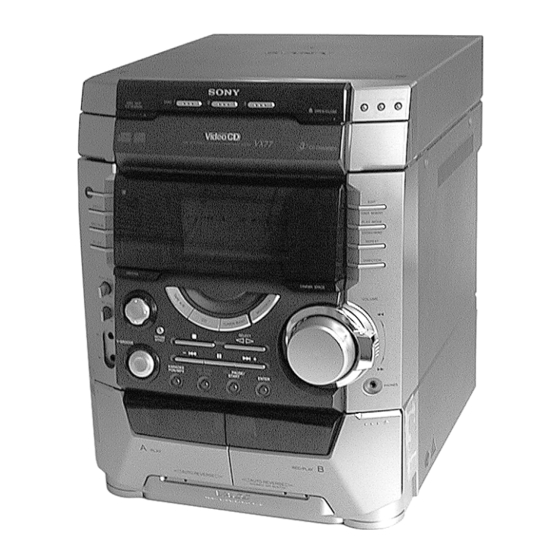
HCD-VX99 is the tuner, deck, CD and amplifier
section in MHC-VX99.
TE
L 13942296513
Amplifier section
The following measured at AC 120, 220, 240V
50/60 Hz
DIN power output (rated) 220 + 220 W
Continuous RMS power output (reference)
Inputs
MD/VIDEO (AUDIO) IN: voltage 450 mV/250 mV,
(phono jacks)
MIC:
(phone jack)
Outputs
VIDEO OUT:
(Phono jack)
S-VIDEO OUT:
(4 pin/mini-DIN jack)
PHONES:
(stereo mini jack)
FRONT SPEAKER:
www
.
http://www.xiaoyu163.com
TAPE DECK
VIDEO CD/CD player section
System
Laser
(4 Ω at 1 kHz, DIN)
300 + 300 W
(4 Ω at 1 kHz,
Laser output
10% THD)
impedance 47 kΩ
sensitivity 1 mV,
impedance 10 kΩ
Frequency response
Wavelength
max. output level 1 Vp-p,
Signal-to-noise ratio
unbalanced, Sync
Dynamic range
negative, load impedance
Video color system format
75 Ω
Y: 1 Vp-p, unbalanced
CD OPTICAL DIGITAL OUT
Sync negative
(Square optical connector jack, rear panel)
C: 0.286 Vp-p
Wavelength
load impedence 75 Ω
Output Level
accepts headphones of 8
Ω or more
accepts impedance of 4 to
16 Ω
x
ao
u163
y
i
http://www.xiaoyu163.com
HCD-VX99
2 9
8
Model Name Using Similar Mechanism
CD
CD Mechanism Type
SECTION
Base Unit Type
Optical Pick-up Type
Model Name Using Similar Mechanism
Q Q
SECTION
Tape Transport Mechanism Type
3
6 7
1 3
SPECIFICATIONS
Compact disc and digital
audio system
Semiconductor laser
(λ=780nm)
Emission duration:
continuous
Max. 44.6 µ W*
*This output is the value
measured at a distance of
200 mm from the
objective lens surface on
the Optical Pick-up Block
with 7 mm aperture.
2 Hz – 20 kHz (±0.5 dB)
780 – 790 nm
More than 90 dB
More than 90 dB
NTSC, PAL
660 nm
–18 dBm
COMPACT DISC DECK RECEIVER
.
9 4
2 8
HCD-VX77/VX77J
CDM58-K2BD37A
BU-K2BD37A
KSM-213DAP/Z-NP
HCD-VX77/VX77J
TCM-230PWR11
1 5
0 5
8
2 9
9 4
Tape player section
Recording system
4-track 2-channel stereo
Frequency response
40 – 13,000 Hz (±3 dB),
(DOLBY NR OFF)
using Sony TYPE I
cassette
Tuner section
FM stereo, FM/AM superheterodyne tuner
FM tuner section
Tuning range
87.5 – 108.0 MHz
Antenna
FM lead antenna
75 Ω unbalanced
Antenna terminals
Intermediate frequency
10.7 MHz
AM tuner section
Tuning range
Middle East model:
531 – 1,602 kHz
(with the interval set at 9
kHz)
Other models:
531 – 1,602 kHz
(with the interval set at 9
kHz)
530 – 1,710 kHz
(with the interval set at 10
kHz)
Antenna
AM loop antenna
Antenna terminals
External antenna terminal
Intermediate frequency
450 kHz
— Continued on next page —
m
co
9 9
E Model
2 8
9 9
1
Advertisement
Table of Contents

Subscribe to Our Youtube Channel
Related Manuals for Sony HCD-VX99


Summary of Contents for Sony HCD-VX99
- Page 1 HCD-VX99 3 7 63 1515 0 SERVICE MANUAL E Model HCD-VX99 is the tuner, deck, CD and amplifier section in MHC-VX99. Model Name Using Similar Mechanism HCD-VX77/VX77J CD Mechanism Type CDM58-K2BD37A SECTION Base Unit Type BU-K2BD37A Optical Pick-up Type...
-
Page 2: Table Of Contents
http://www.xiaoyu163.com 3 7 63 1515 0 TABLE OF CONTENTS General Power requirements 120 V, 220 V or 230 - 240 V AC, 50/60 Hz 1. SERVICE NOTE ······························································· 4 Adjustable with voltage selector 2. GENERAL ·········································································· 5 Power consumption 300 W 3. - Page 3 COMPONENTS IDENTIFIED BY MARK 0 OR DOTTED LINE WITH MARK 0 ON THE SCHEMATIC DIAGRAMS AND IN THE PARTS LIST ARE CRITICAL TO SAFE OPERATION. REPLACE THESE COMPONENTS WITH SONY PARTS WHOSE PART NUMBERS APPEAR AS SHOWN IN THIS MANUAL OR IN SUPPLEMENTS PUBLISHED BY SONY.
-
Page 4: Service Note
http://www.xiaoyu163.com SECTION 1 SERVICE NOTE 3 7 63 1515 0 Note for installing the panel board 2 Panel board Hot melt Screw hole 1 Cut the eleven melted-connection points with a cutting plier. Attach the panel board with six screws (+BVTP 2.6 × 8 ) after the board is removed once. -
Page 5: General
http://www.xiaoyu163.com SECTION 2 3 7 63 1515 0 GENERAL 2 3 4 qk qj DISC SKIP EX-CHANGE button ECHO LEVEL knob DISC 1 button and indicator EQ EDIT button DISC 2 button and indicator SPECTRUM button L 13942296513 DISC 3 button and indicator DISPLAY button Z OPEN/CLOSE button ?/1 button and indicator... - Page 6 http://www.xiaoyu163.com 3 7 63 1515 0 This section is extracted from instruction manual. L 13942296513 u163 http://www.xiaoyu163.com...
-
Page 7: Disassembly
http://www.xiaoyu163.com SECTION 3 3 7 63 1515 0 DISASSEMBLY Note : Follow the disassembly procedure in the numerical order given. 3-1. UPPER CASE (TOP) 9Two screws (+BVTP 3 × 10) Upper case (Top) 5Two screws (Case) 7Two screws (+BVTP 3 × 10) Claw Side panel R Side panel L... - Page 8 http://www.xiaoyu163.com 3 7 63 1515 0 3-3. FRONT PANEL SECTION 0Two screws (+BVTP 2.6 × 8) 8Connector (CN201) CD mechanism deck (CDM58) 4Screw (+BVTP 3 × 10) Connector (CN601) 1Flat type wire (CN304) 5Screw (+BVTP 3 × 10) 2Connector (CN1) 9Connector (CN202) 3Connector (CN2) Front panel section...
- Page 9 http://www.xiaoyu163.com 3 7 63 1515 0 3-5. PANEL BOARD 0Three claws 9Three screws (+BVTP 2.6 × 8) 7Knob(MIC) qaCD Switch board 6Spring qfPanel board 2Two screws (+BVTP 2.6 × 8) qdFive claws 3Two bosses & four pins 5FR knob qsCut the eleven melted-connection points with a cutting plier. 4Bracket (FR) Note: When attching the panel board, refer to "Service Note"...
- Page 10 http://www.xiaoyu163.com 3 7 63 1515 0 3-7. MAIN BOARD AND AMP BOARD 4Three screws (+BVTP 3 × 8) 7Heat sink 6Two screws (+BVTP 3 × 8) 5Power AMP board Connector(CN502) 3Two screws (+BVTP 3 × 16) Connector (CN503) 2Main board 1Two screws (+BVTP 3 ×...
- Page 11 http://www.xiaoyu163.com 3 7 63 1515 0 3-9. BASE UNIT 4Two insulators Base unit 1Flat type wire (CN101) 5Two insulators 2Four screws (+PTPWH 2.6) 3-10. DRIVER BOARD, MOTOR BOARD SENSOR BOARD AND VIDEO BOARD L 13942296513 9Screw (+PTPWH 2.6 × 8) 4Three screws (+BVTP 2.6 ×...
-
Page 12: Test Mode
http://www.xiaoyu163.com SECTION 4 TEST MODE 3 7 63 1515 0 [MC Cold Reset] [Change-over of MW Tuner Step between 9 kHz and • The cold reset clears all data including preset data stored in the 10 kHz] RAM to initial conditions. Execute this mode when returning •... - Page 13 http://www.xiaoyu163.com 3 7 63 1515 0 [MC Test Mode] • This mode is used to check operations of the respective sections of Amplifier, Tuner, CD and Tape. Procedure: Press the ?/1 button to turn on the set. Press the three buttons of x , ENTER and DISC 3 simultaneously.
- Page 14 http://www.xiaoyu163.com 3 7 63 1515 0 [Aging Mode] This mode can be used for operation check of CD section and tape deck section. • If an error occurred: The aging operation stops and display status. • If no error occurs: The aging operation continues repeatedly.
- Page 15 http://www.xiaoyu163.com 3 7 63 1515 0 2) Operation during aging mode In the aging mode, the program is executed in the following sequence. (1) The disc tray opens and closes. (2) The mechanism accesses DISC 2 and makes an attempt to read TOC.
- Page 16 http://www.xiaoyu163.com 3 7 63 1515 0 VIDEO CD COLOR-BARS MODE On this mode, the data of the color-bars signal as a picture signal and the 1kHz sine wave signal as a sound signal are output by the mechanism control microcomputer (IC502) for video CD signal check. When measurement of the voltage and waveform on the VIDEO board, perform it in this mode.
-
Page 17: Mechanical Adjustments
http://www.xiaoyu163.com SECTION 5 SECTION 6 MECHANICAL ADJUSTMENTS ELECTRICAL ADJUSTMENTS 3 7 63 1515 0 Precaution DECK SECTION 0 dB=0.775 V 1. Clean the following parts with a denatured alcohol-moistened swab: 1. Demagnetize the record/playback head with a head record/playback heads pinch rollers demagnetizer. - Page 18 http://www.xiaoyu163.com 3 7 63 1515 0 2. Turn the adjustment screw and check output peaks. If the peaks DECK B Tape Speed Adjustment do not match for L-CH and R-CH, turn the adjustment screw Note: Start the Tape Speed adjustment as below after setting to the test so that outputs match within 1dB of peak.
- Page 19 http://www.xiaoyu163.com 3 7 63 1515 0 DECK B REC Bias Adjustment 4. Mode: Record Procedure: INTRODUCTION MD/VIDEO (AUDIO) IN When set to the test mode performed in Tape Speed Adjustment, 315 Hz, 50 mV (–23.8 dB) AF OSC when the tape is rewound after recording, the “REC memory mode” blank tape 600 Ω...
- Page 20 http://www.xiaoyu163.com 3 7 63 1515 0 FM Tuned Level Adjustment CD SECTION FM RF SSG Note : 1. CD Block is basically designed to operate without adjustment. 75 Ω coaxial Therefore, check each item in order given. 2. Use YEDS-18 disc (3-702-101-01) unless otherwise indicated. 3.
- Page 21 http://www.xiaoyu163.com 3 7 63 1515 0 Note: Clear RF signal waveform means that the shape “◊” can be clearly distinguished at the center of the waveform. RF signal waveform VOLT/DIV : 200mV TIME/DIV : 500ns level : 1.45 ± 0.3Vp-p E-F Balance (1 Track jump) Check oscilloscope BD board...
- Page 22 http://www.xiaoyu163.com 3 7 63 1515 0 Adjustment Location : [ BD BOARD ] — SIDE B — (RF) IC102 (VC) (AGCCON) (DGND) (FEO) (TEO) (AGND) (IOP) L 13942296513 VIDEO SECTION Frequency adjustment frequency counter Connect the frequency counter to check point of the VIDEO VIDEO board board.
-
Page 23: Diagrams
HCD-VX99 SECTION 7 DIAGRAMS 3 7 6 3 1 5 1 5 0 7-1. CIRCUIT BOARD LOCATION THIS NOTE IS COMMON FOR PRINTED WIRING BOARDS AND SCHEMATIC DIAGRAMS. (In addition to this, the necessary note is printed in each block.) - Page 24 HCD-VX99 3 7 6 3 1 5 1 5 0 Waveforms – BD SECTION – – VIDEO SECTION – – PANEL BOARD – – MAIN BOARD – IC101 t; IC502 qd IC509 ql IC401 qa IC601 oa T301 4...
-
Page 25: Block Diagrams
HCD-VX99 7-2. BLOCK DIAGRAMS 3 7 6 3 1 5 1 5 0 AM/FM IF MPX TM601 LPF601 FE602 Q602 IC601 – TUNER/CD SECTION – CF601 CF602 RF IF BUFFER L-CH • RCH is omitted ANT IN IF OUT... - Page 26 HCD-VX99 3 7 6 3 1 5 1 5 0 – VIDEO SECTION – D-RAM IC507 IC506 16 - 19 22 - 26 2 - 10 31 - 39 13 - 15 17 - 21 25 4 28 29 3 2 30...
- Page 27 HCD-VX99 3 7 6 3 1 5 1 5 0 – MAIN SECTION – J102 SURROUND SPEAKER R CH INPUT SELECT TONE/VOL CONT IC101 IC102 IC501 TM801 TUNER L-CH SECTION IN2A VOL OUT2 (Page 25) POWER SPEAKER Q504,505 Q861...
-
Page 28: Printed Wiring Board - Bd Section
HCD-VX99 3 7 6 3 1 5 1 5 0 7-3. PRINTED WIRING BOARD – BD SECTION – • See page 23 for Circuit Boards Location. 1 3 9 4 2 2 9 6 5 1 3 w w w u 1 6 3 http://www.xiaoyu163.com... -
Page 29: Schematic Diagram - Bd Section
HCD-VX99 3 7 6 3 1 5 1 5 0 7-4. SCHEMATIC DIAGRAM – BD SECTION – • See page 24 for Waveforms. • See page 57 for IC Block Diagrams. • See page 48 for IC Pin Function. -
Page 30: Printed Wiring Board - Video Section
HCD-VX99 3 7 6 3 1 5 1 5 0 7-5. PRINTED WIRING BOARD – VIDEO SECTION – • See page 23 for Circuit Boards Location. 1 3 9 4 2 2 9 6 5 1 3 • Semiconductor Location w w w Ref. -
Page 31: Schematic Diagram - Video (1/3) Section
HCD-VX99 3 7 6 3 1 5 1 5 0 7-6. SCHEMATIC DIAGRAM – VIDEO (1/3) SECTION – • See page 24 for Waveforms. • See page 49 for IC Pin Function. 1 3 9 4 2 2 9 6 5 1 3... -
Page 32: Schematic Diagram - Video (2/3) Section
HCD-VX99 7-7. SCHEMATIC DIAGRAM – VIDEO (2/3) SECTION – • See page 24 for Waveforms. • See page 51 for IC Pin Function. • See page 30 for Printed Wiring Board. 3 7 6 3 1 5 1 5 0... -
Page 33: Schematic Diagram - Video (3/3) Section
HCD-VX99 7-8. SCHEMATIC DIAGRAM – VIDEO (3/3) SECTION – • See page 24 for Waveforms. • See page 60 for IC Block Diagrams. • See page 30 for Printed Wiring Board. 3 7 6 3 1 5 1 5 0... -
Page 34: Printed Wiring Board - Main Section
HCD-VX99 7-9. PRINTED WIRING BOARD – MAIN SECTION – • See page 23 for Circuit Boards Location. 3 7 6 3 1 5 1 5 0 • Semiconductor Location Ref. No. Location (Page 30) (Page 44) D501 TO DRIVER BOARD... -
Page 35: Schematic Diagram - Main (1/3) Section
HCD-VX99 3 7 6 3 1 5 1 5 0 7-10. SCHEMATIC DIAGRAM – MAIN (1/3) SECTION – • See page 59 for IC Block Diagrams. 1 3 9 4 2 2 9 6 5 1 3 w w w u 1 6 3 http://www.xiaoyu163.com... -
Page 36: Schematic Diagram - Main (2/3) Section
HCD-VX99 3 7 6 3 1 5 1 5 0 7-11. SCHEMATIC DIAGRAM – MAIN (2/3) SECTION – • See page 24 for Waveforms. • See page 58 for IC Block Diagrams. • See page 54 for IC Pin Function. • See page 34 for Printed Wiring Board. -
Page 37: Schematic Diagram - Main (3/3) Section
HCD-VX99 3 7 6 3 1 5 1 5 0 7-12. SCHEMATIC DIAGRAM – MAIN (3/3) SECTION – • See page 34 for Printed Wiring Board. 1 3 9 4 2 2 9 6 5 1 3 w w w u 1 6 3 http://www.xiaoyu163.com... -
Page 38: Printed Wiring Board - Power Amp Section
HCD-VX99 3 7 6 3 1 5 1 5 0 7-13. PRINTED WIRING BOARD – POWER AMP SECTION – • See page 23 for Circuit Boards Location. (Page 46) (Page 34) (Page 34) • Semiconductor Location Ref. No. Location... -
Page 39: Schematic Diagram - Power Amp Section
HCD-VX99 3 7 6 3 1 5 1 5 0 7-14. SCHEMATIC DIAGRAM – POWER AMP SECTION – 1506 NO505 1 3 9 4 2 2 9 6 5 1 3 w w w u 1 6 3 http://www.xiaoyu163.com... -
Page 40: Printed Wiring Board - Panel Section
HCD-VX99 7-15. PRINTED WIRING BOARD – PANEL SECTION – • See page 23 for Circuit Boards Location. 3 7 6 3 1 5 1 5 0 • Semiconductor Location Ref. No. Location D601 D602 D603 D611 D612 D613 D614... -
Page 41: Schematic Diagram - Panel Section
HCD-VX99 3 7 6 3 1 5 1 5 0 7-16. SCHEMATIC DIAGRAM – PANEL SECTION – • See page 24 for Waveforms. • See page 58 for IC Block Diagrams. • See page 56 for IC Pin Function. -
Page 42: Printed Wiring Board - Leaf Sw Section
HCD-VX99 3 7 6 3 1 5 1 5 0 7-17. PRINTED WIRING BOARD – LEAF SW SECTION – • See page 23 for Circuit Boards Location. • Semiconductor Location Ref. No. Location D1001 D1002 IC1001 IC1002 Q1001 1 3 9 4 2 2 9 6 5 1 3... -
Page 43: Schematic Diagram - Leaf Sw Section
HCD-VX99 3 7 6 3 1 5 1 5 0 7-18. SCHEMATIC DIAGRAM – LEAF SW SECTION – 1 3 9 4 2 2 9 6 5 1 3 w w w u 1 6 3 http://www.xiaoyu163.com... -
Page 44: Printed Wiring Board - Driver Section
HCD-VX99 3 7 6 3 1 5 1 5 0 7-19. PRINTED WIRING BOARD – DRIVER SECTION – • See page 23 for Circuit Boards Location. • Semiconductor Location Ref. No. Location D701 IC701 IC711 1 3 9 4 2 2 9 6 5 1 3... -
Page 45: Schematic Diagram - Driver Section
HCD-VX99 3 7 6 3 1 5 1 5 0 7-20. SCHEMATIC DIAGRAM – DRIVER SECTION – • See page 58 for IC Block Diagrams. 1 3 9 4 2 2 9 6 5 1 3 w w w u 1 6 3 http://www.xiaoyu163.com... -
Page 46: Printed Wiring Board - Trans Section
HCD-VX99 3 7 6 3 1 5 1 5 0 7-21. PRINTED WIRING BOARD – TRANS SECTION – • See page 23 for Circuit Boards Location. F973 F972 (Page 38) 1 3 9 4 2 2 9 6 5 1 3... -
Page 47: Schematic Diagram - Trans Section
HCD-VX99 3 7 6 3 1 5 1 5 0 7-22. SCHEMATIC DIAGRAM – TRANS SECTION – CN978 1 3 9 4 2 2 9 6 5 1 3 w w w u 1 6 3 http://www.xiaoyu163.com... -
Page 48: Ic Pin Function
HCD-VX99 3 7 6 3 1 5 1 5 0 7-23. IC PIN FUNCTIONS • IC101 DIGITAL SIGNAL PROCESSOR (CXD3008Q) (BD Board) Pin No. Pin Name Function Pin No. Pin Name Function DVDD0 — Digital power supply Tracking error signal input... - Page 49 http://www.xiaoyu163.com 3 7 63 1515 0 • IC502 MPEG DECODER, MECHANISM CONTROL (M30624MCA-A34FP) (VIDEO Board (1/3)) Pin No. Pin Name Function SENSE Internal state (SENSE) monitor input (IC101) SENSE CLK Serial data reading clock output (IC101) RESOLUTION Serial data output (IC101) CROMA LEVEL Lach output (IC101) DSP CLK...
- Page 50 http://www.xiaoyu163.com 3 7 63 1515 0 Pin No. Pin Name Function BUS XWRL Not used LO. BOOST Not used AUDIO MUTE Audio mute output “L” : mute (Not used) LOAD OUT Not used LOAD IN Not used INSW Not used OUTSW Not used MODEL 1...
- Page 51 http://www.xiaoyu163.com 3 7 63 1515 0 • IC505 CD DECODER, SYSTEM CONTROL (CL680T-D1) (VIDEO Board (2/3)) Pin No. Pin Name Function – Not used – Ground CD-BCK CD Decode bit clock CD-DATA CD Decode data CD-LRCK CD Decode Left or Right channel selection clock CD-C2PO CD Decode C2 error data –...
- Page 52 http://www.xiaoyu163.com 3 7 63 1515 0 Pin No. Pin Name Function Address data from CL680 to Microcode ROM/DRAM – Ground Address data from CL680 to Microcode ROM/DRAM VDD3 – +3.3V Power supply Address data from CL680 to Microcode ROM/DRAM Address data from CL680 to Microcode ROM/DRAM Address data from CL680 to Microcode ROM/DRAM –...
- Page 53 http://www.xiaoyu163.com 3 7 63 1515 0 Pin No. Pin Name Function PGIO0 Not used PGIO8 Not used PGIO2/VSYNC/CSYNC Vertical synchronized signal of video signal AVDD PLL – +3.3V Power supply – Not used – Not used – Not used AGND PLL –...
- Page 54 http://www.xiaoyu163.com 3 7 63 1515 0 • IC401 MASTER CONTROL (M30622MAA-A59FP) (MAIN BOARD) Pin No. Pin Name Description SURROUND 1 Surround control signal output SURROUND 2 Surround control signal output SURROUND 3 Surround control signal output 498-DATA Data signal output for IC101 (M61504FP) 498-CLK Clock signal output for IC101 (M61504FP) Not used.
- Page 55 http://www.xiaoyu163.com 3 7 63 1515 0 Pin No. Pin Name Description Not used. Not used. Not used. Not used. Not used. Not used. A TRIG A deck trigger control signal output.H=ON, L-OFF B TRIG B deck trigger control signal output.H=ON, L-OFF CAPM-H/L Capstan motor High/Low speed control signal output.
- Page 56 http://www.xiaoyu163.com 3 7 63 1515 0 • IC601 DISPLAY CONTROL (TMP88CP77F-1A22) (PANEL BOARD) Pin No. Pin No. Pin Name Pin Name Description Description VOLUME A VOLUME A VOLUME A signal input. VOLUME A signal input. VOLUME B VOLUME B VOLUME B signal input. VOLUME B signal input.
-
Page 57: Ic Block Diagrams
http://www.xiaoyu163.com 3 7 63 1515 0 7-24. IC BLOCK DIAGRAMS IC102 BA5982FM (BD BOARD) BIAS IN PreVcc OPIN1 + OPIN4 + OPIN1 – OPIN4 – OPOUT1 OPOUT4 OPIN2 + OPIN3 + OPIN3 – OPIN2 – OPOUT2 OPOUT3 STAND BY STAND BY STBY1 STBY2 CH1 2 3... - Page 58 http://www.xiaoyu163.com 3 7 63 1515 0 IC103 LA2615 (MAIN BOARD) IC602 BA3830F-E2 (PANEL BOARD) REFFERENCE RESET 18 RESET CURRENT REFFERENCE 17 f01 CURRENT ANALOG LEVEL ON/OFF SURROUND LINE 16 f02 VREF LINE 15 f03 13 f05 RESET 12 f06 BIAS 11 REC Bias LEVEL...
- Page 59 http://www.xiaoyu163.com 3 7 63 1515 0 IC601 BA1450 (MAIN BOARD) AM IF VREG DECODER DRIVER COMP IC302 µPC1330HA (MAIN BOARD) INVERTER L 13942296513 COMPARATER SW R1 SW P1 CONT SW P2 SW R2 IC651 LC72130 (MAIN BOARD) SWALLOW COUNTER 1/16.1/17 4bits POWER REFERENCE RESET...
- Page 60 http://www.xiaoyu163.com 3 7 63 1515 0 IC302 NJM2255M (VIDEO BOARD) IC303 NJM2209M (VIDEO BOARD) SATURATION +Ø ADJUST (COLOR BURST) HUE ADJUST SATURATION SECONDARY LOWER CLAMP ADJUST DIFFERENTIATION LIMITER SYNC –X (COLOR BURST) GAIN ADJ CHIP SWITCH CONTROL LOWER LIMITER IC304 BA7665FS (VIDEO BOARD) Mute MUTEA...
-
Page 61: Exploded Views
http://www.xiaoyu163.com SECTION 8 EXPLODED VIEWS 3 7 63 1515 0 NOTE: • -XX, -X mean standardized parts, so they may • Abbreviation The components identified by mark 0 or have some differences from the original one. EA : Middle East model dotted line with mark 0 are critical for safety. -
Page 62: Panel Section
X-4952-794-1 TC HOLDER (R) ASSY(EA) 4-225-053-01 SPRING R 4-225-032-11 VOL KNOB 4-224-584-11 HOLDER (FL) A-4428-450-A CD SWITCH BOARD, COMPLETE A-4428-457-A PANEL BOARD, COMPLETE 4-962-708-81 EMBLEM (4-A), SONY 4-951-620-01 SCREW (2.6X8), +BVTP 4-225-033-01 FR KNOB 4-224-578-11 KNOB(MIC) X-4952-676-1 FRONT PANEL ASSY 4-225-052-01 SPRING L... -
Page 63: Main Board Section
http://www.xiaoyu163.com 3 7 63 1515 0 8-3. MAIN BOARD SECTION not supplied L 13942296513 not supplied The components identified by mark 0 or dotted line with mark 0 are critical for safety. Replace only with part number specified. Ref. No. Part No. -
Page 64: Tape Mechanism Deck Section
http://www.xiaoyu163.com 3 7 63 1515 0 8-4. TAPE MECHANISM DECK SECTION Note: Two different types of tape mechanism are used depending on models. They maintain compatibility as an entire mechanism even though there are some different parts are used. L 13942296513 Ref. -
Page 65: Cd Mechanism Deck Section (Cdm58-K2Bd37A)
http://www.xiaoyu163.com 3 7 63 1515 0 8-5. CD MECHANISM DECK SECTION (CDM58-K2BD37A) M721 not supplied L 13942296513 not supplied not supplied BU-K2BD37 not supplied Ref. No. Part No. Description Remarks Ref. No. Part No. Description Remarks 4-933-134-11 SCREW (+PTPWH M2.6X8) 4-221-688-01 PULLEY (B), CHUCKING 4-221-679-01 CAM (RELAY) 1-471-035-11 MAGNET ASSY... -
Page 66: Base Unit Section (Bu-K2Bd37A)
http://www.xiaoyu163.com 3 7 63 1515 0 8-6. BASE UNIT SECTION (BU-K2BD37A) L 13942296513 The components identified by mark 0 or dotted line with mark 0 are critical for safety. Replace only with part number specified. Ref. No. Part No. Description Remark 0 251 8-820-116-01 OPTICAL PICK-UP BLOCK KSM-213DAP/Z-NP... -
Page 67: Electrical Parts List
http://www.xiaoyu163.com SECTION 9 ELECTRICAL PARTS LIST 3 7 63 1515 0 NOTE: • Due to standardization, replacements in the • COILS Ref. No. Part No. Description Remarks Ref. No. Part No. Description Remarks When indicating parts by reference number, parts list may be different from the parts uH: µH please include the board name. - Page 68 http://www.xiaoyu163.com CD SWITCH DRIVER HEAD (A) 3 7 63 1515 0 Ref. No. Part No. Description Remarks Ref. No. Part No. Description Remarks R147 1-216-041-00 METAL CHIP 1/10W < RESISTOR > R148 1-216-001-00 METAL CHIP 1/10W R149 1-216-003-11 RES-CHIP 1/10W R685 1-249-417-11 CARBON 1/4W F...
- Page 69 http://www.xiaoyu163.com HEAD (B) LEAF SW MAIN 3 7 63 1515 0 Ref. No. Part No. Description Remarks Ref. No. Part No. Description Remarks 1-676-221-11 HEAD (B) BOARD < CAPACITOR > ************** C101 1-163-001-11 CERAMIC CHIP 220PF 1-564-722-11 PIN, CONNECTOR (SMALL TYPE) 6P C102 1-126-961-11 ELECT 2.2uF...
- Page 70 http://www.xiaoyu163.com MAIN 3 7 63 1515 0 Ref. No. Part No. Description Remarks Ref. No. Part No. Description Remarks C204 1-126-961-11 ELECT 2.2uF 20.00% 50V C363 1-163-017-00 CERAMIC CHIP 0.0047uF 5% C205 1-163-033-91 CERAMIC CHIP 0.022uF C368 1-126-964-11 ELECT 10uF 20.00% 50V C206 1-126-961-11 ELECT...
- Page 71 http://www.xiaoyu163.com MAIN 3 7 63 1515 0 Ref. No. Part No. Description Remarks Ref. No. Part No. Description Remarks C634 1-163-016-00 CERAMIC CHIP 0.0039uF 10% * CN891 1-564-506-11 PLUG, CONNECTOR 3P C635 1-163-016-00 CERAMIC CHIP 0.0039uF 10% CN901 1-778-982-21 CONNECTOR, BOARD TO BOARD 13P C636 1-163-021-91 CERAMIC CHIP 0.01uF...
- Page 72 http://www.xiaoyu163.com MAIN 3 7 63 1515 0 Ref. No. Part No. Description Remarks Ref. No. Part No. Description Remarks IC303 8-759-656-83 IC NJM4580MD-TE JR606 1-216-296-91 SHORT IC304 8-759-656-83 IC NJM4580MD-TE JR607 1-216-295-91 SHORT IC401 8-759-677-42 IC M30622MAA-A59 JR608 1-216-296-91 SHORT IC501 8-759-635-63 IC M51943BSL-TP JR611...
- Page 73 http://www.xiaoyu163.com MAIN 3 7 63 1515 0 Ref. No. Part No. Description Remarks Ref. No. Part No. Description Remarks Q823 8-729-216-22 TRANSISTOR 2SA812-T1-M5M6 R173 1-216-073-00 METAL CHIP 1/10W Q824 8-729-113-13 TRANSISTOR FA1A4M-T1L33 R175 1-216-073-00 METAL CHIP 1/10W Q825 8-729-120-28 TRANSISTOR 2SC1623-T1-L5L6 R181 1-216-049-91 RES-CHIP...
- Page 74 http://www.xiaoyu163.com MAIN 3 7 63 1515 0 Ref. No. Part No. Description Remarks Ref. No. Part No. Description Remarks R366 1-216-061-00 METAL CHIP 3.3K 1/10W R499 1-216-025-91 RES-CHIP 1/10W R367 1-216-089-91 RES-CHIP 1/10W R501 1-216-073-00 METAL CHIP 1/10W R368 1-216-061-00 METAL CHIP 3.3K 1/10W R502...
- Page 75 http://www.xiaoyu163.com MAIN MOTOR PANEL 3 7 63 1515 0 Ref. No. Part No. Description Remarks Ref. No. Part No. Description Remarks R823 1-216-222-00 RES-CHIP 1/8W < VIBRATOR > R824 1-216-073-00 METAL CHIP 1/10W R825 1-216-061-00 METAL CHIP 3.3K 1/10W X401 1-567-098-41 VIBRATOR, CRYSTAL 32.768KHz R826 1-216-085-00 METAL CHIP...
- Page 76 http://www.xiaoyu163.com PANEL 3 7 63 1515 0 Ref. No. Part No. Description Remarks Ref. No. Part No. Description Remarks C662 1-162-282-31 CERAMIC 100PF C767 1-162-282-31 CERAMIC 100PF C663 1-162-282-31 CERAMIC 100PF C768 1-162-282-31 CERAMIC 100PF C664 1-162-282-31 CERAMIC 100PF C769 1-162-282-31 CERAMIC 100PF C665...
- Page 77 http://www.xiaoyu163.com PANEL 3 7 63 1515 0 Ref. No. Part No. Description Remarks Ref. No. Part No. Description Remarks < TRANSISTOR > R653 1-249-411-11 CARBON 1/4W R654 1-249-413-11 CARBON 1/4W F Q604 8-729-900-80 TRANSISTOR BA1A4M-TP R655 1-249-415-11 CARBON 1/4W F Q605 8-729-900-80 TRANSISTOR BA1A4M-TP...
- Page 78 http://www.xiaoyu163.com PANEL POWER AMP 3 7 63 1515 0 Ref. No. Part No. Description Remarks Ref. No. Part No. Description Remarks R739 1-249-441-11 CARBON 100K 1/4W C504 1-104-665-11 ELECT 100uF 20.00% 10V R740 1-249-417-11 CARBON 1/4W F C507 1-136-495-11 MYLAR 0.068uF 5.00% 50V R741...
- Page 79 http://www.xiaoyu163.com POWER AMP SENSOR TRANS VIDEO 3 7 63 1515 0 Ref. No. Part No. Description Remarks Ref. No. Part No. Description Remarks < RESISTOR > < IC > R501 1-249-417-11 CARBON 1/4W F IC711 8-749-016-76 IC RPI-321 R502 1-249-438-11 CARBON 1/4W R503 1-249-413-11 CARBON...
- Page 80 http://www.xiaoyu163.com VIDEO 3 7 63 1515 0 Ref. No. Part No. Description Remarks Ref. No. Part No. Description Remarks C308 1-163-263-11 CERAMIC CHIP 330PF 5.00% 50V C574 1-163-235-11 CERAMIC CHIP 22PF 5.00% 50V C309 1-163-263-11 CERAMIC CHIP 330PF 5.00% 50V C576 1-163-235-11 CERAMIC CHIP 22PF...
- Page 81 http://www.xiaoyu163.com VIDEO 3 7 63 1515 0 Ref. No. Part No. Description Remarks Ref. No. Part No. Description Remarks L513 1-469-145-21 FERRITE R543 1-216-685-11 METAL CHIP 0.5% 1/10W R544 1-216-659-11 METAL CHIP 2.2K 0.5% 1/10W < TRANSISTOR > R545 1-216-025-91 RES-CHIP 1/10W R546 1-216-049-91 RES-CHIP...
- Page 82 HCD-VX99 3 7 63 1515 0 Ref. No. Part No. Description Remarks Ref. No. Part No. Description Remarks L 13942296513 u163 Sony Corporation 9-929-237-11 2000D0923-1D Audio Entertainment Group Printed in Japan © 2000.4 Published by HA Quality Assurance Dept.
Need help?
Do you have a question about the HCD-VX99 and is the answer not in the manual?
Questions and answers