
Related Manuals for Portwell WADE-8044 Series


Summary of Contents for Portwell WADE-8044 Series
- Page 1 WADE-8044 Series Mini-ITX Board User's Manual Version 1.0 Copyright © Portwell, Inc., 2008. All rights reserved. All other brand names are registered trademarks of their respective owners.
-
Page 2: Table Of Contents
Preface Table of Contents How to Use This Manual Chapter 1 System Overview.......................1-1 1.1 Introduction..........................1-1 1.2 Check List ............................. 1-1 1.3 Product Specification ........................1-2 1.3.1 Mechanical Drawing......................1-4 1.4 System Architecture ........................1-5 Chapter 2 Hardware Configuration ...................2-1 2.1 Jumper Setting .......................... -
Page 3: How To Use This Manual
Preface How to Use This Manual The manual describes how to configure your WADE-8044 system board to meet various operating requirements. It is divided into five chapters, with each chapter addressing a basic concept and operation of Single Host Board. Chapter 1: System Overview. -
Page 4: Chapter 1 System Overview
Flash ROM is used to make the BIOS update easier. One 20-pin standard connector is designed to support ATX power function. All of these features make WADE-8044 series excellent in stand-alone applications. Check List The WADE-8044 package should cover the following basic items... -
Page 5: Product Specification
System Overview Product Specification - Support Intel Pentium M / Celeron® M processor ® - CPU bus clock: 400 MHz Chipset Intel® 910GMLE GMCH and ICH6-M Main Memory - Two 240-pin DIMM socket - Support dual channel memory DDR2 400MHz up to 2GB System BIOS - AWARD BIOS Super I/O Winbond W83627DHG-E and Fintek F81216DG... - Page 6 System Overview - One DVI-D connector for DVI display interface - One LVDS connector for 24-bit LVDS panel display interface (Optional) - CRT: Support maximum resolution up to 2048 x 1536 - 18-bit LVDS: Support maximum resolution up to 1400 x 1050 - DVI: Support maximum resolution up to 1600 x 1200 - 24-bit LVDS: Support maximum resolution up to 1600 x 1200 (Optional) On-board Ethernet Function...
-
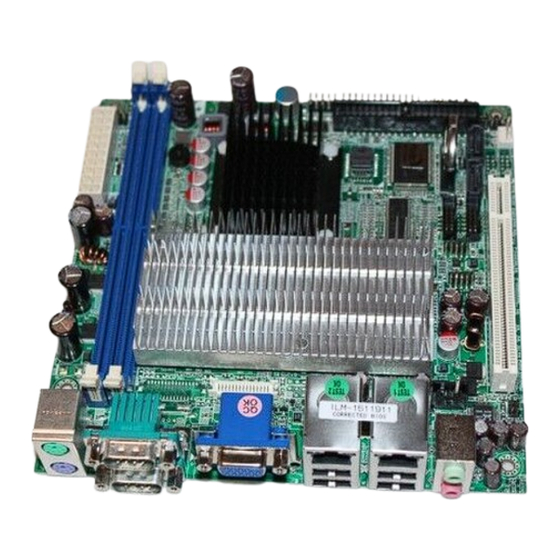
Page 7: Mechanical Drawing
System Overview 1.3.1 Mechanical Drawing WADE-8044 Mechanical Drawing WADE-8044 User’s Manual... -
Page 8: System Architecture
System Overview System Architecture All of details operating relations are shown in WADE-8044 System Block Diagram. Pentium M/Celeron M IMVP VRM CK410 Processor AGTL+BUS FSB533/400MHz DIMM DDR2 Channel A 533/400MHz 18 -bit LVDS 915GME/910GMLE 24-bit LVDS LVDS GMCH SDVOB DIMM DDR2 (optional) Transmitter Channel B... -
Page 9: Chapter 2 Hardware Configuration
Hardware Configuration Chapter 2 Hardware Configuration This chapter indicates jumpers’, headers’ and connectors’ locations. Users may find useful information related to hardware settings in this chapter. The default settings are indicated with a star sign ( ). Jumper Setting In the following sections, Short means covering a jumper cap over jumper pins; Open or N/C (Not Connected) means removing a jumper cap from jumper pins. - Page 10 Hardware Configuration The jumper settings are listed as follows: JP1 : 24-bit LVDS Backlight Enable Select (Optional) Function 1-3,2-4 Short +5V(HIGH) 1-3,4-6 Short +12V(HIGH) 3-5,2-4 Short +5V(LOW) 3-5,4-6 Short +12V(LOW) JP2 : 24-bit LVDS VDD Select (Optional) Function 2-4 Short +3.3V 4-6 Short 3-4 Short...
- Page 11 Hardware Configuration JP8 : Banias or Dothan voltage adjust Signal Description 1-2 Short +1.8V (BANIAS) 2-3 Short +1.5V(DOTHAN) JP9 : Clear CMOS Signal Description OPEN (Normal) SHORT(Clear CMOS) JP12 : CPU External Frequency Select Signal Description 1-2 Short 100Mhz 2-3 Short 133Mhz JP14 : COM3 RS232, RS422, RS485 Select JP14 Function...
-
Page 12: Connector Allocation
Hardware Configuration Connector Allocation I/O peripheral devices are connected to the interface connectors Connector Function List Connector Description Remark VGA/DVI D-SUB Connector COM Port Connector KB/MS Connector Audio Jack 3 in 1 Connector RJ45 and USB X 2 Connector RJ45 and USB X 2 Connector 24-bit LVDS Backlight Enable Connector Optional 18-bit LVDS Backlight Enable Connector... - Page 13 Hardware Configuration Pin Assignments of Connectors J1 : On-board VGA Connector PIN No. Signal Description Green Blue Monitor ID0 (MONID0) (5V I/F) Ground Ground Ground Ground Ground Monitor ID1 (MONID1) (5V I/F) VGA DDC Data (5V I/F) Horizontal Sync. (HSYNC) (5V I/F) Vertical Sync.
- Page 14 Hardware Configuration TDC1+ DVI Detect TDC0- TDC0+ TLC+ TLC- J2 : COM Port D-SUB Connector PIN No. Signal Description 1,10 DCD (Data Carrier Detect) 2,11 RXD (Receive Data) 3,12 TXD (Transmit Data) 4,13 DTR (Data Terminal Ready) 5,14 GND (Ground) 6,15 DSR (Data Set Ready) 7,16...
- Page 15 Hardware Configuration J4 : Audio Jack Connector PIN No. Signal Description PIN No. Signal Description Analog Ground 2、5 MIC with Reference Voltage Analog Ground Line-out Left Channel Analog Ground Line-out Right Channel Line-in Left Channel Analog Ground Line-in Right Channel J5/J6 : Ethernet RJ-45&USB D-SUB Connector RJ-45 Pin Assignment PIN No.
- Page 16 Hardware Configuration J9 : Audio Pin Header PIN No. Signal Description PIN No. Signal Description Line out-Right Mic-Right Ground Ground Line out-Left Mic-Lift J10 : CD-in Pin Header PIN No. Signal Description CD-in Left Channel CD Ground CD Ground CD-in Right Channel J11 : 18-bit LVDS Connector.
- Page 17 Hardware Configuration J12 : 24-bit LVDS Connector (Optional) PIN No. Signal Description PIN No. Signal Description CHA_DATA0 CHA_DATA#0 CHA_DATA1 CHA_DATA#1 CHA_DATA2 CHA_DATA#2 CHA_DATA3 CHA_DATA#3 CHA_CLKP CHA_CLKN CHB_DATA0 CHB_DATA#0 CHB_DATA1 CHB_DATA#1 CHB_DATA2 CHB_DATA#2 CHB_DATA3 CHB_DATA#3 CHB_CLKP CHB_CLKN DDC_DATA DDC_CLK VDD_POWER VDD_POWER VDD_POWER J13/J14 : Internal USB Pin Header PIN No.
- Page 18 Hardware Configuration J17/J20 : SATA Connector PIN No. Signal Description Ground SATATX+ (SATATXP) SATATX- (SATATXN) Ground SATARX- (SATARXN) SATARX+ (SATARXP) Ground J18 : ATX Power Connector PIN No. Signal Description PIN No. Signal Description +3.3V +3.3V +3.3V -12V PS_ON# PWR_OK +5VSB +12V1 J21/J28 : FAN Connector...
- Page 19 Hardware Configuration J23 : Auto Power Button PIN No. Signal Description OPEN (Disable auto power button) SHORT(Enable auto power button) J24 : Case Open PIN No. Signal Description OPEN (Disable case open) SHORT(Enable case open) J25 : IDE Connector PIN No. Signal Description PIN No.
- Page 20 Hardware Configuration J26 : Parallel Port PIN No. Signal Description PIN No. Signal Description Strobe# Auto Form Feed# Data 0 Error# Data 1 Initialization# Data 2 Printer Select IN# Data 3 Ground Data 4 Ground Data 5 Ground Data 6 Ground Data 7 Ground...
-
Page 21: Chapter 3 System Installation
System Installation Chapter 3 System Installation This chapter provides you with instructions to set up your system. The additional information is enclosed to help you set up onboard PCI device and handle Watch Dog Timer (WDT) and operation of GPIO in software programming. ®... -
Page 22: Main Memory
System Installation Main Memory WADE-8044 provides two DIMM socket which support dual channel memory DDR2 400MHz as main memory, Non-ECC (Error Checking and Correcting), non-register functions. The maximum memory size can be up to 2GB capacity. For system compatibility and stability, do not use memory module without brand. Memory configuration can be either one double-sided DIMM in either one DIMM socket or two single-sided DIMM in both sockets. -
Page 23: Intel Integrated Graphics Gmch Chip
System Installation 3.3.2 Intel Integrated Graphics GMCH Chip Using Intel 910GMLE chipset is the result of new design approach to optimize the ® shared memory architecture while maintaining the cost benefits of integration through Dynamic Video Memory Technology. With no additional video adaptor, this onboard video provides the system display output. -
Page 24: Clear Cmos Operation
System Installation Clear CMOS Operation The following table indicates how to enable/disable Clear CMOS Function hardware circuit by putting jumpers at proper position. Function 1-2 Short Clear CMOS contents Open Normal Operation To correctly operate CMOS Clear function, user must turn off the system, shorted JP9 jumper both of pin 1 and pin 2. - Page 25 System Installation Below are some example codes, which demonstrate the use of WDT. ; Entry Super I/O Config DX,002Eh ;01. Setup Super I/O Port 2Eh AL,87h ;02. Setup Entry Key 87h DX,AL ;03. Sent Entry Key Twice DX,AL ;--------------------------------------------------------------------------------------------------------------- ; Set Super I/O Pin 77 Function AL,02Dh ;04.
-
Page 26: Pin Assignment
System Installation 3.5.1 Pin assignment J27 : General Purpose I/O Connector PIN No. Signal Description PIN No. Signal Description GPIO0 GPIO4 GPIO1 GPIO5 GPIO2 GPIO6 GPIO3 GPIO7 Ground All General Purpose I/O ports can only apply to standard TTL ± 5% signal level (0V/5V), and each source sink capacity up to 12mA. -
Page 27: Example1
System Installation 3.5.3 Example1 There are 8 GPIO pins in this board and users can set any GPIO pin as Input or Output. The GPIO Pin SB_GP33 Which SB stands for Source Bridge and GPIO pin W_GP36 which W stands for Super I/O. Below we show how to set GPIO pin as Input/Output. - Page 28 System Installation Initial SuperIO W_GP20 ,W_GP21 void SetPort2(int Mode, unsigned char Data) unsigned char TempData; /* Enter to Extension Mode */ outportb(IOADDRESS, 0x87); outportb(IOADDRESS, 0x87); /* Set GP20, GP21 as GPIO */ outportb(IOADDRESS, 0x29); TempData = (inportb(IODATA) | 0x02); outportb(IODATA, TempData); /* Select Logical Device 9 */ outportb(IOADDRESS, 0x07);...
- Page 29 System Installation Read W_GP21 unsigned char readSO_21() unsigned char TempData,ret; /* Enter to Extension Mode */ outportb(IOADDRESS, 0x87); outportb(IOADDRESS, 0x87); /* Select Logical Device 9 */ outportb(IOADDRESS, 0x07); outportb(IODATA, 0x09); outportb(IOADDRESS,0xE4); ret = inportb(IODATA)& 0x02; /* Exit Extension Mode */ outportb(IOADDRESS, 0xAA);...
-
Page 30: Chapter 4 Bios Setup Information
BIOS Setup Information Chapter 4 BIOS Setup Information WADE-8044 is equipped with the AWARD BIOS stored in SPI Flash ROM. These BIOS has a built-in Setup program that allows users to modify the basic system configuration easily. This type of information is stored in CMOS RAM so that it is retained during power-off periods. -
Page 31: Main Menu
BIOS Setup Information Main Menu Once you enter WADE-8044 AWARD BIOS CMOS Setup Utility, a Main Menu is presented. The Main Menu allows user to select from eleven setup functions and two exit choices. Use arrow keys to switch among items and press <Enter> key to accept or bring up the sub-menu. -
Page 32: Standard Cmos Setup Menu
BIOS Setup Information Standard CMOS Setup Menu This setup page includes all the items in standard compatible BIOS. Use the arrow keys to highlight the item and then use the <PgUp>/<PgDn> or <+>/<-> keys to select the value or number you want in each item and press <Enter> key to certify it. Follow command keys in CMOS Setup table to change Date, Time, Drive type, and Boot Sector Virus Protection Status. - Page 33 BIOS Setup Information Menu Selections Item Options Description Date mm:dd:yy Change the day, month, year and century Time hh:mm:ss Change the internal clock IDE Channel 0 Master IDEChannel 0 Options are in its sub Press <Enter> to enter the sub menu of Slave menu (described in detailed options...
-
Page 34: Ide Adaptors Setup Menu
BIOS Setup Information IDE Adaptors Setup Menu The IDE adapters control the IDE devices, such as hard disk drive or CD-ROM drive. It uses a separate sub menu to configure each hard disk drive. Note: The oblique items are meaning base on what kind of storage device user employs. Menu Selections Item Options... -
Page 35: Advanced Bios Features
BIOS Setup Information Cylinder Min=0, Max=65535 Set the number of cylinders for hard disk Head Min=0, Max=255 Set the number of read/write heads Precomp Min=0, Max=65535 **** Warning: Setting a value of 65535 means no hard disk Landing zone Min=0, Max=65535 **** Sector Min=0, Max=255... - Page 36 BIOS Setup Information CPU Feature Press Enter to configure the settings relevant to CPU Feature. Delay Prior To Thermal This field is used to select the time that would force the CPU to a 50% duty cycle when it exceeds its maximum operating temperature therefore protecting the CPU and the system board from overheating to ensure a safe computing environment..
- Page 37 BIOS Setup Information TM2 Bus VID This field is used to select the voltage of the throttled performance state that will be initiated when the on-die sensor turns from cool to hot. Execute Disable Bit When this field is set to Disabled, it will force the XD feature flag to always return to Hard Disk Boot Priority Select boot sequence for onboard(or add-on cards) SCSI, RAID, etc.
- Page 38 BIOS Setup Information CPU L1 & L2 Cache These two categories speed up memory access. However, it depends on CPU/chipset design. Enabled Enable cache Disabled Disable cache Quick Power On Self Test Allows the system skip certain tests while booting. This will decrease the time needed to boot the system.
- Page 39 BIOS Setup Information ※Typematic Rate (Chars/sec) The rate is which character repeats when you hold down a key at. The choice: 6, 8, 10, 12, 15, 20, 24, and 30. (Default 6) ※Typematic delay (Msec) The delay before keystrokes begin to repeat. The choice: 250, 500, 750, and 1000.
-
Page 40: Advanced Chipset Features
BIOS Setup Information Full Screen Logo Show This field is applicable only if you want a particular logo to appear during system boot-up. Enabled The logo will appear in full screen during system boot-up. Disabled The logo will not appear during system boot-up. Small Logo (EPA) Show Enabled The EPA logo will appear during system boot-up. - Page 41 BIOS Setup Information CAS Latency Time You can configure CAS latency time in HCLKs as 2 or 2.5 or 3. The system board designer should set the values in this field, depending on the DRAM installed. Do not change the values in this field unless you change specifications of the installed DRAM or the installed CPU.
- Page 42 BIOS Setup Information PCI Express Port 1/2/3/4 This field is used to enable or disable the PCI Express port function. PCI-E Compliancy Mode This field is used to select the mode for the PCI Express add-in card. On Chip Frame Buffer Size The choice: 1 MB, 8 MB DVMT Mode This field shows the current DVMT mode.
-
Page 43: Integrated Peripherals
BIOS Setup Information DVMT/Fixed Memory Size This field is used to select the graphics memory size used by DVMT/Fixed mode. Boot Display The choice: CRT, LFP, CRT+LFP, EFP(DVI), CRT+EFP(DVI),CRT+LFP2. Panel Scaling The choice: Auto, On, OFF. Panel Number These fields allow you to select the LCD Panel type. Integrated Peripherals OnChip IDE Device Move the cursor to this field and press <Enter>. - Page 44 BIOS Setup Information IDE HDD Block Mode If IDE hard drive supports block mode select Enabled for automatic detection of the optimal number of block read/writes per sector the drive can support. The choice: Enabled, Disabled. IDE DMA Transfer Access This field, when Enabled, will enhance the IDE DMA transfer of an IDE hard disk drive.
- Page 45 BIOS Setup Information IDE Primary/Secondary Master/Slave UDMA Ultra DMA/33/66/100 implementation is possible only if IDE hard drive supports and the operating environment includes a DMA driver (Windows 95 OSR2 or a third-party IDE bus master driver). If your hard drive and system software both support Ultra DMA/33/66/100, select Auto to enable BIOS support.
- Page 46 BIOS Setup Information USB and USB 2.0 Controller [Enabled] or [Disabled] universal host controller interface for universal serial bus. The choice: Enabled, Disabled. USB Keyboard/Mouse Support Legacy support of USB keyboard or mouse. The choice: Disabled, Enabled. Onboard Audio Select Auto Select this option when using the onboard audio CODEC.
- Page 47 BIOS Setup Information Super IO Device Setting Onboard Serial Port 1 and Onboard Serial Port 2 Auto The system will automatically select an I/O address for the onboard serial port 1 and serial port 2. 3F8/IRQ4, 2F8/IRQ3, 3E8/IRQ4, 2E8/IRQ3 Allows you to manually select an I/O address for the onboard serial port 1 and serial port 2.
- Page 48 BIOS Setup Information ECP Mode Use DMA This is used to select a DMA channel of the parallel port. PWRON After PWR-Fail This item allows user to configure the power status of using ATX power supply after a serious power loss occurs. System automatically restores Power back System stays at Power-Off Former-Sts System power on depends on the states...
-
Page 49: Power Management Setup
BIOS Setup Information Power Management Setup The Power Management Setup allows configuration of the system to most effectively save energy while operating in a manner consistent with your own style of computer use. ACPI Function This item allows you to enable/disable the Advanced Configuration and Power Management (ACPI). - Page 50 BIOS Setup Information Power Management This category allows selecting the type (or degree) of power saving and is directly related to “HDD Power Down”, “Suspend Mode”. There are three selections for Power Management, three of which have fixed mode settings. Min.
- Page 51 BIOS Setup Information HDD Power Down When enabled and after the set time of system inactivity, the hard disk drive will be powered down while all other devices remain active. The choice: Disabled, 1 Min, 2 Min, 3 Min, 4 Min, 5 Min, 6 Min, 7 Min, 8 Min, 9 Min, 10 Min, 11 Min, 12 Min, 13 Min, 14 Min, 15 Min.
- Page 52 BIOS Setup Information ※Time (hh:mm:ss) Alarm When “Resume by Alarm” is enabled, this item could allow users to configure the time parameter of the timing dateline on which to power on the system. The choice: hh (0~23), mm (0~59), ss (0 ~59). Primary/Secondary IDE 0/1 This item is to configure IDE devices being monitored by system so as to keep system out of suspend mode if the associated device is busy.
-
Page 53: Pnp/Pci Configurations
BIOS Setup Information PnP/PCI Configurations This section describes configuring the PCI bus system. PCI, or Peripheral Computer Interconnect, is a system which allows I/O devices to operate at speeds nearing the speed the CPU itself uses when communicating with its own special components. This section covers some very technical items and it is strongly recommended that only experienced users should make any changes to the default settings Init Display First... - Page 54 BIOS Setup Information ※IRQ Resources When resources are controlled manually, assign each system interrupt a type, depending on the type of device using the interrupt. The choice: Press Enter. IRQ-3/IRQ-4/IRQ-5/IRQ-7/IRQ-9/IRQ-10/IRQ-11/IRQ-12/IRQ-14/IRQ-15 assigned to. The choice: PCI/ISA PnP, Legacy ISA. ※DMA Resources When resources are controlled manually, assign each system interrupt a type, depending on the type of device using the DMA Resource.
-
Page 55: Pc Health Status
BIOS Setup Information 4.10 PC Health Status Note: The oblique items are variable parameters which are base on power resource. Case Open Warning This Item cause for the Warning message And Beep is that the chassis was opened The choice: Enabled, Disabled. Shutdown Temperature You can prevent the system from overheating by selecting a temperature in this field. -
Page 56: Frequency/Voltage Control
BIOS Setup Information 4.11 Frequency/Voltage Control Auto Detect PCI Clk The choice: Enabled, Disabled. Spread Spectrum This item allows user to enable/disable the spread spectrum modulate. The choice: Enabled, Disabled. WADE-8044 User’s Manual 4-27... -
Page 57: Default Menu
BIOS Setup Information 4.12 Default Menu Selecting “Defaults” from the main menu shows two options which are described below, Load Fail-Safe Defaults When <Enter> is pressed, a confirmation dialog box with a message similar to: Load Fail-Safe Defaults (Y/N) ? N Pressing ‘Y’... -
Page 58: Exiting Selection
BIOS Setup Information PASSWORD DISABLED When a password has been enabled, user will be prompted to enter it every time user tries to enter Setup. This prevents an unauthorized person from changing any part of your system configuration. Additionally, when a password is enabled, you can also require the BIOS to request a password every time your system is rebooted. -
Page 59: Chapter 5 Troubleshooting
Troubleshooting Chapter 5 Troubleshooting This chapter provides a few useful tips to quickly get WADE-8044 running with success. As basic hardware installation has been addressed in Chapter 2, this chapter will primarily focus on system integration issues, in terms of BIOS setting, and OS diagnostics. - Page 60 Troubleshooting Improper disable operation There are too many occasions where users disable a certain device/feature in one application through BIOS setting. These variables may not be set back to the original values when needed. These devices/features will certainly fail to be detected. When the above conditions happen, it is strongly recommended to check the BIOS settings.
-
Page 61: Faq
Troubleshooting Symptom: SBC keeps beeping, and no screen has shown. Solution: In fact, each beep sound represents different definition of error message. Please refer to table as following: Beep sounds Meaning Action One long beep with one DRAM error Change DRAM or reinstall it short beeps One long beep constantly DRAM error Change DRAM or reinstall it... - Page 62 Appendix A System Memory Address Map Each On-board device in the system is assigned a set of memory addresses, which also can be identical of the device. The following table lists the system memory address used for your reference. Memory Area Size Device Description 0000 –...
- Page 63 Appendix B Interrupt Request Lines (IRQ) Peripheral devices can use interrupt request lines to notify CPU for the service required. The following table shows the IRQ used by the devices on board. IRQ# Current Use Default Use IRQ 0 System ROM System timer IRQ 1 System ROM...
Need help?
Do you have a question about the WADE-8044 Series and is the answer not in the manual?
Questions and answers