
Related Manuals for TTI TCB-550


Summary of Contents for TTI TCB-550
- Page 1 Downloaded from www.cbradio.nl SERVICE MANUAL MULTI CHANNEL AM/FM TRANSCEIVER TCB-550 TTI Tech...
- Page 2 TABLE OF CONTENTS SECTION SPECIFICATIONS SECTION CIRCUIT DESCRIPTION GENERAL TECHNICAL DESCRIPTION SEMICONDUCTORS AND FUNCTION DESCRIPTION OF FREQUENCY DETERMINING AND STABILIZING CIRCUIT TEST EQUIPMENT SETUP AND ALIGNMENT INSTRUCTIONS SECTION PART LIST SECTION MECHANICAL DISASSEMBLY SECTION BOARD LAYOUT MAIN PCB FRONT PCB LED PCB VOLUME PCB MIC PCB...
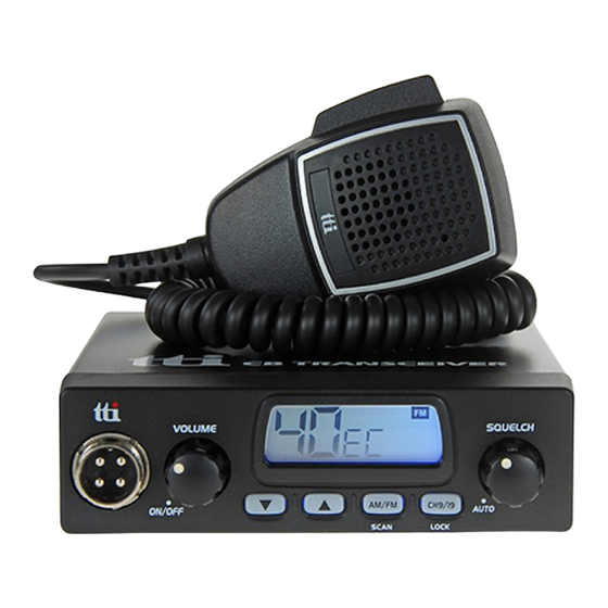
- Page 3 SECTION1 SPECIFICATIONS Channel 40 (See the frequency band chart) Frequency Range 26.56 MHz ~ 28.00 MHz Operating mode F3E (FM), A3E (AM) Frequency Control PLL Synthersizer Frequency Tolerance 0.002% Operating Temperature Range -10 to + 55 C Microphone Plug-in Type Input Voltage 13.2V DC ±...
- Page 4 SECTION2 CIRCUIT DESCRIPTION ------------ Contents ------------- General 1-1. Receiver 1.2. Transmitter Technical Description 2-1. General 2-2. Type of emission 2-3. Frequency Table 2-4. RF Power Output 2-5. DC input Voltage and Current with 13.2V DC Input to Power AMP 2-6. Receiver IF and Local Oscillator Frequencies Semiconductors and Function Description of Frequency Determining and Stabilizing Circuit...
- Page 5 General 1-1. Receiver Display : 40 Channels and other functions indication Frequency Range : 26.965 to 27.405 [MHz] Frequency Response : 300 to 2,500 [Hz] Power Source : 13.2 [V] DC Audio Output Load : 8 [OHM] Resistive Audio Output : 4.0 [W] (or More) Squelch : Adjustable from 0.2[uV] to 1 [mV] Sensitivity : FM : 20 dB [SINAD] under 1.0 [uV] or less...
- Page 6 Technical Description 2-1. General Model CB-550 is an mobile type AM/FM radio transceiver for use of the Citizen Radio Service. Front Panel Controls LCD Display(Cannel ,RX,TX,AQ,SCAN,AM,FM,EMG Indicator). Receiver Audio Control (With Power ON/OFF Control) Volume Squelch Control Volume (S/W ON : TIGHT, S/W OFF : AUTO SQ) RF Gain Control Volume CHANNEL UP/DOWN TACT SWITCH.
- Page 7 2-3. SEMICONDUCTORS AND FUNCTION REF.NO DESCRIPTION REMARK KTC4080E RF AMP KTC4080E 1'st MIXER KTC4080E 1'st MIXER KTC4075E RF ATTENUATOR RF ATTENUATOR KTC4080E IF AMP KTC4080E IF AMP KRA2014E A.N.L. KRC410E SQ MUTE KTC4075E RF ARRENUATOR RF ATTENUATOR KRC402E AUTO SQ S/W QAS1 KRC410E FM MUTE...
- Page 8 Description of Frequency Determining and Stabilizing Circuitry 4-1. Introduction The Frequencies for transmitter and receiver first local frequencies are all derived from a signal 10.695MHz cry stal and second local frequencies are derived from 10.240 MHz crystal by means of a Phase lcoked loop.
- Page 9 Transmit CH 1 , 13.4825 MHz 26.965 MHz Transmit CH 40 , 13.7025 MHz 27.405 MHz Since all frequencies are obtained from the crystal controlled PLL oscillator, all outputs are coherent with the crystal oscillator frequency and matching the same percentage accuracy.
- Page 10 Program Data & Frequency[Table 1] Frequency Channel [MHz] Fvco Fvco 26.965 3254 16.27 5393 13.4825 26.975 3256 16.28 13.4875 5395 26.985 3258 16.29 13.4925 5397 27.005 3262 16.31 13.5025 5401 27.015 3264 16.32 13.5075 5403 27.025 3266 16.33 13.5125 5405 27.035 3268 16.34...
- Page 11 4-3. Description Of Each Block 4-3-1. Introduction The synthesizer is implemented with the following companents : PLL IC (IC6) X-TAL(X2) VARICAP DIODE(DV1,2) IC6 is a CMOS LSI that includes most of PLL block. The VCO with varicap diode DV1,2 as a part of the oscillator tank circuit.
- Page 12 4-3-6. Transmitter / Receiver Buffer AMP The VCO output is fed into buffer AMP QW1 from the capacitor of CW1. 4-3-7. Transmitter Doubler The output signal of QW1 goes to an amplifier tuning circuit(27MHz) QW2, LT1, LT2 which doubles incoming 13MHz signals. 4-3-8.
- Page 13 The output of doubler AMP QW2 is fed through double tuning(27MHz) LT1 and LT2 to the base of PRE AMP QT2. The output is then supplied through tuning circuit LT3 to RF driver AMP QT3. The QT3 output is capacitance divided by tuning circuit CT10, CT12, LT4, CT13 and passed through the base of final RF stage QT4.
- Page 14 AM signals form the PIN 5 of IC1 were tapped with CR34 and amplified two-stage amplifier QR5,6 is a a first 455KHz amplifier. DR3 is a detector diode witch produce audio signal as well as negative DC voltage fir AGC action. The negative voltage laso provides forward biasing to the mitter of ANL clipping TR QR7.
- Page 15 5-2. Transmitter Section Alignment 5-2-1. Required Test Equipment : If uses in HP8920, the 1)~7) equipment is not a necessity. 1) RF Power Meter 6) Frequency counter 2) 50 ohm Load (non-inductive) DC Voltmeter 8) Spectrum analyzer 3) RF attenuator (30dB) 4) Audio Generator 9) DC power supply: 13.8VDC / 3A 5) Modulation meter...
- Page 16 Alignment Step Test Item UUT setting Equipment setting Spec. point Channel: CH19 Connect the equipment and Deviation Function: UUT as shown on Figure.3 Adjustment 1) FM mode Audio generator 2) CB 1) Set to 1KHz / 50mV 2) Input to MIC 1.8KHz Unit: TX condition (PTT on)
- Page 17 Figure 2 Figure 3 30dB ATT Spectrum Notch filter T CB550 Power Supply Figure 4 5-3. Receiv er Section Alignment 5-3-1. Re quired Test Equipment : If uses in HP8920, the 1)~4) equipment is not a necessity. 1) Standard Signal Generator (SSG) 5) Oscilloscope 2) SINAD Meter 6) DC power supply (13.2V/3A)
- Page 18 Alignment Step Test Item UUT setting Equipment setting Spec. point RX sensitivity Same as step ”1” SSG setting: <-107dBM 1) RF level: -107dBm at 10dB SINAD 2) Others: same as step ”1” (if not,align again) Channel: CH19 Connect the equipment and Audio Level: Audio output Function:...
- Page 19 SECTION3 PART LIST LEVEL DESCRIPTION ASSY 5A0-5504-000 LCD PCB ASS¡Ç Y - TCB550 1.00 PART 102-331J-S00 FILM RES. 330OHM 0.5W +-5 ST 1.00 PART 102-471J-S00 FILM RES. 470OHM 0.5W +-5 ST 1.00 PART 142-100J-000 CHIP RES. 0603 10OHM +-5 PHILIPS 1.00 PART 142-102J-000...
- Page 20 PART 500-5504-000 LCD PCB MP03 - TCB550 1.00 PART 564-1109-100 SWITCH TACT KFC-821 GABOU 4.00 PART 701-C7700-60A DIFFUSER LENS ACRYL CLEAR 1.00 PART 701-C7700-70A REFLECTOR ACRYL CLEAR 1.00 PART 702-C7700-50A LCD BRACKET SPTE 0.3T DESHAN 1.00 PART 703-C7700-20A ZEBRA SILICONE 1.00 PART 718-R000D-036...
- Page 21 PART 142-222J-000 CHIP RES. 0603 2.2KOHM +-5 PHILIPS 7.00 PART 142-223J-000 CHIP RES. 0603 22KOHM +-5 PHILIPS 5.00 PART 142-224J-000 CHIP RES. 0603 220KOHM +-5 PHILIPS 1.00 PART 142-225J-000 CHIP RES. 0603 2.2MOHM +-5 PHILIPS 1.00 PART 142-229J-000 CHIP RES. 0603 2.2OHM +-5 PHILIPS 3.00 PART 142-272J-000...
- Page 22 PART 202-2279-M00 ELECT CAP. 220UF KR1-16V221MB 5x11 DONGXIANG 1.00 PART 202-4749-M00 ELECT CAP. 0.47UF KR1-16V47MA 5x11 DONGXIANG 1.00 PART 202-4769-M00 ELECT CAP. 47UF KR1-16V470MA 5x11 DONGXIANG 2.00 PART 202-4779-M00 ELECT CAP. 470UF KR1-25V471MA 10x15 DONGXIANG 1.00 PART 212-050C-6C0 CHIP CERAMIC CAP. 0603 5PF NP0 50V +-0.25 PHILIPS 1.00 PART 212-080C-6C0...
- Page 23 PART 22D-331C-J00 DISK CAP.CC1HSL331J (Label 50VSL331J) SAMIL 1.00 PART 22D-471C-J00 DISK CAP.CC1HSL471J (Label 50VSL471J) SAMIL 1.00 PART 22D-561C-J00 DISK CAP.CC1HSL561J (Label 50VSL561J) SAMIL 1.00 PART 22D-681C-J00 DISK CAP. CC1HSL681J (Label 50VSL681J) SAMIL 1.00 PART 230-2000-000 DIP TRIMMER CAP. 6DIA 20PF KCVN620 FOKITS 1.00 PART 300-1504-000...
- Page 24 PART 342-0120-B00 CHIP DIODE SWITCHING KDS120E KEC 1.00 PART 342-0121-B00 CHIP DIODE SWITCHING KDS121E KEC 3.00 PART 342-0122-A00 CHIP DIODE SWITCHING KDS122 KEC 1.00 PART 342-5822-001 DIP SCHOTTKY DIODE 1N5822 GD 1.00 PART 343-1060-000 DIODE 1N60 1.00 PART 343-4004-000 DIODE 1N4004TR 400V 1A 1.00 PART 343-5402-000...
- Page 25 PART 427-0017-000 CORE SPRING 5.5TX0.45XM5ERX2.3 0.17UH FINE 3.00 PART 500-5504-100 MAIN PCB MP01 - TCB550 1.00 PART 535-3500-100 JACK DC PJ-625 GABOU 1.00 PART 540-0218-000 WAFER 2PIN PH-2A 180C FINE 1.00 PART 570-1001-000 VR R16100NS-KA20D11.5-B103-000-G74 CTR 1.00 PART 570-5001-000 VR R16100NS-KA20D11.5-A503-000-G74 CTR 1.00 PART 702-C5500-50A...
- Page 26 PART 708-26082-BPH SCREW TAP(+) 2.6X8L-2S BLACK PH(HEAD DIA 4.2) 2.00 PART 712-M70NI-001 RING NUT BsBm 2.00 PART 719-S000D-035 DOUBLE TAPE(WINDOW) 3M 0.16t 1.00 ASSY 700-C550M-B00 MAIN BODY ASSY - TCB550 1.00 PART 541-0239-002 CONNECTOR FD-ANT-1 NINGBO 1.00 PART 543-2000-000 1.00 POWER CORD ASS¡Ç...
- Page 27 WARNING LABEL 1.00 PART 834-0002-000 ROHS STICKER - TTI 0.10 PART 836-C550-000 LCD PROTECTIVE SHEET 1.00 PART 837-0001-000 OPP TAPE 50MM TTI LOGO 0.29 PART 838-0001-000 YELLOW STRAP 0.26 PART 83A-0001-000 SILICA GEL 1g 1.00 PART 905-C550-000 MICROPHONE ASSY - TCB550...
- Page 28 SECTION4 MECHANICAL DISASSEMBLY...
- Page 30 SECTION5 BOARD LAYOUT Main PCB (Top side)
- Page 31 Main PCB (Bottom side)
- Page 32 5-2 Front PCB (Top side)
- Page 33 Front PCB (Bottom side)
- Page 34 5-3 LED PCB (Top side)
- Page 35 LED PCB (Bottom side)
- Page 36 5-4 Volume PCB...
- Page 37 5-5 MIC PCB...
- Page 38 SECTION6 BLOCK DIAGRAM...
- Page 39 SECTION7 SCHEMATIC...
Need help?
Do you have a question about the TCB-550 and is the answer not in the manual?
Questions and answers