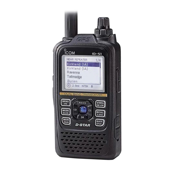
Icom ID-51E User Manual
Vhf/uhf transceivers
Hide thumbs
Also See for ID-51E:
- Advanced manual (413 pages) ,
- Advanced instructions (369 pages) ,
- Basic instructions (104 pages)
Table of Contents
Advertisement
Quick Links
Advertisement
Table of Contents

Subscribe to Our Youtube Channel
Related Manuals for Icom ID-51E


Summary of Contents for Icom ID-51E
- Page 1 VHF/UHF TRANSCEIVER S-14914XZ-C1 March 2013...
- Page 2 8. READ the instructions of the test equipment thoroughly before connecting it to the transceiver. Icom, Icom Inc. and the Icom logo are registered trademarks of Icom Incorporated (Japan) in Japan, the United States, the United Kingdom, Germany, France, Spain, Russia and/or other countries.
-
Page 3: Table Of Contents
TABLE OF CONTENTS SECTION SPECIFICATIONS SECTION INSIDE VIEWS SECTION DISASSEMBLY INSTRUCTION SECTION CIRCUIT DESCRIPITON RECEIVER CIRCUITS ....................4-1 TRANSMITTER CIRCUITS ..................4-2 FREQUENCY SYNTHESIZER CIRCUITS ..............4-4 VOLTAGE BLOCK DIAGRAM ..................4-4 PORT ALLOCATIONS ....................4-5 SECTION ADJUSTMENT PROCEDURES PREPARATION ......................5-1 FREQUENCY ADJUSTMENT .................. -
Page 4: Specifications
Internal speaker • Power supply : 10.0–16.0 V DC for external DC : More than 0.2 W with a 8 Ω load External speaker power, or specifi ed Icom’s battery • Selectivity pack : More than 55 dB (Wide) • Digital transmission speed : 4.8 kbps... -
Page 5: Section 2 Inside Views
SECTION 2. INSIDE VIEWS • LOGIC UNIT EEPROM (IC3) LEVEL CONVERTER (IC21) DSP FLASH MEMORY (IC20) MIC MUTE SW (IC16) EEPROM (IC7) MODE SW (IC390) AF FILTER (IC350) (IC5) AF AMP (IC2) AF AMP (IC300) CLOCK OSCILLATOR (For the CPU) TONE FILTER (X2) (Q330) - Page 6 • MAIN UNIT (TOP VIEW) POWER AMP (Q45) APC AMP (IC14) CURRENT DETECTOR 3VS LINE REGULATOR (IC5) (IC12) VCC LINE SW (Q907) (Q8) (Q906) VCC LINE SW RF AMP (Q2) (Q780) D/A CONVERTER (IC952) LOCK VOLTAGE BUFFER (Q451) PLL IC (Band B) (IC450) +5 V REGULATOR (IC15)
- Page 7 • MAIN UNIT (BOTTOM VIEW) DRIVE AMP (Q41) VHF RF AMP (Band A/B) (Q702) UHF RF AMP (Band A/B) (Q602) VHF RF AMP (Band A) (Q701) UHF RF AMP (Band A) (Q601) UHF RF AMP (Band B) (Q641) 1ST IF FILTER (Band A) (FI3) VHF RF AMP (Band B) (Q740)
-
Page 8: Section 3 Disassembly Instruction
1) Remove 2 dials and antenna nut from the front panel. 5) Unsolder 6 points at the rotary encoder. Inner dial UNSOLDER Screws x5 Antenna nut Outer dial Remove with; “ICOM Driver (Q)” Solder (8960000370) remover LOGIC UNIT 2) Remove 2 screws from the bottom of chassis. Screws Rotary encoder 6) Separate the LOGIC UNIT from the chassis, and then disconnect the fl... - Page 9 2. REMOVING THE MAIN UNIT 3) Unsolder a point at the antenna connector. 1) Unsolder 2 points on the shield plate. UNSOLDER UNSOLDER Solder remover Solder remover Shield plate 4) Remove 6 screws from the MAIN UNIT, and then 2) Remove 5 screws from the shield plate, and then remove the MAIN UNIT from the chassis.
-
Page 10: Circuit Description
SECTION 4. CIRCUIT DESCRIPTION UHF BAND (380–479 MHz) 4-1 RECEIVE CIRCUITS The RF signal from the antenna is passed through the HPF RF CIRCUITS (L512, L514, C545, C548, C550, C551 and C554), two LPFs VHF BAND (108–174 MHz) (L511, C536, C539 and L507, C524, C526, C529), ANT SW The RF signal from the antenna is passed through two LPFs (D508 and D510) and BPF (L608, L610, L612, C630, C631 (L513, L515, L516, C547, C549, C553, C555 and C556),... - Page 11 1ST IF CIRCUITS UHF BAND (380–479 MHz) VHF BAND (108–174 MHz) • Band A • Band A (137–174 MHz) The RX signal from the RF circuit is applied to the 1st mixer The RX signal from the RF circuit is applied to the 1st mixer (Q801) and mixed with the 1st LO signal, resulting in the 46.35 (Q820) and mixed with the 1st LO signal, resulting in the 46.35 MHz 1st IF signal.
- Page 12 2ND IF CIRCUITS • Band B • Band A The 1st IF signal from the 1st IF circuit is applied to the IF IC The 1st IF signal from the 1st IF circuit is applied to the IF IC (IC901, pin 16), which contains the 2nd IF AMP, 2nd mixer, (IC13, pin 16), which contains the 2nd IF AMP, 2nd mixer, FM FM demodulator, and so on.
- Page 13 DIGITAL DEMODULATION CIRCUIT (LOGIC UNIT) RADIO RECEIVE CIRCUITS While operating in the DV mode, the demodulated signal • FM BAND (76–108 MHz) (digital audio signal) is passed through the LPF (R305, R336, The RF signal from the antenna or earphone is passed through R339, C334 and C337) and amplifi...
-
Page 14: Transmitter Circuits
MODULATION CIRCUITS (MAIN UNIT) 4-2 TRANSMIT CIRCUITS The MIC signal from the TX AF circuits is applied to the VHF TX AF CIRCUIT (LOGIC UNIT) VCO (Q311, D304–D306) or UHF VCO (Q27, D10–D12) as The AF signal from the internal or external microphone (MIC a modulation signal. - Page 15 TX AMP CIRCUITS (MAIN UNIT) APC CIRCUITS (MAIN UNIT) The TX signal is passed through the buffer (Q48) and ATT The voltage produced at the LPFs (VHF band; L513, L515, (D20, D21), which controls the TX output power by the APC L516, C547, C549, C553,C555 and C556, UHF band;...
-
Page 16: Frequency Synthesizer Circuits
UHF VCO (VCO1 UNIT) 4-3 FREQUENCY SYNTHESIZER CIRCUIT The UHF VCO (Q27, D10–D12) generates 1st LO signal (MAIN UNIT) (for receiving a UHF signal on band B). The output of buffer VCOs (Q200) is amplifi ed by the LO AMP (Q201), and then used as The ID-51A/E has total of four VCOs;... -
Page 17: Port Allocations
4-4 PORT ALLOCATIONS • CPU (LOGIC UNIT: IC5) Line Name Description Line Name Description VOX sensing voltage. DICK1 [DIAL] (outer dial) (S12) phase-A TSQL/DTCS tone signal. (Band PLL unlock detection. (Band A) ACTCIN AUNLK L=Unlocked. CLSFT2** Clock frequency shift control. DALD D/A converter serial strobe. - Page 18 • CPU (LOGIC UNIT: IC5) (continued) Line Name Description Line Name Description IOEN Expander chip enable. EEPROM serial clock. DSP clock shift control. microSD card insert detection. DCSFT SD_SENC L=+600 Hz shifted. L=Inserted. BPLLSTB PLL serial strobe. (Band B) Serial data to the attached mi- SD_TXD croSD card.
-
Page 19: Preparation
SECTION 5. ADJUSTMENT PROCEDURE 5-1 PREPARATION ¤ REQUIRED EQUIPMENTS EQUIPMENT GRADE AND RANGE EQUIPMENT GRADE AND RANGE Voltage range : 1–15 V Modifi ed 3-conductor plugs Power supply JIG cables Current capacity : More than 3 A (See the illustration below) Audio generator Frequency range : 300–3000 Hz... - Page 20 • ENTERING THE ADJUSTMENT MODE 1) Connect the JIG cable “#1” to [SP]. (See page 5-1) 2) While holding down [SQL] and , turn ON the power. [SQL] Connect the JIG cable “#1” (See page 5-1) here. Push to turn ON the power. [QUICK/MENU] •...
-
Page 21: Frequency Adjustment
5-2 FREQUENCY ADJUSTMENT Select an adjustment item using , and then set the adjustment value as specifi ed using [DIAL]. ADJUSTMENT ADJUSTMENT OPERATION VALUE ITEM REFERENCE 1) Set the power supply voltage to 7.4 V. FREQUENCY 2) Connect a power meter or dummy load to the antenna connec- Displayed tor. - Page 22 5-3 TRANSMIT ADJUSTMENT (Continued) • IDLING CURRENT ADJUSTMENT (at 7.4 V) Select an adjustment item using , and then set the adjustment value as specifi ed using [DIAL]. ADJUSTMENT ADJUSTMENT OPERATION VALUE ITEM DRIVE AMP 1 1) Set the power supply voltage to 7.4 V. IDLING CURRENT 2) Connect an RF power meter to the antenna connector.
- Page 23 5-3 TRANSMIT ADJUSTMENT (Continued) • IDLING CURRENT ADJUSTMENT (at 13.5 V) Select an adjustment item using , and then set the adjustment value as specifi ed using [DIAL]. ADJUSTMENT ADJUSTMENT OPERATION VALUE ITEM DRIVE AMP 1 1) Set the power supply voltage to 13.5 V. (supplying from [DC IN]) IDLING CURRENT 2) Connect an RF power meter to the antenna connector.
- Page 24 5-3 TRANSMIT ADJUSTMENT (Continued) • TRANSMIT POWER ADJUSTMENT (at 5.5 V) Select an adjustment item using , and then set the adjustment value as specifi ed using [DIAL]. ADJUSTMENT ADJUSTMENT OPERATION VALUE ITEM TRANSMIT 1 1) Set the power supply voltage to 5.5 V. POWER 2) Connect an RF power meter to the antenna connector.
- Page 25 5-3 TRANSMIT ADJUSTMENT (Continued) • TRANSMIT POWER ADJUSTMENT (at 13.5 V) Select an adjustment item using , and then set the adjustment value as specifi ed using [DIAL]. ADJUSTMENT ADJUSTMENT OPERATION VALUE ITEM TRANSMIT POWER 1 1) Set the power supply voltage to 13.5 V. (supplying from [DC IN]) –...
- Page 26 5-3 TRANSMIT ADJUSTMENT (Continued) • DEVIATION ADJUSTMENTS Select an adjustment item using , and then set the adjustment value as specifi ed using [DIAL]. ADJUSTMENT ADJUSTMENT OPERATION VALUE ITEM FM DEVIATION 1 1) Set the power supply voltage to 7.4 V. 2) Connect a modulation analyzer to the antenna connector through an attenuator, and set it as;...
- Page 27 5-3 TRANSMIT ADJUSTMENT (Continued) • DEVIATION ADJUSTMENTS (Continued) Select an adjustment item using , and then set the adjustment value as specifi ed using [DIAL]. ADJUSTMENT ADJUSTMENT OPERATION VALUE ITEM DV BALANCE 1 1) Set the power supply voltage to 7.4 V. 2) Connect a modulation analyzer to the antenna connector through an attenuator, and then set it as;...
- Page 28 5-3 TRANSMIT ADJUSTMENT (Continued) • TONE DEVIATION ADJUSTMENTS Select an adjustment item using , and then set the adjustment value as specifi ed using [DIAL]. ADJUSTMENT ADJUSTMENT OPERATION VALUE ITEM TONE DEVIATION 1 1) Set the power supply voltage to 7.4 V. 2) Connect a modulation analyzer to the antenna connector through an attenuator, and then set it as;...
-
Page 29: Receive Adjustment
5-3 TRANSMIT ADJUSTMENT (Continued) 5-4 RECEIVE ADJUSTMENTS 1) Select an adjustment item (band) using 2) Set the SSG as specifi ed (frequency, deviation and output level), and then push to automatically adjust. ADJUSTMENT ADJUSTMENT OPERATION VALUE ITEM RECEIVE NOTE: “RECEIVE SENSITIVITY” must be adjusted before “S-METER.” Otherwise, “S-METER” will SENSITIVITY not be adjusted properly. - Page 30 5-3 TRANSMIT ADJUSTMENT (Continued) 5-4 RECEIVE ADJUSTMENTS (Continued) 1) Select an adjustment item (band) using 2) Set the SSG as specifi ed (frequency, deviation and output level), and then push to automatically adjust. ADJUSTMENT ADJUSTMENT OPERATION VALUE ITEM S-METER NOTE: “RECEIVE SENSITIVITY” must be adjusted before “S-METER” and “S-METER S3 LEVEL.” Other- [A-BAND] wise, “S-METER”...
- Page 31 5-3 TRANSMIT ADJUSTMENT (Continued) 5-4 RECEIVE ADJUSTMENTS (Continued) 1) Select an adjustment item (band) using 2) Set the SSG as specifi ed (frequency, deviation and output level), and then push to automatically adjust. ADJUSTMENT ADJUSTMENT OPERATION VALUE ITEM SQUELCH 1 1) Set the power supply voltage to 7.4 V. –...
-
Page 32: Parts List
SECTION 6. PARTS LIST [MAIN UNIT] [MAIN UNIT] PARTS PARTS DESCRIPTION DESCRIPTION LOCATION LOCATION 1110007610 S.IC TPA0211DGNR 89.2/30.7 D502 1750002580 S.DIO HVU187TRF-E 10.4/19.9 1180004210 S.REG XC6221A402NR-G 49.3/20.6 D503 1750001910 S.DIO HVD144AKRF-E 5.9/22.1 6910022360 S.DC TPS62110RSAR 84.0/12.7 D504 1750001910 S.DIO HVD144AKRF-E 4.8/22.1 1110006380 S.IC LM2904PWR... - Page 33 [MAIN UNIT] [MAIN UNIT] PARTS PARTS DESCRIPTION DESCRIPTION LOCATION LOCATION L603 6200009070 S.COI LQW18AN18NG00D R110 7030005290 S.RES ERJ2GEJ 682 X (6.8K) 56.1/40.2 (LQW1608A18NG00) 44.8/21.9 R112 7030008270 S.RES RR0510P-104-D (100K) 51.4/41.2 L604 6200011580 S.COI LQW18AN33NG00D 39.7/21.5 R113 7030005210 S.RES ERJ2GEJ 822 X (8.2K) 54.7/39.0 L605 6200011590 S.COI...
- Page 34 [MAIN UNIT] [MAIN UNIT] PARTS PARTS DESCRIPTION DESCRIPTION LOCATION LOCATION R462 7030010040 S.RES ERJ2GEJ-JPW 79.1/34.6 R832 7030008280 S.RES ERJ2GEJ 271 X (270) 60.9/17.4 R465 7030010040 S.RES ERJ2GEJ-JPW 80.1/29.2 R833 7030005080 S.RES ERJ2GEJ 823 X (82K) 55.3/19.6 R466 7030010040 S.RES ERJ2GEJ-JPW 87.8/36.5 R834 7030008270 S.RES RR0510P-104-D (100K)
- Page 35 [MAIN UNIT] [MAIN UNIT] PARTS PARTS DESCRIPTION DESCRIPTION LOCATION LOCATION 4030017460 S.CER C1005 JB 1H 102K-T 22.5/20.7 C259 4030017640 S.CER C1005 CH 1H 150J-T 51.1/30.5 4030017640 S.CER C1005 CH 1H 150J-T 81.5/20.1 C263 4030016790 S.CER C1005 JB 1E 103K-T 43.2/34.6 4030017460 S.CER C1005 JB 1H 102K-T 49.0/31.9 C264...
- Page 36 [MAIN UNIT] [MAIN UNIT] PARTS PARTS DESCRIPTION DESCRIPTION LOCATION LOCATION C510 4030017590 S.CER C1005 CH 1H 070C-T [EUR] T 12.3/22.6 C716 4030017350 S.CER C1005 CH 1H 020B-T 29.9/11.2 4030017590 S.CER C1005 CH 1H 070C-T [UK] C717 4030017690 S.CER C1005 CH 1H 121J-T 32.2/9.8 4030017590 S.CER C1005 CH 1H 070C-T [ITR]...
- Page 37 [MAIN UNIT] [MAIN UNIT] PARTS PARTS DESCRIPTION DESCRIPTION LOCATION LOCATION C921 4030017040 S.CER C1005 JB 1A 333K-T 71.5/5.6 EP782 6910023920 S.BEA BLM15GA750SN1D 84.4/39.7 C922 4030017460 S.CER C1005 JB 1H 102K-T 71.5/6.5 EP783 6910023920 S.BEA BLM15GA750SN1D 83.2/38.4 C923 4030017670 S.CER C1005 CH 1H 390J-T 74.5/6.1 EP784 6910014690 S.BEA...
- Page 38 [VCO1 UNIT] [VCO1 UNIT] PARTS PARTS DESCRIPTION DESCRIPTION LOCATION LOCATION 1590004070 S.TRA LDTC144EET1G <SLVJ> 7.5/1.3 C374 4030017460 S.CER C1005 JB 1H 102K-T 11.5/16.0 1530003260 S.TRA 2SC5006-T1 16.6/5.4 C375 4030007060 S.CER C1608 CH 1H 270J-T 17.0/13.5 Q200 1530003260 S.TRA 2SC5006-T1 16.4/8.9 C376 4030007080 S.CER C1608 CH 1H 390J-T 17.0/12.3...
- Page 39 [VCO2 UNIT] [VCO2 UNIT] PARTS PARTS DESCRIPTION DESCRIPTION LOCATION LOCATION 1590004070 S.TRA LDTC144EET1G <SLVJ> 7.5/1.3 C374 4030017460 S.CER C1005 JB 1H 102K-T 11.5/16.0 1530003260 S.TRA 2SC5006-T1 16.6/5.4 C375 4030007060 S.CER C1608 CH 1H 270J-T 17.0/13.5 Q200 1530003260 S.TRA 2SC5006-T1 16.4/8.9 C376 4030007080 S.CER C1608 CH 1H 390J-T 17.0/12.3...
-
Page 40: Logic Unit
[LOGIC UNIT] [LOGIC UNIT] PARTS PARTS DESCRIPTION DESCRIPTION LOCATION LOCATION 1120003020 S.IC MAX3221IPWR 53.0/45.2 1750002540 S.DIO LRB520G-30T1G <SLVJ> 39.4/16.1 1140015870 S.IC M24M01-RMN6TP 6.4/32.5 1790001960 S.VAR VC060303A100RP 44.3/40.0 1130015740 S.IC S-35390A-I8T1G 92.2/12.7 D180 1750001810 S.DIO L1SS400T1G <SLVJ> 29.5/36.5 1140016250 S.IC R5F56107WNBG 49.2/12.6 D181 1750001810 S.DIO... - Page 41 [LOGIC UNIT] [LOGIC UNIT] PARTS PARTS DESCRIPTION DESCRIPTION LOCATION LOCATION R102 7030005240 S.RES ERJ2GEJ 473 X (47K) 67.0/37.7 R246 7030005090 S.RES ERJ2GEJ 104 X (100K) 15.5/15.8 R103 7030005050 S.RES ERJ2GEJ 103 X (10K) 63.9/37.3 R247 7030005090 S.RES ERJ2GEJ 104 X (100K) 18.7/27.9 R104 7030008010 S.RES ERJ2GEJ 123 X (12K)
- Page 42 [LOGIC UNIT] [LOGIC UNIT] PARTS PARTS DESCRIPTION DESCRIPTION LOCATION LOCATION R410 7030005090 S.RES ERJ2GEJ 104 X (100K) 41.6/14.7 C132 4030016930 S.CER C1005 JB 1A 104K-T 27.1/41.5 R411 7030005090 S.RES ERJ2GEJ 104 X (100K) 47.1/5.1 C134 4030016930 S.CER C1005 JB 1A 104K-T 21.7/7.0 R412 7030005090 S.RES ERJ2GEJ 104 X (100K)
- Page 43 [LOGIC UNIT] [LOGIC UNIT] PARTS PARTS DESCRIPTION DESCRIPTION LOCATION LOCATION C356 4030018090 S.CER C1005 JB 1E 822K-T 52.8/26.3 6910023920 S.BEA BLM15GA750SN1D 75.3/47.5 C357 4030017790 S.CER C1005 JB 1H 682K-T 51.0/28.1 6910023920 S.BEA BLM15GA750SN1D 61.1/44.1 C358 4030016930 S.CER C1005 JB 1A 104K-T 53.8/28.1 6910023920 S.BEA BLM15GA750SN1D...
- Page 44 SECTION 7. MECHANICAL PARTS [CHASSIS PARTS] [MAIN UNIT] ORDER ORDER DESCRIPTION QTY. DESCRIPTION QTY. 6450000870 HEC2711-01-020 6910015630 2682 ANT CONNECTOR <EIK> 6510028130 AXK5S50047YG 6510025880 TC38-108-01 <CFE> 2510001650 K028NA510-13 <OSC> 6450000131 HSJ1102-018540 J450* 6510029520 AXK5F12347YG 8900014801 OPC-1573-1 (P0.5N10L50) J451* 6510029520 AXK5F12347YG 6910023940 PGS4ER-CX-512 2260001900 SW-149 (SKHLLD) 8010022510 3390 CHASSIS...
- Page 45 [ACCESSORIES] MP33(C) EP1(C) MP14(C) GPS module MP29(C) J1(C) MP25(C) W1(C) MP27(C) MP3(C) MP1(C) (Bottom view) MP24(C) S12(L) MP8(C) MP49(C) MP15(C) MP23(C) MP1(M) MP34(C)×2 MP13(C) MP35(C)×5 MP61(C) MAIN UNIT MP51(C) MP52(C) MP50(C) MP60(C) MP59(C) MP53(C) MP43(C) VCO2 UNIT MP48(C) MP42(C) MP31(C) MP35(C)×5 MP1(V2) MP46(C)
- Page 46 The combination of top side and bottom side of this SECTION 9. BOARD LAYOUTS • LOGIC UNIT (TOP VIEW) DS12 C394 R391 Q390 R395 R396 LCDCS LCDRES LCDRS LCDCK LCDDT DS11 DS10 R398 R397 C399 C517 C398...
- Page 47 The combination of top side and bottom side of this • LOGIC UNIT (BOTTOM VIEW) [PWR] R419 R119 R237 C103 R112 R198 R118 R239 R242 R113 C107 C171 R227 R109 C311 R108 C132 IC20 R217 C102 R222 [DIAL] R314 C305 R308 R181 R418...
- Page 48 The combination of top side and bottom side of this • MAIN UNIT [MIC] [SP] [DC IN] (TOP VIEW) IC15 R169 C177 C136 C194 R171 IC12 C198 R112 C989 EP13 EP15 R110 C210 C102 C230 C110 R113 C237 C991 C468 R203 R183 R466...
- Page 49 The combination of top side and bottom side of this • MAIN UNIT (BOTTOM VIEW) C221 EP12 EP784 R192 C224 R201 EP11 C220 C796 C797 EP10 EP785 EP782 R273 MP12 C446 MP13 C448 C445 R200 R170 R209 EP23 C977 C235 D820 C200 R820...
- Page 50 SECTION 10. BLOCK DIAGRAM EARANT BTL4.2V BTL4.2V FMPTX RADIO BUFF IC20 AFON CLONE IC25 IC25 D_AS MAIN UNIT DTCS EXTMIC IC25 VCOMOD CHASSIS UNIT MMUTE LINEAR MODE REFMOD CTCOUT CODEC DMOD IC25 IC16 IC390,Q390 AUSTB MMUTE PLAY SC_CLK SC_SDI SC_SDO IC25 SC_LR DAFO...
- Page 51 D502,Q504,D511 TEMP VCO_A ANTENNA VCC-I VVCO3(VAV3) VCOMOD D501 TX:400.000M~479.000MHz D508 D510 RX:380.000M~479.000MHz AVCO_SHIFT SHIFT A_LOOUT DRIVE BUFF BUFF Q308 Q200 Q201 3VS,+5V D308 Q311,D304,D305,D306 D20,D21 UVCO3(UAV3) D505,D509 LOOP AUNLK VCOMOD IC12 IC14A REFMOD GATE GATE ANT SW Q501 CTRL CTRL CTRL CTRL Q502...
- Page 52 SECTION 11. VOLTAGE DIAGRAM • LOGIC UNIT (1/3) G_VDD 1.82V J271 DR_I2C_DIO DR_I2C_CLK 3.30V TIMEMARK 3.30V IC12 R105 G_HIB IC13 VOUT 4.73V LDTC144EE BLED 0.0039 IC21 SRESET VOUT R101 XC6221A332MR 100k LDTC144EE XC6221A332NR 2SA1832 L1SS400 CL-165HR 2SC4738 LDTC144EE SN74AUP1T17DCKR Q380 INT1 3.29V TEMP...
- Page 53 • LOGIC UNIT (2/3) BLM18RK102SN1 R156 3.3V_VDD EP12 DVDD_3.3V SC_LR MMZ1005S601CT 3.28V BSP_FSX 3.28V SC_CLK BSP_CLKX SC_SDO BSP_DX BLM18RK102SN1 NFM18PC104R1C3 SC_SDI EP10 C129 CP06S CP48 CP06S CP49 R284 CP52 CP06S C110 R121 R178 CLONE 270k 330k R416 IC10 AD_CS R114 R281 CVDD_1.3V ADJ2...
- Page 54 • LOGIC UNIT (3/3) R310 TX A DV:3.28V Other:0V Q300 Q302 LDTC144EE LDTC144EE R314 C311 D_AS 0.039 ADET ADET BDET BDET R312 R318 ATONE AADIN AADIN AADIN IC300 C340 10k R339 R336 R305 R307 ADET 150k 0.33 R320 C315 C300 C306 AAFFILIN 3.3k...
- Page 55 • MAIN UNIT (1/3) VCO1 UNIT J450 A_LOOUT OSCI 3.31V OSCO EP40 APPS A_LV MMZ1005Y102CT 1.5k 1.2k 1.2k APLLSTB R103 R113 CR-875 XFIN 8.2k 0.001 0.001 MB15E03SLPFV1 VCON 2SK880 R112 560k 100k 1.46V Q470 Q471 VCO2 UNIT J451 IC450 B_LOOUT R450 DMA561050 DMA561050...
- Page 56 • MAIN UNIT (2/3) TTEMP TX VHF:4.00V RX:0V(TX UHF) R501 Q504 EP16 DRC9114T0L MPZ1608S101A VCC-I NTCG10 Q37 2SA1832 C242 R507 R512 7.38V C251 C527 MMZ2012Y102B 0.001 0.001 TX 4.53V TX VHF:1.60V TX UHF:3.55V R176 AVR-M1005C270M C216 20.0N J501 R163 0.001 2600 ANT CONNECTOR T3C_INV *C507...
- Page 57 • MAIN UNIT (3/3) ANOIS ARSSI ADET CHGC 3.31V CHGH TXI-V 4.76V 4.18V IOEN BTVIN IC17 ASQLIN IOSTB1 (Radio RF) ASQLOUT DASTB1 VOUT BSQLOUT BTDETO BRSSI BPLLSTB EP21 BNOIS R142 XC6222D421MR VCOMOD N010M9 1.63V BDETO AUNLK 100k EP22 IC16 BSQLIN APLLSTB VIN6 VIN3...
- Page 58 • VCO1 UNIT • VCO2 UNIT PLLOUT L203 LOOUT PLLOUT C208 L202 L203 VCOMOD LOOUT L202 C208 VCO_SHIFT 2SC5006 VCOMOD 0.001 C211 UVCO3 Q202 VCO_SHIFT 2SC5006 C207 C211 0.001 VVCO3 UVCO3 Q202 C207 VVCO3 L201 0.1U L201 R208 0.1U R208 C206 0.001 C206...
- Page 59 Highway 17 Delta, B.C., V4K 5B8, Canada : http://www.icomspain.com Phone : +1 (604) 952-4266 Fax : +1 (604) 952-0090 E-mail : icom@icomspain.com : http://www.icomcanada.com E-mail : info@icomcanada.com Blacksole House, Altira Park, Herne Bay, Kent CT6 6GZ, UK Phone : +44 (0) 1227 741741...
- Page 60 S-14914XZ-C1 1-1-32, Kamiminami, Hirano-ku, Osaka 547-0003, Japan © 2013 Icom Inc.
Need help?
Do you have a question about the ID-51E and is the answer not in the manual?
Questions and answers