Table of Contents
Advertisement
Quick Links
Advertisement
Table of Contents

Related Manuals for BBK DV911SM


Summary of Contents for BBK DV911SM
- Page 1 SERVICE MANUAL DV911SM POWER...
-
Page 3: Safety Preautions
1. SAFETY PREAUTIONS 1.1 GENERAL GUIDELINES 1. When servicing, observe the original lead dress. if a short circuit is found, replace all parts which have been overheated or damaged by the short circuit. 2. After servicing, see to it that all the protective devices such as insulation barrier, insulation papers shields are properly installed. -
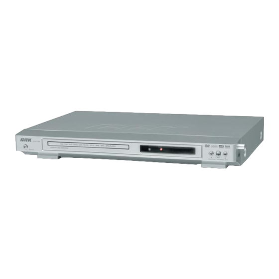
Page 4: Front Panel Illustration
Front Panel Illustration POWER POWER indicator LED POWER switch STOP button OPEN/CLOSE button MIC jack Disc tray MIC VOLUME knob IR SENSOR button PLAY/ PAUSE button... -
Page 5: Prevention Of Static Electricity Discharge
4.PREVENTION OF STATIC ELECTRICITY DISCHARGE The laser diode in the traverse unit (optical pickup)may brake down due to static electricity of clothes or human body. Use due caution to electrostatic breakdown when servicing and handling the laser diode. 4.1.Grounding for electrostatic breakdown prevention Some devices such as the DVD player use the optical pickup(laser diode)and the optical pickup will be damaged by static electricity in the working environment.Proceed servicing works under the working environment where grounding works is completed. -
Page 6: Assembling And Disassembling The Mechanism Unit
5. Assembling and disassembling the mechanism unit 5.1 Optical pickup Unit Explosed View and Part List Pic (1) - Page 7 Materials to Pic (1) PARTS CODE PARTS NAME Q ty 14692200 SF-HD60 1EA0311A06300 ASSY, CHASSIS, COMPLETE 1EA0M10A15500 ASSY, MOTOR, SLED 1EA0M10A15501 ASSY, MOTOR, SLED 1EA2451A24700 HOLDER, SHAFT 1EA2511A29100 GEAR, RACK 1EA2511A29200 GEAR, DRIVE 1EA2511A29300 GEAR, MIDDLE, A 1EA2511A29400 GEAR, MIDDLE, B 1EA2744A03000 SHAFT, SLIDE 1EA2744A03100...
-
Page 8: Bracket Explosed View And Part List
5.2 Bracket Explosed View and Part List Pic (2) Materials to Pic(2) 1.bracket 14. front silicon rubber 2.belt 15. Back silicon rubber 3.screw 16. Pick-up 4.belt wheel 17. Pick-up 5.gearwheel 18. switch 6.iron chip 19. Five-pin flat plug 7. Immobility mechanism equipment 20. - Page 9 5.3 MISCELLANEOUS 5.3.1 Protection of the LD(Laser diode) Short the parts of LD circuit pattern by soldering. 5.3.2 Cautions on assembly and adjustment Make sure that the workbenches,jigs,tips,tips of soldering irons and measuring instruments are grounded,and that personnel wear wrist straps for ground. Open the LD short lands quickly with a soldering iron after a circuit is connected.
-
Page 10: Electrical Confirmation
6.Electrical Confirmation 6.1. Video Output (Luminance Signal) Confirmation DO this confirmation after replacing a P.C.B. Measurement point Mode Disc Color bar 75% DVDT-S15 Video output terminal PLAY(Title 46):DVDT-S15 PLAY(Title 12):DVDT-S01 DVDT-S01 Measuring equipment,tools Confirmation value 200mV/dir,10 sec/dir 1000mVp-p±30mV Purpose:To maintain video signal output compatibility. 1.Connect the oscilloscope to the video output terminal and terminate at 75 ohms. -
Page 11: Video Output(Chrominance Signal) Confirmation
6.2 Video Output(Chrominance Signal) Confirmation Do the confirmation after replacing P.C.B. Measurement point Mode Disc Color bar 75% DVDT-S15 Video output terminal PLAY(Title 46):DVDT-S15 PLAY(Title 12):DVDT-S01 DVDT-S01 Measuring equipment,tools Confirmation value Screwdriver,Oscilloscope 200mV/dir,10 sec/dir 621mVp-p±30mV Purpose:To maintain video signal output compatibility. 1.Connect the oscilloscope to the video output terminal and terminate at 75 ohme. -
Page 12: Mpeg Board Check Waveform
7.MPEG BOARD CHECK WAVEFORM 7.1 27MHz WAVEFORM DIAGRAM 7.2 IC VIPER22 PIN.5 WAVEFORM DIAGRAM... - Page 13 8. Am29LV160D 16 Megabit (2 M x 8-Bit/1 M x 16-Bit) CMOS 3.0 Volt-only Boot Sector Flash Memory DISTINCTIVE CHARACTERISTICS Single power supply operation Embedded Algorithms — Full voltage range: 2.7 to 3.6 volt read and write — Embedded Erase algorithm automatically operations for battery-powered applications preprograms and erases the entire chip or any combination of designated sectors...
-
Page 14: Product Selector Guide
PRODUCT SELECTOR GUIDE Family Part Number Am29LV160D Speed Option Voltage Range: V = 2.7–3.6 V -120 Max access time, ns (t Max CE# access time, ns (t Max OE# access time, ns (t Note: See “AC Characteristics” for full specifications. BLOCK DIAGRAM –... -
Page 15: Connection Diagrams
CONNECTION DIAGRAMS BYTE# DQ15/A-1 DQ14 DQ13 DQ12 Standard TSOP RESET# DQ11 RY/BY# DQ10 BYTE# DQ15/A-1 DQ14 DQ13 DQ12 RESET# Reverse TSOP DQ11 RY/BY# DQ10... - Page 16 CONNECTION DIAGRAMS RESET# BYTE# DQ15/A-1 DQ14 DQ13 DQ10 DQ12 DQ11 FBGA Top View, Balls Facing Down BYTE# DQ15/A-1 DQ14 DQ13 RESET# DQ12 RY/BY# DQ10 DQ11 Special Handling Instructions Flash memory devices in FBGA packages may be damaged if exposed to ultrasonic cleaning methods. Special handling is required for Flash Memory products The package and/or data integrity may be compromised in FBGA packages.
-
Page 17: Pin Configuration
PIN CONFIGURATION LOGIC SYMBOL A0–A19 = 20 addresses DQ0–DQ14 = 15 data inputs/outputs A0–A19 16 or 8 DQ15/A-1 = DQ15 (data input/output, word mode), DQ0–DQ15 A-1 (LSB address input, byte mode) (A-1) BYTE# = Selects 8-bit or 16-bit mode = Chip enable = Output enable = Write enable RESET#... -
Page 18: General Description
SDRAM 16Mb H-die(x16) CMOS SDRAM 512K x 16Bit x 2 Banks SDRAM FEATURES • 3.3V power supply • LVTTL compatible with multiplexed address • two banks operation • MRS cycle with address key programs -. CAS Latency ( 2 & 3) -. -
Page 19: Pin Configuration (Top View)
SDRAM 16Mb H-die(x16) CMOS SDRAM PIN CONFIGURATION (TOP VIEW) DQ15 DQ14 DQ13 DQ12 DQ11 DQ10 LDQM N.C/RFU UDQM A10/AP 50PIN TSOP (II) (400mil x 825mil) (0.8 mm PIN PITCH) PIN FUNCTION DESCRIPTION Name Input Function System Clock Active on the positive going edge to sample all inputs. Disables or enables device operation by masking or enabling all inputs except Chip Select CLK, CKE and L(U)DQM... -
Page 20: Functional Block Diagram
SDRAM 16Mb H-die(x16) CMOS SDRAM FUNCTIONAL BLOCK DIAGRAM Data Input Register LDQM Bank Select 512K x 16 512K x 16 Column Decoder Latency & Burst Length LCKE Programming Register LRAS LCBR LCAS LWCBR LDQM Timing Register L(U)DQM * Samsung Electronics reserves the right to change products or specification without notice. Rev. -
Page 21: Key Features
8.2 MT1389 MT1389 Progressive-Scan DVD Player SOC Specifications are subject to change without notice MediaTek MT1389 is a DVD player system-on-chip (SOC) which incorporates advanced features like high quality TV encoder and state-of-art de-interlace processing. The MT1389 enables consumer electronics manufacturers to build high quality, cost-effective DVD players, portable DVD players or any other home entertainment audio/video devices. -
Page 22: General Feature List
MT1389 PRELIMINARY, SUBJECT TO CHANGE WITHOUT NOTICE MTK CONFIDENTIAL, NO DISCLOSURE General Feature List 1024-bytes on-chip RAM Super Integration DVD player single chip Up to 4M bytes FLASH-programming interface High performance analog RF amplifier Supports 5/3.3-Volt. FLASH interface Servo controller and data channel processing Supports power-down mode MPEG-1/MPEG-2/JPEG video Supports additional serial port... - Page 23 MT1389 PRELIMINARY, SUBJECT TO CHANGE WITHOUT NOTICE MTK CONFIDENTIAL, NO DISCLOSURE Audio Effect Processing TV Encoder Dolby Digital (AC-3)/EX decoding Six 108MHz/12bit DACs DTS/DTS-ES decoding Support NTSC, PAL-BDGHINM, PAL-60 MLP decoding for DVD-Audio Support 525p, 625p progressive TV format MPEG-1 layer 1/layer 2 audio decoding Automatically turn off unconnected channels MPEG-2 layer1/layer2 2-channel audio Support PC monitor (VGA)
- Page 24 9. SCHEMATIC & PCB WIRING DIAGRAM FRONT SCHEMATIC DIAGRAM...
-
Page 25: Front Schematic Diagram
FRONT SCHEMATIC DIAGRAM... -
Page 26: Power Board Schematic Diagram
POWER BOARD SCHEMATIC DIAGRAM... - Page 27 POWER BOARD SCHEMATIC DIAGRAM...
- Page 28 OK SCHEMATIC DIAGRAM...
- Page 29 OK SCHEMATIC DIAGRAM...
- Page 30 OUTPUT BOARD SCHEMATIC DIAGRAM...
- Page 31 OUTPUT BOARD SCHEMATIC DIAGRAM...
- Page 32 MIAN SCHEMATIC DIAGRAM...
- Page 33 MIAN SCHEMATIC DIAGRAM...
- Page 34 MIAN SCHEMATIC DIAGRAM...
- Page 35 MIAN SCHEMATIC DIAGRAM...
-
Page 36: Power Board
10. SPARE PARTS LIST DV911SM-2 MATERIAL LIST 1. MAIN FRONT PANEL MATERIAL CODE MATERIAL NAME SPECIFICATIONS UNIT QUANTITY LOCATION REMOTE CONTROL SOFT SPONGE SPACER 6×6×2.5 DOUBLE-FACED, HARD PCS 5232805 IR SENSOR 1PC 0000276 CARBON FILM RESISTOR 1/4W100¦ ¸ ±5% SHAPED 10... - Page 37 0680010 SCHOTTKY DIODE SR560 DO-27 U503 0880553 LM431ACZ TO-92 U503 0880581 TL431C TO-226AA(LP) U503 0880800 431L TO-92 U503 0882041 MIK431C TO-92 BC501 0210066 TERYLENE CAPACITOR 275V 104 ±20% 15mm BC501 0210070 TERYLENE CAPACITOR 275V 104 ±10% 15mm BC503 0200267 CERAMIC CAPACITOR CT81 250VAC221±20% 10mm BC503 0200268...
-
Page 38: Decode Board
0000133 CARBON FILM RESISTOR1/6W4.7K±5% SHAPED 7.5 R622,R628 0000134 CARBON FILM RESISTOR1/6W5.1K±5% SHAPED 7.5 R616 0000137 CARBON FILM RESISTOR1/6W10K±5% SHAPED 7.5 R617,R621,R620,R624,R 0000118 CARBON FILM RESISTOR1/6W10¦ ¸ ±5% SHAPED 7.5 R632,R633 0000338 CARBON FILM RESISTOR1/6W15K±5% SHAPED 7.5 R614,R618 0000341 CARBON FILM RESISTOR1/6W18K±5% SHAPED 7.5 R615 0000144 CARBON FILM RESISTOR1/6W47K±5% SHAPED 7.5... - Page 39 L210~L215,R201~R204,R 212,R228,R234,R236,R24 5,R247,R222,R251,R255, 0090001 SMD RESISTOR 1/16W 0Ω ±5% 0603 R257,R258,R298,R299,R3 03,R318,R331,R2159,R29 7,R284~R286,R287,R290, R2183,R2107,R283 R233,R261,R270,R273,R2 0090006 SMD RESISTOR 1/16W 75Ω ±5% 0603 74,R276,R280 0100034 SMD RESISTOR NETWOR 1/16W0Ω±5% 0603×4 8P RN201~RN204 0000375 CARBON FILM RESISTOR1/4W2.2Ω±5% R326 0090272 SMD RESISTOR 1/16W1Ω±5% 0603 R304~R307,R321,R340 0090003 SMD RESISTOR...
- Page 40 0310047 SMD CAPACITOR 50V 101 ±5% NPO 0603 C233,C2111,C2114,C206 0310051 SMD CAPACITOR 50V 331 ±5% NPO 0603 C212,C213 0310048 SMD CAPACITOR 50V 151 ±5% NPO 0603 C304,C306 C207,C211,C214,C216, C217,C224,C226~C231, C234~C239,C241~C254 ,C256~C259,C267~C27 4,C279,C280~C282,C30 0310084 SMD CAPACITOR 50V 104 +80%-20% 0603 1~C303,C305,C309,C31 1,C312,C2138~C2143,C 2155~C2157,C2160,C2 161,C2163,C2164,C216...
- Page 41 0780197 SMD TRIODE C1815 Q205,Q206 0780043 TRIODE 2SA1015 Q211,Q218,Q219 0780040 SMD TRIODE 3904 V305 0780193 SMD TRIODE 2SK3018 V303,V304 0780115 SMD TRIODE 2SB1132 V301,V302 0880185 NJM4558M SOP U219 0880562 4580 SOP U219 0880361 4558 SOP U219 0880322 MM74HCU04M SOP U205 0880513 HCU04 SOP U205...
Need help?
Do you have a question about the DV911SM and is the answer not in the manual?
Questions and answers