Table of Contents
Advertisement
Quick Links
Advertisement
Table of Contents

Subscribe to Our Youtube Channel
Related Manuals for BBK DV727SI


Summary of Contents for BBK DV727SI
- Page 1 DV727SI service manual...
-
Page 2: Table Of Contents
Catalog Chapter One About Maintenance 1.1 Safety precautions 1.1.1 Power supply 1.1.2 Precautions for antistatic 1.1.3 Precautions for laser head 1.1.4 About placement position 1.2 Maintenance method 1.2.1 Visualized method 1.2.2 Electric resistance method 1.2.3 Voltage method 1.2.4 Current method 1.2.5 Cutting method 1.2.6 Element substitution method 1.2.7 Comparison method... - Page 3 2.4.6 Karaoke 2.4.7 Preference 2.4.8 Parental control 2.4.9 Initial setup 2.4.10 Rest to defaults 2.4.11 Exit 2.5 Specifications Chapter Three Principle and Servicing Section One Principle of the Player 3.1.1 Function and features 3.1.2 Block diagram of the player 3.1.3 Introduction to IC used by this player Section Two Unit Circuit Principle 3.2.1 Servo circuit 3.2.2 Audio/video output circuit...
- Page 4 3.5.12 function introduction to LM431A 3.5.13 function introduction to 4558 3.5.14 function introduction to TDA1308 3.5.14 function introduction to MT1392E Chapter Four Disassembly and Assembly Process Chapter Cinque PCB board & Circuit diagram Section One PCB board Section Two circuit diagram Chapter six BOM List...
-
Page 5: Chapter One About Maintenance
Chapter One About Maintenance 1.1 Safety precautions 1.1.1 Power supply When maintenance personnel are repairing DVD players, he should pay special attention to power board with 220V AC and 330V DC which will cause hurt and damage to persons! 1.1.2 Precautions for antistatic Movement and friction will both bring static electricity which causes serious damages to integrated IC. -
Page 6: About Placement Position
1.1.4 About placement position 1. Never place DVD player in positions with high temperature and humidity. 2. Avoid placing near high magnetic fields, such as loudspeaker or magnet. 3. Positions for placement should be stable and secure. 1.2 Maintenance method 1.2.1 Visualized method Directly view whether abnormalities of collision, lack of element, joint welding, shedding welding, rosin joint, copper foil turning up, lead wire disconnection and elements burning up among pins of... -
Page 7: Element Substitution Method
1.2.6 Element substitution method When some elements cannot be judged good or bad, substitution method may de adopted directly. 1.2.7 Comparison method A same good PC board is usually used to test the correct voltage and waveform. Compared these data with those tested through fault PC board, the cause of troubles may be found. Through the above maintenance method, theoretical knowledge and maintenance experience, all difficulties and troubles will be readily solved. -
Page 8: Chapter Two Functions And Operation Instructions
Chapter Two Functions and Operation Instructions 2.1 Features This player has employed the new generation DV decode chip with built-in Dolby Digital decoder which will bring you to a brand-new AV entertainment world. The 2-laser super error-correction mechanism supports CD-R. Brand-new AV Effects #Compatible with DivX, MPEG4 discs to produce wonderful pictures. -
Page 9: Control Button Locations And Explanations
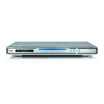
2.2 Control Button Locations and Explanations 2.2.1 Front Panel Illustration 9 10 Headphone Jack Power indicator Push button MIC Jack Disc tray PREV button POWER switch OPEN/CLOSE button PAUSE button IR SENSOR PLAY button NEXT button Display window STOP button Slot flap for USB 2.2.2 Rear Panel Illustration HDMI Out jack... -
Page 10: Remote Control Illustration
2.2.4 Remote Control Illustration Button Open or close the disc tray. LANG Button Change the audio language or audio channel. MEMORY Button Save the playing point or jump to the saved point . DISP Button Display or hide disc information. NUMBER Buttons BROWSE Buttons switch new user interface. -
Page 11: Accessories
5.Press [LEFT] button if you want to return to the 2.3 Accessories previous setup page. AUDIO/VIDEO CORD 1PCS 6.Press [SETUP ]to exit the setup menu. REMOTE 1PCS 2.4.2 Language AAA SITE BUTTERIES 2PCS WARRANTY CARD 1PCS Setup menu Russian USER MANUAL 1PCS DVD menu English... -
Page 12: Sound
#Optional setting: S-Video,Component , SCART. #Optional setting: Stereo, 5.1. #Default: Component. #Default: Stereo. #When using RGB outputs from the SCART B.Stereo mix: To set the output means of the interface,please select RGB. Other wise , left or right audio when playing a Dolby disc please select Com-ponent,and when using S- with separate two-channel audio. -
Page 13: Playback
d. Press [OK] or [LEFT] to return to the Delays in 1. DVD:set whether information of advertisement channels setting page. and warnings at the beginning of DVD disc is G. PRO Logic II: To set PRO Logic II to ON or skipped to play the movie directly. -
Page 14: Preference
4.Echo: 2. Set password: To set four digit password to A.In microphone setup page, press [UP/DOWN] enable you to change the parental control cursor to select “Echo” item, and then press ratings. [OK] button to enter the adjustment menu. #Default: 7890. B.Press [UP/DOWN] cursor to adjust the setup value. - Page 15 MIC input,USB Inputs Analog audio output: Stereo, output 5.1CH Audio outputs Digital audio output: Coaxial,Opcical Composite, S-Video, component Y Cb Cr, progressive scan Outputs Video outputs output Y Pb Pr, RGB/SCART Headphones output Video amplitude 1.0Vp-p(75 ) S-Video amplitude Y:1.0Vp-p(75 ) C:0.286Vp-p(75 ) Video Characteristics Component Video amplitude Y:1.0Vp-p(75 )
-
Page 16: Chapter Three Principle And Servicing
Chapter Three Principle and Servicing Section One Principle of the Player 3.1.1 Functionandfeatures This model adopts new generation DVD decode chip, with built-in Dolby decoder and realistic surround system, which brings you vivid and real movie effect. It has the following features: Progressive scanning output to produce steadier and clearer pictures without flickering. - Page 17 SDRAM 64M FLASH16M Panel CS4340 MIC board U208 U207 Audio amplifying filtering U209 U210 output U211 terminal ASPDIF CVBS Video CVBS filtering CB/B clamping CR/R Power DV33 HDMI SCL# board U216 AVCC HDMI SDA# Mt1389 B VSYNC# HSYNC# U201 INT0# VR-DVD ROUT# DVI jack...
-
Page 18: Introduction To Ic Used By This Player
3.1.3 Introduction to IC used in this player Introduction to IC used in DV727SI is shown in the following table: PCB semi-finished IC model Location Function product name MT1389B U201 Decode chip 24C02 U202 EEPROM MT1392C U203 HDMI control HCU04... -
Page 19: Section Two Unit Circuit Principle
Section Two Unit Circuit Principle 3.2.1 Servo circuit 1. DV727SI adopts SANYO 62 decoder and MTK decode solution (MT1389+FLASH(16M)+SDRAM (64M)). The servo circuit is mainly composed of front signal processing, digital servo processing, signal processing IC T1389 and drive circuit D5954, in which MT1389 is the main component of decode circuit at the same time. - Page 20 2. Working principle: after powering on or disc in, according to IOA signal, disc identification circuit decides through which path of variable resistor the laser detecting diode gets path to the ground, meanwhile MT1389 decides whether DVD laser or VCD laser is emitted according to IOA signal, which can be fulfilled through laser power control circuit.
-
Page 21: Audio/Video Output Circuit
TROPEN is set high level by MT1389, open/clode electric machine tuns conversely to bring along disc tray to close. After disc tray closing to proper position, signal of closing to proper position (TR_IN) is set low level through the detecting switch on loader frame, MT1389 pulls down TROPEN and electric machine stops running to finish “close”... -
Page 22: Mute Circuit And Power-Off Quieting Circuit
Damage with advantages that there is no extra loss during the course of transmission; digital signals and analog signals may be transmitted at the same time; transmission speed may be increased; resolution is not controlled by SXGA; usage is simple and cost is reduced. Shown in the figure 3.2.2.1, it HDMI structure, “Source”... -
Page 23: Reset Circuit
Analog channel to make the switching tube and make audio signal bypass into ground to reach the Purpose of mute. The working mechanism is that when no audio signal comes to a certain path, CS4360 changes the mute control signal corresponding with this path to high level. After pressing MUTE button, 3-path mute signals all change to high level. -
Page 24: Power Supply Circuit
2. Working principle: after power on, Dv33 voltage increases to 3.3V quickly, main chip power supply is normal, because the voltage to ground of C271, C272 cannot change suddenly, the input end of U205C shows low electric potential, now reset signal URST keeps low level to perform reset to main chip. - Page 25 2. Working principle: this power circuit is responsible for the module circuit power supply of this player. Working principle of each part is shown as follows: (1) Electromagnetic disturbance filter circuit: for various electromagnetic radiation exist outside, the input AC will be affected. The function of electromagnetic disturbance filter capacitor is to filter these disturbance to make those that enter bridge rectification circuit are pure 220V AC.
- Page 26 (4) A-9V , A+9V: used to supply power for audio power amplifying chip F4558 and mute circuit. (5) D+3V3: power supply of MT1389, FLASH, U211SDRAM and 74HCU04. (7) A+5V (pin 1, 2 of XS504): supply power for power amplifier board A/D conversion ship Cs5340. - 22 -...
-
Page 27: Section Three Servicing Cases
Section Three Servicing Cases 3.3.1 Servicing cases [ Example 1 ] Symptom: power not on Description: connect with power, standby indicator light is not on and player cannot power on. Analysis and troubleshooting: test power board5V, 3.3V voltage and it is normal; check power supply of decode board 1389 chip and it is 3.3V, 1.8V, which is normal;... - Page 28 [ Example Symptom: no MIC Description: when reading disc, sound is normal, there is picture but no microphone function. Analysis and troubleshooting: power on, use remote controller to switch on MIC, insert microphone, use oscillograph probe to test OKA pin of MIC board Xs601, speak toward it and there is signal output; check decode board U210 OKR, OKL and there is signal input;...
- Page 29 [ Example 9 ]Symptom: HDMI has no sound output Description: HDMI has picture but no sound, AV is normal. Analysis and troubleshooting: check U203 Mt1392 power supply voltage 1.8V, DV3.3V and they are normal; check pin 25 of U203 rest voltage and it is 3.3V, which is normal; check 3 audio data outputted by 1389, use oscillograph to test pin 75 of U203 and find that SDATA1 has no audio data input;...
- Page 30 Analysis and troubleshooting: this trouble often appears in video decode part; after power off for a period, picture output is normal; after playing for a period (about 5 minutes), picture has interference; to analyse this trouble, play DVD disc normally firstly, use iron to heat chip 1389; after heating, picture has interference;...
-
Page 31: Troubleshooting Flow Chart
3.3.2 Troubleshooting flow chart 1. Troubleshooting process for “Power not on” is shown in the figure 3.3.2.1: Whether 3.3V, 5V on power Check 3.3V, 5V voltage Power not on board are stabilizing circuit normal Whether 1389 core voltage Check decode board 1.8V, 1.8V, 3.3V are 3.3V power supply circuit normal... - Page 32 2. Troubleshooting process for “No MIC” is shown in the figure 3.3.2.2: Change ZD502 voltage No MIC stabilizing tube Whether Whether Whether -21V power supply ZD501 voltage stabilizing power board 9V voltage Whether Q501 is normal is normal tube is normal is normal Change D511 Change Q501...
- Page 33 3. Troubleshooting process for “No sound” is shown in the figure 3.3.2.3: No sound Whether power board Check each voltage 5V, 3.3V power supply stabilizing circuit is normal Whether each operational amplifier IC4558 power Change X203 flat cable supply of decode board is normal Whether...
- Page 34 4. Troubleshooting process for “Power not on” is shown in the figure 3.3.2.4: Power not on Whether Whether power supply D501, D513, Change relevant elements 3.3V, 5V voltage L507, L508 are is normal normal Whether Whether reset circuit is Change transformer transformer is normal Check reset circuit normal...
-
Page 35: Section Four Waveform Diagram
Section Four Waveform diagram This section collects signal waveform diagram of audio, video and each unit circuit with the purpose to help servicing personnel to judge where trouble lies in accurately and quickly to improve servicing skills. For the difference of oscillograph's type, model and tuner, a certain difference may exist, so the servicing personnel are expected to pay more attention to check in daily operation. - Page 36 3. A signal waveform diagram of pin 9 of XS301(B C D E F 4. DMO signal (when there is main axis rotation) waveform diagram of pin 37 of U201 (Mt1389) 5. FMO signal (when there is feed) waveform diagram of pin 38 of U201 (MT1389) - 32 -...
- Page 37 6. TRO signal (when there is trace) waveform diagram of pin 41 of U201 (MT1389) 7. FOO signal (when there is focus) waveform diagram of pin 42 of U201 (MT1389) 8. Waveform diagram of pin 29 (when no disc in) of U214(FLASH) - 33 -...
- Page 38 9. Waveform diagram of pin 38of U211 (SDRAM) 10. Video signal waveform diagram 11. ACLK (12.2878MHZ): waveform diagram for external clock signal - 34 -...
- Page 39 12. ABCK (3.07195MHZ): waveform diagram for bit clock signal 13. ALRCK (48KHZ): waveform diagram for left/right channel clock signal 14. SDATA0: waveform diagram for mixed left/right channel digital signal - 35 -...
- Page 40 15. SDATA1: waveform diagram for surround left/right channel digital signal (now the disc being played is 2.1CH, and this signal has no output; if 5.1CH, the form is the same with that of SDATA0) 16. SDATA2: waveform diagram for centre subwoofer digital signal 17.
- Page 41 18. LEF#: waveform diagram for subwoofer channel analog signal 19. AMDAT: waveform diagram for microphone signal after 5340 A/D conversion 20. SPDIF: waveform diagram for optical/coaxial digital audio signal - 37 -...
- Page 42 21. 27M clock signal waveform diagram 22. Reset circuit waveform diagram URST# Dv33 - 38 -...
-
Page 43: Section Five Function Introduction To Ic
Section Five Function Introduction to IC 3.5.1 Function introduction to MT1389HD 1. Description MT1389HD (U201) is a cost-effective DVD system-on-chip (SOC) which incorporates advanced features like MPEG-4 video decoder, high quality TV encoder and state-of-art de-interlace processing. Based on MediaTek’ s world-leading DVD player SOC architecture, the MT1389E is the 3rd generation of the DVD player SOC. - Page 44 (2)High Performance A nalog RF Amplifier Programmable fc Dual automatic laser power control Defect and blank detection RF level signal generator (3)Speed Performance on Servo/Channel Decoding DVD-ROM up to 4XS CD-ROM up to 24XS (4)Channel Data Processor Digital data slicer for small jitter capability Built-in high performance data PLL for channel data demodulation EFM/EFM+ data demodulation Enhanced channel data frame sync protection &...
- Page 45 Provides the self-refresh mode SDRAM Block-based sector addressing (9)Video Decode Decodes MPEG1 video and MPEG2 main level, m ain profile video (720/480 and 720x576)Decodes MPEG-4 Advanced Simple Profile Support DivX 3.11/4.x/5.x Home Theater Profile Support Nero-Digital Smooth digest view function with I, P and B picture decoding Baseline, extended-sequential and progressive JPEG image decoding Support CD-G titles (10)Video/OSD/SPU/HLI Processor...
- Page 46 (12)TV Encoder Four 108MHz/12bit DACs Support NTSC, PAL-BDGHINM, PAL-60 Support 525p, 625p progressive TV format Automatically turn off unconnected channels Support PC monitor (VGA) Support Macrovision 7.1 L1, Macrovision 525P and 625P CGMS-A/WSS Closed Caption (13)Progressive Scan Video Automatic detect film or video source 3:2 pull down source detection Advanced Motion adaptive de-interlace Minimum external memory requirement...
- Page 47 DVDRFIN Analog input AC coupled DVD RF signal input RFIN Analog input DC coupled main beam RF signal input A Analog input DC coupled main beam RF signal input B Analog input DC coupled main beam RF signal input C Analog input DC coupled main beam RF signal input D Analog input...
- Page 48 Negative main beam summing output SGND Ground Analog ground Analog output Focus error monitor output Analog output Tracking error monitor output TEZISLV Analog output TE slicing Level Analog monitor output (6) RFVDD3 Analog output Analog Power RFRPDC Analog Input RF ripple detect output RFRPAC Analog output RF ripple detect input(through AC-coupling)
- Page 49 Focus servo output. PDM output of focus servo Analog output compensator LVTTL3.3 Input, Monitor hall sensor input ADIN1 Schmitt input, pull up, AD input 1 (Digital pin) GPIO with analog input path GPIO for ADIN1 General Power/Ground (18) DVDD18 Power 1.8V power pin for internal digital circuitry DVSS Ground...
- Page 50 InOut 4~16mA,SRPU Microcontroller address/data 6 InOut 4~16mA,SRPU Microcontroller address/data 5 InOut 4~16mA,SRPU Microcontroller address/data 4 InOut 4~16mA,SRPU Microcontroller address/data 3 InOut 4~16mA,SRPU Microcontroller address/data 2 InOut 4~16mA,SRPU Microcontroller address/data 1 InOut 4~16mA,SRPU Microcontroller address/data 0 IOA 0 InOut 4~16mA,SRPU Microcontroller address IOA 1 InOut 4~16mA,SRPU Microcontroller address 1/ IO...
- Page 51 InOut 4~16mA, UWR# Microcontroller write strobe, active low SRPD,SMT InOut 4mA, URD# Microcontroller read strobe, active low SRPD,SMT InOut 4~16mA, UP1_2 Microcontroller port 1-2 SRPD,SMT InOut 4mA, UP1_3 Microcontroller port 1-3 SRPD,SMT InOut 4mA, UP1_4 Microcontroller port 1-4 SRPD,SMT InOut 4mA, UP1_5 Microcontroller port 1-5 SRPD,SMT...
- Page 52 I) Serial interface port 0 data-in II) GPIO 1) Audio left/right channel clock of SPDIF input SPLRCK SDO0 Inout 2) While SPDIF input is not used: I) Serial interface port 0 data-out II) GPIO 1) Audio bit clock of SPDIF input SDCS0 2) While SPDIF input is not used: SPBCK...
- Page 53 4) While using external channels: I) GPO_1 1) Audio serial data 2 (Center/LFE) 2) DSD data right surround channel 3) Trap value in power-on reset: InOut 4mA, ASDATA3 I) 1: manufactory test mode PD,SMT II) 0: normal operation 4) While only 2 channels output: I) GPO_0 1) Audio serial data 3 (Center-back/ Center-left-back/Center-right-back, in 6.1 or 7.1 mode)
- Page 54 b. GPIO AVCM Analog AUDIO DAC reference voltage 1) AUDIO DAC Left Surround channel output 2) While internal AUDIO DAC not used: GPIO Output a. SDATA2 b. GPIO 1) AUDIO DAC Left Surround channel output 2) While internal AUDIO DAC not used: GPIO Output a.SDATA0...
- Page 55 Output 1) Video data output bit 6 YUV 6 R/Cr/Pr 4MA, SR 2) Red or CR 1) Vertical sync input/output 2) While no External TV-encoder: Output VSYN V_ADIN1 I) Vertical sync for video-input 4MA, SR II) Version AD input port 1 III) GPIO 1) Video data output bit 7 2) While no External TV-encoder:...
- Page 56 MISC (12) InOut PRST# Power on reset input, active low PD,SMT InOut PD,SMT Microcontroller ICE mode enable XTALO Output 27MHz crystal output XTALI Input 27MHz crystal input USB_VSS USB Ground USB ground pin USBP Analog Inout USB port DPLUS analog pin USBM Analog Inout USB port DMINUS analog pin...
- Page 57 IO_9(RD2 1) Digital Video output Y bit 0 InOut Non-pull 2) GPIO IO_10(RD 1) Digital Video output Y bit 1 InOut Non-pull 2) GPIO IO_11(RD 1) Digital Video output Y bit 2 InOut Non-pull 2) GPIO IO_12(RD 1) Digital Video output Y bit 3 InOut Non-pull 2) GPIO IO_13(RD...
- Page 58 RWE# output DRAM Write enable, active low DQM1 InOut Data mask 1 IO_18 (DQS1) InOut Non-pull GIPIO InOut DRAM data 8 InOut DRAM data 9 RD10 InOut DRAM data 10 RD11 InOut DRAM data 11 RD12 InOut DRAM data 12 RD13 InOut DRAM data 13...
-
Page 59: Function Introduction To At24C02
3.5.2 function introduction to AT24C02 1. Description The AT24C02 (U202) provides 2048 bits of serial electrically erasable and programmable read-only memory (EEPROM) organized as 256 words of 8 bits each. The device is optimized for use in many industrial and commercial applications where low-power and low-voltage operation are essential. The AT24C02 is available in space-saving 8-lead PDIP, 8-lead MAP, 8 lead TSSOP and 8-ball dBGA2 packages and is accessed via a 2-wire serial interface. -
Page 60: Function Introduction To Cs5340
Serial SCL input TEST Test port Positive Power Supply 3.5.3 function introduction to C S 5 3 4 0 1. DESCRIPTION The CS5340 (U203) is complete analog-to-digital converter for digital audio systems. It performs sampling, analog-to-digital conversion and anti-alias iltering, generating 24-bit values for both left and right inputs in serial form at sample rates up to 200 kHz per channel. -
Page 61: Function Introduction To 74Hcu04
SCLK Serial clock FILT+ Positive voltage reference LRCK Left right clock Mode selection 1 3.5.4 function introduction to 74HCU04 1. Description The 74HCU04 (U205) is a high-speed Si-gate CMOS device and is pin compatible with low power Schottky TTL (LSTTL). It is specified in compliance with JEDEC standard no. 7A. The 74HCU04 is a general purpose hex inverter. -
Page 62: Function Introduction To Sdram
Chip enable, low level effective 27、46 Ground Output enable signal , low level is effective 29-3、6、38-44 DQ0-DQ14 15 bit data bus 5V power supply Take word extend mode as data line, and bit extend DQ15/A-1 mode as address line Select 8-bit or 16-bit output mode. -
Page 63: Function Introduction To 4580
3.3V power supply Ground Data input/output screen-shielded LDQM Data bus signal Write control signal VDDQ 3.3V power supply Line address gating signal Data bus Row address gating signal DQ10 Data bus Chip selection signal VSSQ Ground SD-BS0 Segmanr address 0 gating signal DQ11... -
Page 64: Function Introduction To D5954
3. PIN Description Description PIN No Symbol Output 1 1OUT Inverting Input Pin 1 1IN– Non-Inverting Input Pin 1 1IN+ Negative Power Supply VCC– Non-Inverting Input Pin 2 2IN+ Inverting Input Pin 2 2IN– Output 2 2OUT Positive Power Supply VCC+ 3.5.8 function introduction to D5954 1. -
Page 65: Function Introduction To Pt6961
VOTK+ Trace drive forward direction voltage output VOTK- Trace drive reverse voltage output VOLD+ Feed drive forward direction voltage output VOLD- Feed drive reverse voltage output PGND Ground VINFTK Trace feedback signal input PVCC2 5V power supply PREGND Ground VINLD Feed control signal input CTK2 External feedback loop... - Page 66 DOUT Data output Data input Clock input Serial interface strobe Key data input Key data input Key data input Power supply SG1/KS1 Segment output SG2/KS2 Segment output SG3/KS3 Segment output SG4/KS4 Segment output SG5/KS5 Segment output SG6/KS6 Segment output SG7/KS7 Segment output SG8/KS8 Segment output...
-
Page 67: Function Introduction To Viper22Adip
3.5.10 function introduction to VIPer22ADIP 1. DESCRIPTION The VIPer22A (U501) combines a dedicated current mode PWM controller with a high voltage Power MOSFET on the same silicon chip. Typical applications cover off line power supplies for battery charger adapters, standby power supplies for TV or monitors, auxiliary supplies for motor control, etc. The internal control circuit offers the following benefits: Large input voltage range on the VDD pin accommodates changes in auxiliary supply voltage. -
Page 68: Function Introduction To Lm431A
outputs from position D. The higher of the voltage inputted from the right side, the stronger of the light emitted from light emitting diode and the larger of the photocurrent produced from position D. The lower of the voltage inputted from the right side of photoelectric coupler, the weaker of the light emitted from light emitting diode and the weaker of the current outputted from position D. -
Page 69: Function Introduction To Tda1308
operation over the full military temperature range of – 55 C to 125 C. 2. FEATURES ◆ Continuous-Short-Circuit Protection ◆ Wide Common-Mode and Differential ◆ Voltage Ranges ◆ No Frequency Compensation Required ◆ Low Power Consumption ◆ No Latch-Up ◆ Unity-Gain Bandwidth ,3 MHz Typ ◆... -
Page 70: Function Introduction To Mt1392E
2. FEATURES ◆ Wide temperature range ? ◆ No switch ON/OFF clicks ? ◆ Excellent power supply ripple rejection ? ◆ Low power consumption ◆ Short-circuit resistant ? ◆ High performance ◆ – high signal-to-noise ratio ◆ – high slew rate ◆... - Page 71 Support 480i, 576i, 480p, 576p digital video input According to CCIR656 or CCIR601 spec. Support 720p (50/59.94Hz), 1080i? ? (50/59.94Hz) digital video input According to SMPTE-293M spec. Programmable scaler converts standard-definition video to 720p, 1080i high-definition video. TV encoder support 480p, 576p, 720p, 1080i (50 and 59.94Hz) component analog output including RGB and YCbCr.
- Page 72 DVDD18 Power of digital core, 1.8V PWDN# I, PD Power down, activ e low RST# I, PD Reset, active low. XTAL Normal : clock input VDAC test : VDAC test clock input Interrupt output DVSS Digital ground IO,PD Power ON : Serial interface address 7 A7/GPO0 IO,PD BIST mode : SRAM fail output...
- Page 73 VDAC test : PLL test Enable BIST mode SRAM fail output GPIO10 Normal : General purpose output H-sync in out / HDMI test input VDAC test : PLL test calibration HTPLG I,PD HDMI Hot- Plug detection AVSS Analog ground PLLC0 PLL Capacitor ground PLLC1 PLL Capacitor...
- Page 74 Normal : S/PDIF audio input SPDIF SCAN mode : test _se input VDAC test : VDAC test reset, active low BIST mode : BIST reset, active low. Normal : I 2 S data of channel 6/7 VDAC test VDAC test data bit 11 input Normal : I 2 S data of channel 4/5 VDAC test : VDAC test data bit 10 input BIST mode : BIST reset active low...
-
Page 75: Chapter Four Disassembly And Assembly Process
Chapter Four Disassembly and Assembly Process DVD players manufactured in BBK are largely identical but with minor differences and are mainly composed of loader components, control panel components, decode and servo board components, power board components, power amplifier board components, MIC board components and AV board components. -
Page 76: Chapter Cinque Pcb Board & Circuit Diagram
Chapter Cinque PCB board & Circuit diagram Section One PCB board 5.1.1 Surface layer of KEY SCAN Board TC402 LED402 U402 LED401 K401 XS402 LED403 XS401 TC401 4997-3 DVD 2005/08/05 - 72 -... - Page 77 5.1.2 Bottom layer of KEY SCAN Board DZ403 R405 R403 C405 DZ407 DZ401 C403 C404 R414 C411 R413 Q401 R411 DZ402 R402 R410 DZ406 C410 C402 R409 R412 C409 R408 C401 U401 DZ408 Q402 DZ405 R419 R404 R418 L401 DZ409 C406 DZ404 - 73 -...
- Page 78 5.1.3 Surface layer of DECODE&SERVO Board 1 . 1 + - 0 . 0 5 m m 1 . 0 5 1 . 1 5 R740 C752 C733 R741 JK706 JK705 JK702 R730 C734 D201 D202 D203 D204 D205 D206 D207 C735 JK701...
- Page 79 5.1.4 Bottom layer of DECODE&SERVO Board C308 R295 R294 R215 RN202 L235 C244 C234 C318 C258 R2165 C242 C247 C241 C245 R333 C207 R332 C214 C2167 C246 L201 C282 C254 C2170 C294 C2166 C215 C2171 C2169 C2168 C2163 D223 C281 C280 C309 V310...
- Page 80 5.1.5 Surface layer of MIC Board XS601 G602 JP606 TC615 U601 JP602 JP607 G601 TC605 TC616 TC601 JP605 R629 R611 XS603 TC617 JP601 TC619 TC614 TC618 TC620 JP608 G603 6977K-0 AGND MIC601 JK601 DVD 2004/9/13 - 76 -...
- Page 81 5.1.6 Bottom layer of MIC Board R621 C601 R607 R606 C609 R602 R604 L601 C602 R603 C605 R623 Q601 R601 R627 C616 R633 L604 R631 R628 U603 C604 R632 R626 R636 C617 R634 - 77 -...
-
Page 82: Power Board
5.1.7 Power Board CN503 L505 D508 TC501 C508 HIGH R503 R513 VOLTAGE T501 G503 TC503 G501 D507 BC505 R514 CN501 TC504 JP505 L509 AGND D505 BCN501 JP504 TC506 TC515 ~220V C518 JP501 L507 R516 AGND C503 D503 TC508 BCN503 D510 D504 ~220V ZD502... - Page 83 Grid1 Grid1 DZ405 DZ406 DZ407 Grid2 CLOCK DATA Grid2 R401 1N4148-SE 1N4148-SE 1N4148-SE LED402 Grid3 Grid3 C401 Grid4 Grid4 121(DNS) R420 Grid5 Grid5 R402 R411 5.1K 100R CLOCK Grid6 Grid6 LED2 C402 Grid7 R412 Grid7 121(DNS) 5.1K Q401 Seg1 Seg1/ks1 R403 3904 Q402...
- Page 84 U211 DMA0 DMA1 DMA2 UPD[15..0] DMA3 U214 DMA4 UPA[20..0] L243 1.8uH DMA5 1*16MBit_FLASH(TSOP) DMA6 VIDEO_C D209 DMA7 1N4148*2 DMA8 BYTE R261 C289 C290 DMA9 47pF 47pF DMA10 DQ10 A10/AP DQ10 DQ15/A-1 DMA11 DQ11 DQ11 DQ12 AD14 VGND BA0/A13 DQ12 DQ14 DBA1 DQ13 VGND...
- Page 85 AVCC V1P4 C222 TC202 R215 R308 R309 R205 20pF 10uF/16V JITFO C233 JITFN L205 C223 L206 C240 C218 100K FBSMT 0R(DNS) RFVDD3 DV33 AVDD3 FBSMT R223 DV33 R311 VREFN VREFP R227 DACVDD3 750K/1% 2N3904 C231 C232 L203 V305 DVD: 0V C238 C239 CD: +3.3V...
- Page 86 AVCC DV33 TC236 C2155 10uF/16V(DNS) C2138 C2139 C2140 C2153 TC231 R2132 C2154 U207 R2129 24K 20K(DNS) 10uF/16V(DNS) MUTE1 MUTEC1 AGND SDATA0 SDIN1 AOUTA1 C2111 SDATA1 SDIN2 AOUTB1 SDATA2 MUTE2 R2136 SDIN3 MUTEC2 R2130 R2131 SBCLK 4.7K 4.7K 6.8K SCLK AOUTA2 XS204 TC240 SLRCK...
- Page 87 C616 JK601 PHONEJACK TC617 TC619 47uF/16V R631 100uF/16V R625 R622 3.9K R633 -9VA 4.3K C619 R627 104(NC) R605 TC616 C602 47uF/16V 10k(NC) R635 C621 R637 104(NC) R629 22R(NC) AGND 3.3K XS603 Q601 R621 8050D +9VA C604 R630 TC614 3.3K AGND R638 47uF/16V R601...
- Page 88 L701 FBSMT L709 C701 VIDEO_Y1 GREEN FBSMT C707 20pF L702 LFE## C720 R705 FBSMT R701 75R(DNS) C702 IEC958 BLACK 220R R702 C710 100R 20pF R714 L703 V701 SL## FBSMT 8050(DNS) L707 2.2K(DNS) C703 VIDEO_U AGND BLUE RGB_CVBS FBSMT C708 C718 R713 20pF L704...
- Page 89 DV33 DV33 DV33 DV33 1392_DACVDD3 U204 C748 C749 C750 AT24C04(DNS) FS_1392 C730 R716 R727 C744 C745 TX2HO+ TX2HO- VREF_1392 D215 D216 DC/NC HGND RST_/NC RST/WP 1N4148*2 1N4148*2 MSCK DV33 DV33 WP/RST_ C746 R724 560R C731 C732 HGND HGND 101(DNS) 101(DNS) TX2O+ TX2O- R723...
- Page 90 L505 D508 HER105 10uH/1A TC503 TC504 C508 220uF/25V 220uF/25V D507 L509 HER105 10uH/1A LED+5V SA+5V TC515 R514 R503 C502 1000uF/10V D502 D503 470R JP501 39K/2W 103/1KV 1N4007 1N4007 L507 HER303 D510 10uH/2A TC505 TC506 TC501 C511 D501 1000uF/10V 1000uF/10V D504 22uF/400V D505 1N4007...
-
Page 91: Chapter Six Bom List
Chapter six BOM List MATERIAL MATERIAL NAME SPECIFICATIONS LOCATION CODE DV727SI(RU)SILVER[1389B] DECODE BOARD: 2988-2 1.1/Ver7.1 R222,R245,R247,R248,R251,R257,R258,R297 0090001 SMD RESISTOR 0000001 ~R299,R318,R342,R718,R726,R2159,R269,R2 32,R275,R272,R728,R729 0090272 SMD RESISTOR 1/16W 1O±5% 0603 R304~R307,R321 0090002 SMD RESISTOR 1/16W 2.2O ±5% 0603 R706 0090003 SMD RESISTOR 1/16W 10O±5% 0603... - Page 92 MATERIAL MATERIAL NAME SPECIFICATIONS LOCATION CODE PRECISION SMD 0090609 1/16W 100O±1% 0603 R243,R265 RESISTOR PRECISION SMD 0090626 1/16W 200O±1% 0603 R242 RESISTOR PRECISION SMD 0090319 1/16W 750K±1% 0603 R227 RESISTOR CARBON FILM 00003759 1/4W2.2O±5% BELT R326 RESISTOR TC201,TC202,TC221~TC230,TC232,TC233,TC2 02604379 CD CD11 16V10U±20%5×11C5 BELT 40,TC241 TC203,TC210,TC237,TC247,TC302,TC303,TC3...
- Page 93 MATERIAL MATERIAL NAME SPECIFICATIONS LOCATION CODE C207,C209,C211,C214,C216,C217,C224,C226 ~C228,C230~C232,C234~C239,C241~C254,C2 56~C259,C267,C274,C279~C281,C301~C303, C305,C311,C312,C323,C325~C329,C714,C715 0310543 SMD CAPACITOR 50V 104±10% X7R 0603 ,C720,C730,C736~C740,C742~C746,C748~C7 51,C2106,C2138~C2143,C2150~C2157,C2163, C2166~C2171,C2174,C2175,C287,C284,C270, C308,C283,C208,C331,C721 ⑿ 0310362 SMD CAPACITOR 16V474 +80%-20% Y5V 0603 C218 C201~C204,C221,C240,C272,C291,C317~C32 0310234 SMD CAPACITOR 16V 105 +80%-20% Y5V 0603 2,C268,C285,C286,C271,C297 0390355 SMD INDUCTOR 4.7UH±10% 1608 L305,L308...
- Page 94 SA-001-012 BLACK IRON PIECE,SCREEN- 1910129 TERMINAL SOCKET JK703 SHIELDED 1860029 SCART SOCKET SCART-01 JK706 1860102 HDMI 51U019S-333N-A JK708 1633140 2988-2 DV727SI(RU)SILVER[1389B] MAIN PANEL 5446036 LIGHT TOUCH RESTORE 1340003 HORIZONTAL 6×6×1 K401 SWITCH 0620002 RADIATION DIODE F3 RED LED401 0260254 CD11C 10V100U±20%6×5 2.5 TC401,TC402 ⑦...
- Page 95 SMD DOUBLE DIODE MMBD4148SE SOT-23 DZ401~DZ409 0390095 SMD MAGNETIC BEADS FCM1608K-221T05 L401 0780040 SMD TRIODE 3904(100-300) SOT-23 Q401 1632607 4997-3 DV727SI(RU)SILVER[1389B] OK BOARD 5446732 0090003 SMD RESISTOR 1/16W 10O±5% 0603 R621,R622 0090009 SMD RESISTOR 1/16W 330O±5% 0603 R601 0090012 SMD RESISTOR 1/16W 560O±5% 0603...
- Page 96 1563391 6977K-0 3P450 2.0 T2 1P SHIELD,WITH 2150258 FLAT CABLE XS603 NEEDLE,TOGETHER DIRECTION 28#线 2100010 LEAD F0.6 SHAPED 5mm JP601 ~ JP608 1980046 EARPHONE SOCKET ST-301-030-100 JK601 GROUND CHIP OF 3870115 AB903 G601, G602 POWER BOARD DV727SI(RU)SILVER[1389B] - 92 -...
- Page 97 MATERIAL MATERIAL NAME SPECIFICATIONS LOCATION CODE POWER BOARD 5446731 2100010 LEAD F0.6 SHAPED 5mm JP502,JP510,JP519,JP520 2100003 LEAD F0.6 SHAPED 7.5mm JP501,JP509,JP514,JP516,JP518 2100004 LEAD F0.6 SHAPED 10mm JP511 CARBON FILM 0000273 1/4W33O±5% SHAPED 10 R505 RESISTOR CARBON FILM 0000362 1/4W220O±5% SHAPED 10 R515 RESISTOR CARBON FILM...
- Page 98 F501 ⒇ 2300028 FUSE T1.6AL 250V WITH LEAD FEET F502 ⒇ GROUND CHIP OF 3870115 AB903 G503 POWER BOARD 1563850 @5977K-5 UL DV727SI(RU)SILVER[1389B] REMOTE CONTROL 5471742 0310048 SMD CAPACITOR 50V 151±5% NPO 0603 C802,C803 0630009 EMISSION PIPE TSAL4400 LED801 D801~D803 (21) 0700007...
- Page 99 RC026 ANODE/CATHODE 3850126 RC026 SPRING CONDUCT GLUE OF 4631052 RC026-01R 4# REMOTE CONTROL 5070070 GLUE BAG 85×250 DV727SI(RU)SILVER[1389B] SUBSIDIARY PANEL 5446037 0620076 RADIATION DIODE 3B3HC COLORLESS WITH BLUE LED903 0620040 RADIATION DIODE 3B 4SC WHITE ISSUE BLUE LED901,LED902 1940008 SOCKET 8P2.0mm...
- Page 100 TC901 (24) 0260201 CD11C 16V100U±20%6×7 2.5 1940022 SOCKET 4P 2.0mm XS901 1860047 USB SOCKET CAM-B85-4Pin JK901 1633044 A725SI-1 DV727SI(RU)SILVER[1389B] PROGRAM FLASH ROMDV727SIRU-0A(16M) 0911717 U214 (25) 0881650 29LV160BE-70PFTN TSOP U214 (25) 0881651 M29W160EB 70N6 TSOP - 96 -...
Need help?
Do you have a question about the DV727SI and is the answer not in the manual?
Questions and answers