Table of Contents
Advertisement
Quick Links
Advertisement
Table of Contents

Related Manuals for BBK DV911S


Summary of Contents for BBK DV911S
- Page 1 SERVICE MANUAL DV911S...
-
Page 2: Table Of Contents
CONTENTS SAFETY PRECAUTIONS PREVENTION OF ELECTRO STATIC DISCHARGE(ESD)TO ELECTROSTATICALLY SENSITIVE(ES)DEVICES CONTROL BUTTON LOCATIONS AND EXPLANATIONS PREVERTION OF STATIC ELECTRICITY DISCHARGE ASSEMBLING AND DISASSEMBLING THE MECHANISM UNIT OPTICAL PICKUP UNIT EXPLOSED VIEW AND PART LIST BRACKET EXPLOSED VIEW AND PART LIST MISCELLANEOUS ELECTRICAL CONFIRMATION VIDEO OUTPUT (LUMINANCE SIGNAL) CONFIRMATION... -
Page 3: Safety Precautions
1. SAFETY PREAUTIONS 1.1 GENERAL GUIDELINES 1. When servicing, observe the original lead dress. if a short circuit is found, replace all parts which have been overheated or damaged by the short circuit. 2. After servicing, see to it that all the protective devices such as insulation barrier, insulation papers shields are properly installed. -
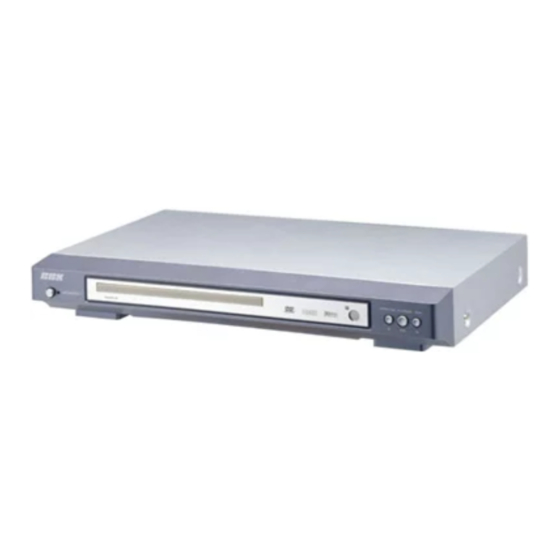
Page 4: Control Button Locations And Explanations
3.Control Button Locations and Explanations Front Panel Illustration POWER switch OPEN/CLOSE button Disc tray PLAY/ PAUSE button IR SENSOR button STOP button... -
Page 5: Prevertion Of Static Electricity Discharge
4.PREVENTION OF STATIC ELECTRICITY DISCHARGE The laser diode in the traverse unit (optical pickup)may brake down due to static electricity of clothes or human body. Use due caution to electrostatic breakdown when servicing and handling the laser diode. 4.1.Grounding for electrostatic breakdown prevention Some devices such as the DVD player use the optical pickup(laser diode)and the optical pickup will be damaged by static electricity in the working environment.Proceed servicing works under the working environment where grounding works is completed. -
Page 6: Assembling And Disassembling The Mechanism Unit
5. Assembling and disassembling the mechanism unit 5.1 Optical pickup Unit Explosed View and Part List Pic (1) - Page 7 Materials to Pic (1) PARTS CODE PARTS NAME Q ty 14692200 SF-HD60 1EA0311A06300 ASSY, CHASSIS, COMPLETE 1EA0M10A15500 ASSY, MOTOR, SLED 1EA0M10A15501 ASSY, MOTOR, SLED 1EA2451A24700 HOLDER, SHAFT 1EA2511A29100 GEAR, RACK 1EA2511A29200 GEAR, DRIVE 1EA2511A29300 GEAR, MIDDLE, A 1EA2511A29400 GEAR, MIDDLE, B 1EA2744A03000 SHAFT, SLIDE 1EA2744A03100...
-
Page 8: Bracket Explosed View And Part List
5.2 Bracket Explosed View and Part List Pic (2) Materials to Pic(2) 1.bracket 14. front silicon rubber 2.belt 15. Back silicon rubber 3.screw 16. Pick-up 4.belt wheel 17. Pick-up 5.gearwheel 18. switch 6.iron chip 19. Five-pin flat plug 7. Immobility mechanism equipment 20. -
Page 9: Miscellaneous
5.3 MISCELLANEOUS 5.3.1 Protection of the LD(Laser diode) Short the parts of LD circuit pattern by soldering. 5.3.2 Cautions on assembly and adjustment Make sure that the workbenches,jigs,tips,tips of soldering irons and measuring instruments are grounded,and that personnel wear wrist straps for ground. Open the LD short lands quickly with a soldering iron after a circuit is connected. -
Page 10: Electrical Confirmation
6.Electrical Confirmation 6.1. Video Output (Luminance Signal) Confirmation DO this confirmation after replacing a P.C.B. Measurement point Mode Disc Color bar 75% DVDT-S15 Video output terminal PLAY(Title 46):DVDT-S15 PLAY(Title 12):DVDT-S01 DVDT-S01 Measuring equipment,tools Confirmation value 200mV/dir,10 sec/dir 1000mVp-p±30mV Purpose:To maintain video signal output compatibility. 1.Connect the oscilloscope to the video output terminal and terminate at 75 ohms. -
Page 11: Video Output(Chrominance Signal) Confirmation
6.2 Video Output(Chrominance Signal) Confirmation Do the confirmation after replacing P.C.B. Measurement point Mode Disc Color bar 75% DVDT-S15 Video output terminal PLAY(Title 46):DVDT-S15 PLAY(Title 12):DVDT-S01 DVDT-S01 Measuring equipment,tools Confirmation value Screwdriver,Oscilloscope 200mV/dir,10 sec/dir 621mVp-p±30mV Purpose:To maintain video signal output compatibility. 1.Connect the oscilloscope to the video output terminal and terminate at 75 ohme. -
Page 12: Mpeg Board Check Waveform
7.MPEG BOARD CHECK WAVEFORM 7.1 27MHz WAVEFORM DIAGRAM 7.2 ICVIPER22 PIN.5 WAVEFORM DIAGRAM... -
Page 13: Ic Block Diagram & Description
MT1336 PRELIMINARY, SUBJ ECT TO CHANGE WITHOUT NOTICE MTK CONFIDENTIAL, NO DISCLOSURE 8. IC BLOCK DIAGRAM & DESCRIPTION 8.1 MT1336 GENERAL DESCRIPTION M T 1 3 3 6 i s a h i g h p e r f o r m a n c e C M O S a n a l o g f r o n t -e n d I C f o r b o t h C D _ R O M d r i v e r u p t o 4 8 X S a n d D V D - R O M d r i v e r u p t o 1 6 X S . - Page 14 MT1336 PRELIMINARY, SUBJ ECT TO CHANGE WITHOUT NOTICE MTK CONFIDENTIAL, NO DISCLOSURE DVDA RFOP DVDB ATTENUATOR INPUT MUX RFON DVDC LRFRP DEFECT DVDD HRFRP CRTP DVDRFIN ENVELOP ENVELOP CRTPLP DETECTOR DETECTOR DVDRFIP REFCOS HALLCOS SBAD COSPHI DPFN REFSIN DPFO HALLSIN SINPHI DPDMUTE MDI2...
- Page 15 MT1336 PRELIMINARY, SUBJ ECT TO CHANGE WITHOUT NOTICE MTK CONFIDENTIAL, NO DISCLOSURE WOBSO WVDD AGNDX DVDA AGNDX DVDB AVDDO DVDC RFOP DVDD RFON DVDRFIP AGNDO DVDRFIN AGNDT MT1336 AVDDT V2REFO RFGC VREFO DVD-ROM RFGCU RFGCI CEQP With CEQN AGNDX DVD_RAM AGNDX VDDP Read...
- Page 16 MT1336 PRELIMINARY, SUBJ ECT TO CHANGE WITHOUT NOTICE MTK CONFIDENTIAL, NO DISCLOSURE MT1336 PIN DESCRIPTIONS Pin Numbers Symbol Type Description LQFP128 RF Flag Interface DEFECT Digital Output Flag of bad data output status RF SIO interface SCLK Digital Input RF serial clock input SDEN Digital Input RF serial data enable...
- Page 17 MT1336 PRELIMINARY, SUBJ ECT TO CHANGE WITHOUT NOTICE MTK CONFIDENTIAL, NO DISCLOSURE RFGCU Analog RF AGC loop capacitor connecting for DVD -RAM RFGCI Analog RF AGC loop capacitor connecting for DVD -RAM Analog Input DC coupled DVD-RAM main-beam RF signal input A Analog Input DC coupled DVD-RAM main-beam RF signal input B Analog Input...
- Page 18 MT1336 PRELIMINARY, SUBJ ECT TO CHANGE WITHOUT NOTICE MTK CONFIDENTIAL, NO DISCLOSURE Analog Input MDI1 Laser power monitor input LDO1 Analog Ou tput Laser driver output Analog Input MDI2 Laser power monitor input LDO2 Analog Output Laser driver output RF RIPPLE CRTP Analog RF top envelop filter capacitor connecting...
- Page 19 MT1336 PRELIMINARY, SUBJ ECT TO CHANGE WITHOUT NOTICE MTK CONFIDENTIAL, NO DISCLOSURE ALPC TRIMMING Analog input Trimming pin for ALPC1 Analog input Trimming pin for ALPC1 Analog input Trimming pin for ALPC2 Analog input Trimming pin for ALPC2 HIGH SPEED TRACK COUNTING TRLP Analog Low-pass filter capacitor connecting...
- Page 20 MT1336 PRELIMINARY, SUBJ ECT TO CHANGE WITHOUT NOTICE MTK CONFIDENTIAL, NO DISCLOSURE...
-
Page 21: Mt1379
MT1379 Progressive Scan DVD Player Combo Chip Speci f i c ati o ns are subj e ct to change wi t hout noti c e 8.2 MT1379 § Tray control can be PWM output or digital output Super Integration DVD player single chip §... - Page 22 MT1379 PRELIMINARY, SUBJECT TO CHANGE WITHOUT NOTICE MTK CONFIDENTIAL, NO DISCLOSURE § cycle timings Downmix function § § Block-based sector addressing Support IEC 60958/61937 output § Programmable buffering counter for buffer status - PCM / bit stream / mute mode tracking - Custom IEC latency up to 2 frames §...
- Page 23 MT1379 PRELIMINARY, SUBJECT TO CHANGE WITHOUT NOTICE MTK CONFIDENTIAL, NO DISCLOSURE EFINITIONS Pin Number Symbol Type Description IREF Analog Input Current reference input. It generates reference current for data PLL. Connect an ext ernal 100K resistor to this pin and PLLVSS. PLLVSS Ground Ground pin for data PLL and related analog circuitry...
- Page 24 MT1379 PRELIMINARY, SUBJECT TO CHANGE WITHOUT NOTICE MTK CONFIDENTIAL, NO DISCLOSURE Pin Number Symbol Type Description HIGHA6 Inout Microcontroller address 14 2~16MA, SR HIGHA7 Inout Microcontroller address 15 2~16MA, SR Inout Microcontroller address/data 7 2~16MA, SR Inout Microcontroller address/data 6 2~16MA, SR Inout Microcontroller address/data 5...
- Page 25 MT1379 PRELIMINARY, SUBJECT TO CHANGE WITHOUT NOTICE MTK CONFIDENTIAL, NO DISCLOSURE Pin Number Symbol Type Description IOA7 Inout Microcontroller address 7 / IO 2~16MA, SR Output Flash address 16 2~16MA, SR Output Flash address 17 2~16MA, SR IOA18 Inout Flash address 18 / IO 2~16MA, SR IOA19 Inout...
- Page 26 MT1379 PRELIMINARY, SUBJECT TO CHANGE WITHOUT NOTICE MTK CONFIDENTIAL, NO DISCLOSURE Pin Number Symbol Type Description UP1_7 Inout Microcontroller port 1 -7 4MA, SR PU, SMT UP3_0 Inout Microcontroller port 3 -0 4MA, SR PU, SMT UP3_1 Inout Microcontroller port 3 -1 4MA, SR PU, SMT INT0#...
- Page 27 MT1379 PRELIMINARY, SUBJECT TO CHANGE WITHOUT NOTICE MTK CONFIDENTIAL, NO DISCLOSURE Pin Number Symbol Type Description RD14 Inout DRAM data 14 2~16MA, SR PU/PD, SMT RD13 Inout DRAM data 13 2~16MA, SR PU/PD, SMT RD12 Inout DRAM data 12 2~16MA, SR PU/PD, SMT DVDD3 Power...
- Page 28 MT1379 PRELIMINARY, SUBJECT TO CHANGE WITHOUT NOTICE MTK CONFIDENTIAL, NO DISCLOSURE Pin Number Symbol Type Description DQM0 Output Mask for DRAM input/output byte 0 2~16MA, SR Output DRAM bank address 0 2~16MA, SR RA10 Output DRAM address10 2~16MA, SR DVDD2 Power 2.5V power pin for internal digital circuitry Output...
- Page 29 MT1379 PRELIMINARY, SUBJECT TO CHANGE WITHOUT NOTICE MTK CONFIDENTIAL, NO DISCLOSURE Pin Number Symbol Type Description RD23 Inout DRAM data 23 / 2~16MA, SR Videoin Data PortA 7 PU/PD, SMT RD22 Inout DRAM data 22 / 2~16MA, SR Videoin Data PortA 6 PU/PD, SMT DVDD2 Power...
- Page 30 MT1379 PRELIMINARY, SUBJECT TO CHANGE WITHOUT NOTICE MTK CONFIDENTIAL, NO DISCLOSURE Pin Number Symbol Type Description ASDATA3 Inout Audio serial data 3 (surround left/surround right channel) Trap value in power-on reset : PD SMT 1 : manufactory test mode 0 : normal operation OR Videoin Data PortB 1 ASDATA4 Inout...
- Page 31 MT1379 PRELIMINARY, SUBJECT TO CHANGE WITHOUT NOTICE MTK CONFIDENTIAL, NO DISCLOSURE Pin Number Symbol Type Description SPDATA Input Audio data of SPDIF input / Videoin Data PortB 5 DVDD2 Power 2.5V power pin for internal digital circuitry SPLRCK Input Audio left/right channel clock of SPDIF input / Videoin Data PortB 6 SPBCK Input...
- Page 32 MT1379 PRELIMINARY, SUBJECT TO CHANGE WITHOUT NOTICE MTK CONFIDENTIAL, NO DISCLOSURE 26 Jul, 2002 Page 1 of 2 IREF YUV0/CIN PLLVSS LPIOP VREF LPION DACVDDC LPFON ASDATA4 LPFIP ASDATA3 LPFIN ASDATA2 LPFOP ASDATA1 JITFO ASDATA0 JITFN SPDIF PLLVDD3 MC_DATA ACLK DVDD3 TROPENPWM ALRCK...
- Page 33 MT1379 PRELIMINARY, SUBJECT TO CHANGE WITHOUT NOTICE MTK CONFIDENTIAL, NO DISCLOSURE UNCTIONAL LOCK D V D m o d u l e S e r v o A n a l o g S p i n d l e D e b u g S y s t e m T V e n c o d e r...
- Page 34 MT1379 PRELIMINARY, SUBJECT TO CHANGE WITHOUT NOTICE MTK CONFIDENTIAL, NO DISCLOSURE controller changes the mode and speed of operation according to servo register setting. The PWM generator generates pulse -width-modulated signal to drive disc spindle motor driver. CSS/CPPM The CSS/CPPM module provides functions necessary for decoding discs conforming to CSS/CPPM specification. System Parser The system parser is used to help the system controller to decode DVD/SVCD/VCD bitstream just after the channel decoder performing error correction.
- Page 35 MT1379 PRELIMINARY, SUBJECT TO CHANGE WITHOUT NOTICE MTK CONFIDENTIAL, NO DISCLOSURE This is a hardware sub-picture decoder. It decodes the compressed SPU image bitstream and CHG_COLCON commands according to SPU header information previously decoded by system controller. The SPU module also allows two SPU objects to be displayed at the same time.
- Page 36 MT1379 PRELIMINARY, SUBJECT TO CHANGE WITHOUT NOTICE MTK CONFIDENTIAL, NO DISCLOSURE LECTRICAL HARACTERISTICS Absolute Maximum Rating Symbol Parameters Value Unit VDD3 3.3V Supply voltage -0.3 to 3.6 VDD2 2.5V Supply voltage -0.3 to 3.0 VDDA Analog Supply voltage -0.3 to 3.6 Input Voltage -0.3 to 5.5 Output Voltage...
-
Page 37: U214 Hy29F800
8.3 U214 HY29F800 KEY FEATURES n Sector Protection n 5 Volt Read, Program, and Erase – Minimizes system-level power requirements – Any combination of sectors may be n High Performance locked to prevent program or erase – Access times as fast as 55 ns operations within those sectors n Low Power Consumption n Temporary Sector Unprotect... - Page 38 BLOCK DIAGRAM DQ[15:0] A[18:0], A-1 STATE C O N T R O L ERASE VOLTAGE I/O BUFFERS G E N E R A T O R A N D DQ[15:0] S E C T O R S W I T C H E S C O M M A N D W E # REGISTER...
- Page 39 PIN CONFIGURATIONS RY/BY# RESET# W E # BYTE# DQ15/A-1 DQ14 DQ13 DQ12 W E # Standard BYTE# RESET# DQ11 TSOP48 DQ15/A-1 RY/BY# DQ10 DQ14 DQ13 DQ10 DQ12 DQ11 BYTE# DQ15/A-1 DQ14 DQ13 DQ12 W E # Reverse RESET# DQ11 TSOP48 RY/BY# DQ10...
-
Page 40: U203 Sdram-Hy57V1610D
8.4 U203 SDRAM-HY57V1610D D E S C R I P T I O N T H E H y n i x H Y 5 7 V 1 6 1 6 1 0 D i s a 1 6 , 7 7 7 , 2 1 6 - b i t s C M O S S y n c h r o n o u s D R A M , i d e a l l y s u i t e d f o r t h e M o b i l e a p p l i c a t i o n s w h i c h r e q u i r e l o w p o w e r c o n s u m p t i o n a n d i n d u s t r i a l t e m p e r a t u r e r a n g e . - Page 41 P I N C O N F I G U R A T I O N V D D V S S D Q 0 D Q 1 5 D Q 1 D Q 1 4 V S S Q V S S Q D Q 2 D Q 1 3...
-
Page 42: Schematic & Pcb Wiring Diagram
9. SCHEMATIC & PCB WIRING DIAGRAM FRONT SCHEMATIC DIAGRAM... - Page 43 FRONT SCHEMATIC DIAGRAM...
- Page 44 POWER BOARD SCHEMATIC DIAGRAM...
- Page 45 POWER BOARD SCHEMATIC DIAGRAM...
- Page 46 MIAN SCHEMATIC DIAGRAM AVDDP AGNDX AGNDP PWMOUT2 DPDMUTE URST AGND SDATA SDATA SDEN AVDD SDEN GNDS SCLK SCLK CDFOP XCK16M CDFON VDDS TRCLOSE SVDD ENDM STBY SGND LIMIT WGAND TROUT AGC1 TRIN WAVDD AGC2 AGC3 MD12 MD11 MD11 LDO1 LDO1 LDO2 LDO2 HDGATE...
- Page 47 MIAN SCHEMATIC DIAGRAM R240 XTALI APLLVDD3 RFIP RFIN R2107 DRD# PRD# IOOE# RFDTSLVN R2108 DWR# PWR# IOWR# RFDTSLVP R2109 DCE# PCE# IOCS# ADCVDD3 DVSS PWM2VREF UP1_2 PWMVREF VSCK RFZC UP1_3 HRFZC C233 VSDA RFRPC UP1_4 RFRP_AC VSTB RFRP UP1_5 RFRP_DC UP1_6 RFLEVEL DVDD3...
- Page 48 MIAN SCHEMATIC DIAGRAM...
- Page 49 MIAN SCHEMATIC DIAGRAM...
- Page 50 MIAN SCHEMATIC DIAGRAM...
-
Page 51: Spare Parts List
10. SPARE PARTS LIST DV911S-2 MATERIAL LIST 1. POWER BOARD MATERIAL CODE MATERIAL NAME SPECIFICATIONS UNIT QUANTITY LOCATION CARBON FILM 1/4W10K±5% SHAPED 10 R507 RESISTOR 0010101 METAL FILM RESISTOR 1/4W12K±1% SHAPED 10 R509 CARBON FILM 0000461 1/4W9.1K±5% SHAPED 10 R512... - Page 52 1563407 5501A-4 2100003 CONNECTION CORDS Φ0.6 SHAPED 7.5mm JP501,JP503 2100010 CONNECTION CORDS Φ0.6 SHAPED 5mm JP502 2300021 FUSE T1.6AL 250V F501 1940045 SOCKET 2P 8.0mm 2# BCN501,BCN502 1940023 SOCKET 7P 2.0mm CN502 1940027 SOCKET 2P 2.0mm CN501 0881933 VIPER22A DIP8 U501 GROUND CHIP OF 3870115...
- Page 53 R211,R222,R223,R2130,R 0090019 SMD RESISTOR 1/16W 4.7K ±5% 2131,R2134,R2135,R343 0090021 SMD RESISTOR 1/16W 6.8K ±5% R2136,R2148 0090022 SMD RESISTOR 1/16W 8.2K ±5% R201 0090016 SMD RESISTOR 1/16W 1.5K ±5% R338,R342 0090223 SMD RESISTOR 1/16W 2K ±5% R237 0090011 SMD RESISTOR 1/16W 470Ω ±5% R322,R323 R206,R250,R265,R303~R 0090023...
- Page 54 C201~C211,C221,C224,C 227,C230,C231,C232,C23 4,C235,C237,C240,C245~ C253,C279,C282,C289~C 291,C294~C297,C301~C3 03,C312~C313,C320~C33 0310058 SMD CAPACITOR 25V 104 +80%-20% 0603 0,C332,C335~C339,C341, C2113,C2137,C2142,C214 4,C2146,C2150~C2154,C2 157,C2158,C2165,C2159, C2160,C2161~C2164,C28 0310234 SMD CAPACITOR 16V 105 +80%-20% 0603 C315~C318 C233,C238,C239,C2112,C 0310066 SMD CAPACITOR 50V 102 ±10% 0603 2115,C2148,,C299,C2101 0310231 SMD CAPACITOR 50V 122 ±10% 0603 C2122,C2129 0310072 SMD CAPACITOR...
- Page 55 SA-001-012 BLACK IRON SHEET 1910129 TERMINAL SOCKET JK202 SCREEN-SHIELDED 1940024 SOCKET 5P 2.0mm XS302 1940005 SOCKET 6P 2.0mm XS201,XS303 1940023 SOCKET 7P 2.0mm XS203 1631550 2911S-1 1940094 CABLE SOCKET 24P 0.5mm SMD WITH CLASP XS301...
Need help?
Do you have a question about the DV911S and is the answer not in the manual?
Questions and answers