Table of Contents
Advertisement
Quick Links
Advertisement
Table of Contents

Related Manuals for BBK DV964S


Summary of Contents for BBK DV964S
- Page 1 SERVICE MANUAL DV964S POWER...
-
Page 2: Table Of Contents
CONTENTS SAFETY PRECAUTIONS PREVENTION OF ELECTRO STATIC DISCHARGE(ESD)TO ELECTROSTATICALLY SENSITIVE(ES)DEVICES CONTROL BUTTON LOCATIONS AND EXPLANATIONS PREVERTION OF STATIC ELECTRICITY DISCHARGE ASSEMBLING AND DISASSEMBLING THE MECHANISM UNIT OPTICAL PICKUP UNIT EXPLOSED VIEW AND PART LIST BRACKET EXPLOSED VIEW AND PART LIST MISCELLANEOUS ELECTRICAL CONFIRMATION VIDEO OUTPUT (LUMINANCE SIGNAL) CONFIRMATION... -
Page 3: Safety Precautions
1. SAFETY PREAUTIONS 1.1 GENERAL GUIDELINES 1. When servicing, observe the original lead dress. if a short circuit is found, replace all parts which have been overheated or damaged by the short circuit. 2. After servicing, see to it that all the protective devices such as insulation barrier, insulation papers shields are properly installed. -
Page 4: Control Button Locations And Explanations
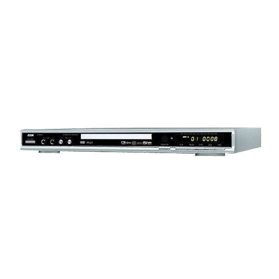
Front Panel Illustration POWER POWER switch MIC 2 jack PAUSE button Disc tray MIC VOLUME 1 knob STOP button IR SENSOR MIC VOLUME 2 knob REW button Display window OPEN/CLOSE button FWD button MIC 1 jack PLAY button... -
Page 5: Prevertion Of Static Electricity Discharge
4.PREVENTION OF STATIC ELECTRICITY DISCHARGE The laser diode in the traverse unit (optical pickup)may brake down due to static electricity of clothes or human body. Use due caution to electrostatic breakdown when servicing and handling the laser diode. 4.1.Grounding for electrostatic breakdown prevention Some devices such as the DVD player use the optical pickup(laser diode)and the optical pickup will be damaged by static electricity in the working environment.Proceed servicing works under the working environment where grounding works is completed. -
Page 6: Assembling And Disassembling The Mechanism Unit
5. Assembling and disassembling the mechanism unit 5.1 Optical pickup Unit Explosed View and Part List Pic (1) - Page 7 Materials to Pic (1) PARTS CODE PARTS NAME Q ty 14692200 SF-HD60 1EA0311A06300 ASSY, CHASSIS, COMPLETE 1EA0M10A15500 ASSY, MOTOR, SLED 1EA0M10A15501 ASSY, MOTOR, SLED 1EA2451A24700 HOLDER, SHAFT 1EA2511A29100 GEAR, RACK 1EA2511A29200 GEAR, DRIVE 1EA2511A29300 GEAR, MIDDLE, A 1EA2511A29400 GEAR, MIDDLE, B 1EA2744A03000 SHAFT, SLIDE 1EA2744A03100...
-
Page 8: Bracket Explosed View And Part List
5.2 Bracket Explosed View and Part List Pic (2) Materials to Pic(2) 1.bracket 14. front silicon rubber 2.belt 15. Back silicon rubber 3.screw 16. Pick-up 4.belt wheel 17. Pick-up 5.gearwheel 18. switch 6.iron chip 19. Five-pin flat plug 7. Immobility mechanism equipment 20. -
Page 9: Miscellaneous
5.3 MISCELLANEOUS 5.3.1 Protection of the LD(Laser diode) Short the parts of LD circuit pattern by soldering. 5.3.2 Cautions on assembly and adjustment Make sure that the workbenches,jigs,tips,tips of soldering irons and measuring instruments are grounded,and that personnel wear wrist straps for ground. Open the LD short lands quickly with a soldering iron after a circuit is connected. -
Page 10: Electrical Confirmation
6.Electrical Confirmation 6.1. Video Output (Luminance Signal) Confirmation DO this confirmation after replacing a P.C.B. Measurement point Mode Disc Color bar 75% DVDT-S15 Video output terminal PLAY(Title 46):DVDT-S15 PLAY(Title 12):DVDT-S01 DVDT-S01 Measuring equipment,tools Confirmation value 200mV/dir,10 sec/dir 1000mVp-p±30mV Purpose:To maintain video signal output compatibility. 1.Connect the oscilloscope to the video output terminal and terminate at 75 ohms. -
Page 11: Video Output(Chrominance Signal) Confirmation
6.2 Video Output(Chrominance Signal) Confirmation Do the confirmation after replacing P.C.B. Measurement point Mode Disc Color bar 75% DVDT-S15 Video output terminal PLAY(Title 46):DVDT-S15 PLAY(Title 12):DVDT-S01 DVDT-S01 Measuring equipment,tools Confirmation value Screwdriver,Oscilloscope 200mV/dir,10 sec/dir 621mVp-p±30mV Purpose:To maintain video signal output compatibility. 1.Connect the oscilloscope to the video output terminal and terminate at 75 ohme. -
Page 12: Mpeg Board Check Waveform
7.MPEG BOARD CHECK WAVEFORM 7.1 27MHz WAVEFORM DIAGRAM 7.2 IC5L0380R PIN.2 WAVEFORM DIAGRAM... -
Page 13: Am29Lv160D
8. Am29LV160D 16 Megabit (2 M x 8-Bit/1 M x 16-Bit) CMOS 3.0 Volt-only Boot Sector Flash Memory DISTINCTIVE CHARACTERISTICS Single power supply operation Embedded Algorithms — Full voltage range: 2.7 to 3.6 volt read and write — Embedded Erase algorithm automatically operations for battery-powered applications preprograms and erases the entire chip or any combination of designated sectors... - Page 14 PRODUCT SELECTOR GUIDE Family Part Number Am29LV160D Speed Option Voltage Range: V = 2.7–3.6 V -120 Max access time, ns (t Max CE# access time, ns (t Max OE# access time, ns (t Note: See “AC Characteristics” for full specifications. BLOCK DIAGRAM –...
- Page 15 CONNECTION DIAGRAMS BYTE# DQ15/A-1 DQ14 DQ13 DQ12 Standard TSOP RESET# DQ11 RY/BY# DQ10 BYTE# DQ15/A-1 DQ14 DQ13 DQ12 RESET# Reverse TSOP DQ11 RY/BY# DQ10...
- Page 16 CONNECTION DIAGRAMS RESET# BYTE# DQ15/A-1 DQ14 DQ13 DQ10 DQ12 DQ11 FBGA Top View, Balls Facing Down BYTE# DQ15/A-1 DQ14 DQ13 RESET# DQ12 RY/BY# DQ10 DQ11 Special Handling Instructions Flash memory devices in FBGA packages may be damaged if exposed to ultrasonic cleaning methods. Special handling is required for Flash Memory products The package and/or data integrity may be compromised in FBGA packages.
- Page 17 PIN CONFIGURATION LOGIC SYMBOL A0–A19 = 20 addresses DQ0–DQ14 = 15 data inputs/outputs A0–A19 16 or 8 DQ15/A-1 = DQ15 (data input/output, word mode), DQ0–DQ15 A-1 (LSB address input, byte mode) (A-1) BYTE# = Selects 8-bit or 16-bit mode = Chip enable = Output enable = Write enable RESET#...
-
Page 18: Hy57V641620Hg
HY57V641620HG 4 Banks x 1M x 16Bit Synchronous DRAM 8.1 HY57V641620HG DESCRIPTION The Hyundai HY57V641620HG is a 67,108,864-bit CMOS Synchronous DRAM, ideally suited for the main memory applications which require large memory density and high bandwidth. HY57V641620HG is organized as 4banks of 1,048,576x16. HY57V641620HG is offering fully synchronous operation referenced to a positive edge of the clock. - Page 19 HY57V641620HG PIN CONFIGURATION DQ15 DQ14 DQ13 DQ12 DQ11 DQ10 54pin TSOP II 400mil x 875mil 0.8mm pin pitch LDQM UDQM /CAS /RAS A10/AP PIN DESCRIPTION PIN NAME DESCRIPTION The system clock input. All other inputs are registered to the SDRAM on the Clock rising edge of CLK Controls internal clock signal and when deactivated, the SDRAM will be one...
- Page 20 HY57V641620HG FUNCTIONAL BLOCK DIAGRAM 1Mbit x 4banks x 16 I/O Synchronous DRAM Self refresh logic Internal Row & timer counter 1Mx16 Bank 3 1Mx16 Bank 2 Row active Decoders 1Mx16 Bank 1 1Mx16 Bank 0 Memory refresh Cell Array Column Column Active UDQM...
-
Page 21: Mt1389
8.2 MT1389 MT1389 Progressive-Scan DVD Player SOC Specifications are subject to change without notice MediaTek MT1389 is a DVD player system-on-chip (SOC) which incorporates advanced features like high quality TV encoder and state-of-art de-interlace processing. The MT1389 enables consumer electronics manufacturers to build high quality, cost-effective DVD players, portable DVD players or any other home entertainment audio/video devices. - Page 22 MT1389 PRELIMINARY, SUBJECT TO CHANGE WITHOUT NOTICE MTK CONFIDENTIAL, NO DISCLOSURE General Feature List 1024-bytes on-chip RAM Super Integration DVD player single chip Up to 4M bytes FLASH-programming interface High performance analog RF amplifier Supports 5/3.3-Volt. FLASH interface Servo controller and data channel processing Supports power-down mode MPEG-1/MPEG-2/JPEG video Supports additional serial port...
- Page 23 MT1389 PRELIMINARY, SUBJECT TO CHANGE WITHOUT NOTICE MTK CONFIDENTIAL, NO DISCLOSURE Audio Effect Processing TV Encoder Dolby Digital (AC-3)/EX decoding Six 108MHz/12bit DACs DTS/DTS-ES decoding Support NTSC, PAL-BDGHINM, PAL-60 MLP decoding for DVD-Audio Support 525p, 625p progressive TV format MPEG-1 layer 1/layer 2 audio decoding Automatically turn off unconnected channels MPEG-2 layer1/layer2 2-channel audio Support PC monitor (VGA)
-
Page 24: Schematic & Pcb Wiring Diagram
9. SCHEMATIC & PCB WIRING DIAGRAM FRONT SCHEMATIC DIAGRAM... - Page 25 FRONT SCHEMATIC DIAGRAM...
- Page 26 POWER BOARD SCHEMATIC DIAGRAM...
- Page 27 POWER BOARD SCHEMATIC DIAGRAM...
- Page 28 OK SCHEMATIC DIAGRAM...
- Page 29 OK SCHEMATIC DIAGRAM...
- Page 30 OUTPUT BOARD SCHEMATIC DIAGRAM...
- Page 31 OUTPUT BOARD SCHEMATIC DIAGRAM...
- Page 32 MIAN SCHEMATIC DIAGRAM...
- Page 33 MIAN SCHEMATIC DIAGRAM...
- Page 34 MIAN SCHEMATIC DIAGRAM...
- Page 35 MIAN SCHEMATIC DIAGRAM...
-
Page 36: Spare Parts List
10. SPARE PARTS LIST DV964s MATERIAL LIST 1. DECODE BOARD MATERIAL SPECIFICATIONS/PART NUMBER QUANTITY LOCATION C2119,C2128,C2131,L210~L2 15,R201~R204,R212,R221,R2 26,R228,R234,R236,R245,R2 SMD RESISTOR 1/16W 0Ω ±5% 47,R222,R251,R255,R257,R2 58,R282,R297,R298,R299,R3 03,R318,R331,R2159,R268,R R233,R261,R270,R273,R274,R27 SMD RESISTOR 1/16W 75Ω ±5% 6,R280 CARBON FILM RESISTOR 1/4W2.2Ω±5% R326 SMD RESISTOR 1/16W1Ω±5%... - Page 37 C262~C266,C289,C290,C292, SMD CAPACITOR 50V 47P ±5% NPO 0603 C293,C295,C296,C298,C299, C2101,C2102,C2104,C2105 C233,C2111,C2114,C2117,C2120 SMD CAPACITOR 50V 101 ±5% NPO 0603 ,C2123,C2126,C206 SMD CAPACITOR 50V 331 ±5% NPO 0603 C212,C213 SMD CAPACITOR 50V 151 ±5% NPO 0603 C304,C306 C207,C211,C214,C216,C217, C224,C226~C231,C234~C239 ,C241~C254,C256~C259,C26 7~C274,C279,C2170~C2171, SMD CAPACITOR 50V 104 +80%-20% 0603 C301~C303,C305,C309,C311, C312,C2138~C2143,C2153~C...
- Page 38 SMD TRIODE C1815 Q205~Q210 TRIODE 2SA1015 Q211,Q218,Q219 SMD TRIODE 3904 V305 SMD TRIODE 2SK3018 V303,V304 SMD TRIODE 2SB1132 V301,V302 NJM4558M SOP U219,U220,U221 64.1 IC RC4558D SOP U219,U220,U221 MM74HCU04M SOP U205 65.1 IC HCU04 SOP U205 HY57V641620HGT-7 TSOP U211 66.1 IC KSV464P4JA-70 TSOP U211 LM1117MP-ADJ SOT-223...
- Page 39 CD11T 10V1000u±20%8×16 3.5 TC505,TC506,TC509,TC510 CD288H 400V47U±20%22×25 10 TC501 MAGNETIC BEADS INDUCTORH354708 L503 CHOKE COIL VERTICAL 10UH 1A 5mm L505 CHOKE COIL VERTICAL 10UH 2A 5mm L506,L507 SWITCHING POWER BCK-28-0286 T501 TRANSFORMER SWITCHING POWER 26.1 BCK2801-624 T501 TRANSFORMER DIODE HER105 D506,D508,D511 DIODE HER306 D510...
- Page 40 CARBON FILM RESISTOR 1/6W100K±5% SHAPED 7.5 R615,R617 CARBON FILM RESISTOR 1/6W4.7K±5% SHAPED 7.5 R611,R612 ROTATED POTENTIOMETERWH09NTX-1C-A10K-F30 VR601,VR602 PORCELAIN CAPACITOR 50V 47P ±5% NPO 5mm C605,C606 12.1 PORCELAIN CAPACITOR 50V 47P ±5% 5mm C605,C606 12.2 PORCELAIN CAPACITOR 50V 47P ±10% 5mm C605,C606 PORCELAIN CAPACITOR 50V 100P ±10% 5mm...
- Page 41 ELECTRO-OPTIC 19.1 TX179AT JK705 TRANSFORMER TERMINAL SOCKET AV4-8.4-6G-5 JK702 TERMINAL SOCKET AV8-8.4-6G-3 JK701 SCART SOCKET SCART-01 JK706 7939B-0 CABLE SOCKET 14P 1.0mm STRAIGHT DUAL LINE PLU XS701 TERMINAL SOCKET AV1-8.4-5G-2 BLACK JK704 TERMINAL SOCKET S-VIDEO JK703 CONNECTION CORDS Φ0.6 SHAPED 5mm JP701~JP703,JP705--JP708 CONNECTION CORDS Φ0.6 SHAPED 10mm...
Need help?
Do you have a question about the DV964S and is the answer not in the manual?
Questions and answers