Table of Contents
Advertisement
Quick Links
Advertisement
Table of Contents

Subscribe to Our Youtube Channel
Related Manuals for BBK DV722S


Summary of Contents for BBK DV722S
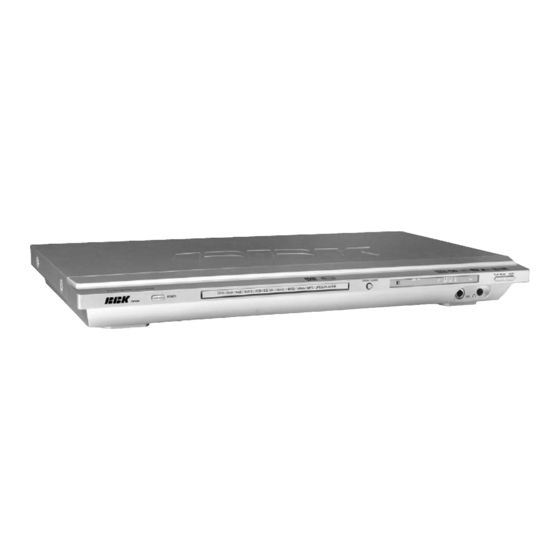
- Page 1 SERVICE MANUAL DV722S...
-
Page 2: Table Of Contents
CONTENTS SAFETY PRECAUTIONS PREVENTION OF ELECTRO STATIC DISCHARGE(ESD)TO ELECTROSTATICALLY SENSITIVE(ES)DEVICES CONTROL BUTTON LOCATIONS AND EXPLANATIONS PREVERTION OF STATIC ELECTRICITY DISCHARGE ASSEMBLING AND DISASSEMBLING THE MECHANISM UNIT OPTICAL PICKUP UNIT EXPLOSED VIEW AND PART LIST BRACKET EXPLOSED VIEW AND PART LIST MISCELLANEOUS ELECTRICAL CONFIRMATION VIDEO OUTPUT (LUMINANCE SIGNAL) CONFIRMATION... -
Page 3: Safety Precautions
1. SAFETY PREAUTIONS 1.1 GENERAL GUIDELINES 1. When servicing, observe the original lead dress. if a short circuit is found, replace all parts which have been overheated or damaged by the short circuit. 2. After servicing, see to it that all the protective devices such as insulation barrier, insulation papers shields are properly installed. -
Page 5: Prevention Of Static Electricity Discharge
4.PREVENTION OF STATIC ELECTRICITY DISCHARGE The laser diode in the traverse unit (optical pickup)may brake down due to static electricity of clothes or human body. Use due caution to electrostatic breakdown when servicing and handling the laser diode. 4.1.Grounding for electrostatic breakdown prevention Some devices such as the DVD player use the optical pickup(laser diode)and the optical pickup will be damaged by static electricity in the working environment.Proceed servicing works under the working environment where grounding works is completed. -
Page 6: Assembling And Disassembling The Mechanism Unit
5. Assembling and disassembling the mechanism unit 5.1 Optical pickup Unit Explosed View and Part List Pic (1) - Page 7 Materials to Pic (1) PARTS CODE PARTS NAME Q ty 14692200 SF-HD60 1EA0311A06300 ASSY, CHASSIS, COMPLETE 1EA0M10A15500 ASSY, MOTOR, SLED 1EA0M10A15501 ASSY, MOTOR, SLED 1EA2451A24700 HOLDER, SHAFT 1EA2511A29100 GEAR, RACK 1EA2511A29200 GEAR, DRIVE 1EA2511A29300 GEAR, MIDDLE, A 1EA2511A29400 GEAR, MIDDLE, B 1EA2744A03000 SHAFT, SLIDE 1EA2744A03100...
-
Page 8: Bracket Explosed View And Part List
5.2 Bracket Explosed View and Part List Pic (2) Materials to Pic(2) 1.bracket 14. front silicon rubber 2.belt 15. Back silicon rubber 3.screw 16. Pick-up 4.belt wheel 17. Pick-up 5.gearwheel 18. switch 6.iron chip 19. Five-pin flat plug 7. Immobility mechanism equipment 20. -
Page 9: Miscellaneous
5.3 MISCELLANEOUS 5.3.1 Protection of the LD(Laser diode) Short the parts of LD circuit pattern by soldering. 5.3.2 Cautions on assembly and adjustment Make sure that the workbenches,jigs,tips,tips of soldering irons and measuring instruments are grounded,and that personnel wear wrist straps for ground. Open the LD short lands quickly with a soldering iron after a circuit is connected. -
Page 10: Electrical Confirmation
6.Electrical Confirmation 6.1. Video Output (Luminance Signal) Confirmation DO this confirmation after replacing a P.C.B. Measurement point Mode Disc Color bar 75% DVDT-S15 Video output terminal PLAY(Title 46):DVDT-S15 PLAY(Title 12):DVDT-S01 DVDT-S01 Measuring equipment,tools Confirmation value 200mV/dir,10 sec/dir 1000mVp-p±30mV Purpose:To maintain video signal output compatibility. 1.Connect the oscilloscope to the video output terminal and terminate at 75 ohms. -
Page 11: Video Output(Chrominance Signal) Confirmation
6.2 Video Output(Chrominance Signal) Confirmation Do the confirmation after replacing P.C.B. Measurement point Mode Disc Color bar 75% DVDT-S15 Video output terminal PLAY(Title 46):DVDT-S15 PLAY(Title 12):DVDT-S01 DVDT-S01 Measuring equipment,tools Confirmation value Screwdriver,Oscilloscope 200mV/dir,10 sec/dir 621mVp-p±30mV Purpose:To maintain video signal output compatibility. 1.Connect the oscilloscope to the video output terminal and terminate at 75 ohme. -
Page 12: Mpeg Board Check Waveform
7.MPEG BOARD CHECK WAVEFORM 7.1 27MHz WAVEFORM DIAGRAM 7.2 IC5L0380R PIN.2 WAVEFORM DIAGRAM... -
Page 13: Am29Lv160D
8. Am29LV160D 16 Megabit (2 M x 8-Bit/1 M x 16-Bit) CMOS 3.0 Volt-only Boot Sector Flash Memory DISTINCTIVE CHARACTERISTICS Single power supply operation Embedded Algorithms — Full voltage range: 2.7 to 3.6 volt read and write — Embedded Erase algorithm automatically operations for battery-powered applications preprograms and erases the entire chip or any combination of designated sectors... -
Page 14: Block Diagram
PRODUCT SELECTOR GUIDE Family Part Number Am29LV160D Speed Option Voltage Range: V = 2.7–3.6 V -120 Max access time, ns (t Max CE# access time, ns (t Max OE# access time, ns (t Note: See “AC Characteristics” for full specifications. BLOCK DIAGRAM –... - Page 15 CONNECTION DIAGRAMS BYTE# DQ15/A-1 DQ14 DQ13 DQ12 Standard TSOP RESET# DQ11 RY/BY# DQ10 BYTE# DQ15/A-1 DQ14 DQ13 DQ12 RESET# Reverse TSOP DQ11 RY/BY# DQ10...
- Page 16 CONNECTION DIAGRAMS RESET# BYTE# DQ15/A-1 DQ14 DQ13 DQ10 DQ12 DQ11 FBGA Top View, Balls Facing Down BYTE# DQ15/A-1 DQ14 DQ13 RESET# DQ12 RY/BY# DQ10 DQ11 Special Handling Instructions Flash memory devices in FBGA packages may be damaged if exposed to ultrasonic cleaning methods. Special handling is required for Flash Memory products The package and/or data integrity may be compromised in FBGA packages.
- Page 17 PIN CONFIGURATION LOGIC SYMBOL A0–A19 = 20 addresses DQ0–DQ14 = 15 data inputs/outputs A0–A19 16 or 8 DQ15/A-1 = DQ15 (data input/output, word mode), DQ0–DQ15 A-1 (LSB address input, byte mode) (A-1) BYTE# = Selects 8-bit or 16-bit mode = Chip enable = Output enable = Write enable RESET#...
-
Page 18: Hy57V641620Hg
HY57V641620HG 4 Banks x 1M x 16Bit Synchronous DRAM 8.1 HY57V641620HG DESCRIPTION The Hyundai HY57V641620HG is a 67,108,864-bit CMOS Synchronous DRAM, ideally suited for the main memory applications which require large memory density and high bandwidth. HY57V641620HG is organized as 4banks of 1,048,576x16. HY57V641620HG is offering fully synchronous operation referenced to a positive edge of the clock. - Page 19 HY57V641620HG PIN CONFIGURATION DQ15 DQ14 DQ13 DQ12 DQ11 DQ10 54pin TSOP II 400mil x 875mil 0.8mm pin pitch LDQM UDQM /CAS /RAS A10/AP PIN DESCRIPTION PIN NAME DESCRIPTION The system clock input. All other inputs are registered to the SDRAM on the Clock rising edge of CLK Controls internal clock signal and when deactivated, the SDRAM will be one...
-
Page 20: Functional Block Diagram
HY57V641620HG FUNCTIONAL BLOCK DIAGRAM 1Mbit x 4banks x 16 I/O Synchronous DRAM Self refresh logic Internal Row & timer counter 1Mx16 Bank 3 1Mx16 Bank 2 Row active Decoders 1Mx16 Bank 1 1Mx16 Bank 0 Memory refresh Cell Array Column Column Active UDQM... -
Page 21: Mt1389
8.2 MT1389 MT1389 Progressive-Scan DVD Player SOC Specifications are subject to change without notice MediaTek MT1389 is a DVD player system-on-chip (SOC) which incorporates advanced features like high quality TV encoder and state-of-art de-interlace processing. The MT1389 enables consumer electronics manufacturers to build high quality, cost-effective DVD players, portable DVD players or any other home entertainment audio/video devices. - Page 22 MT1389 PRELIMINARY, SUBJECT TO CHANGE WITHOUT NOTICE MTK CONFIDENTIAL, NO DISCLOSURE General Feature List 1024-bytes on-chip RAM Super Integration DVD player single chip Up to 4M bytes FLASH-programming interface High performance analog RF amplifier Supports 5/3.3-Volt. FLASH interface Servo controller and data channel processing Supports power-down mode MPEG-1/MPEG-2/JPEG video Supports additional serial port...
- Page 23 MT1389 PRELIMINARY, SUBJECT TO CHANGE WITHOUT NOTICE MTK CONFIDENTIAL, NO DISCLOSURE Audio Effect Processing TV Encoder Dolby Digital (AC-3)/EX decoding Six 108MHz/12bit DACs DTS/DTS-ES decoding Support NTSC, PAL-BDGHINM, PAL-60 MLP decoding for DVD-Audio Support 525p, 625p progressive TV format MPEG-1 layer 1/layer 2 audio decoding Automatically turn off unconnected channels MPEG-2 layer1/layer2 2-channel audio Support PC monitor (VGA)
-
Page 24: Cd4052B
CD4051B, CD4052B, CD4053B 8.3 CD4052B Data sheet acquired from Harris Semiconductor August 1998 - Revised March 2000 SCHS047D CMOS Analog Multiplexers/Demultiplexers Features with Logic Level Conversion • Wide Range of Digital and Analog Signal Levels - Digital ......3V to 20V The CD4051B, CD4052B, and CD4053B analog multiplexers - Analog. - Page 25 CD4051B, CD4052B, CD4053B Pinouts CD4051B (PDIP, CDIP, SOIC, TSSOP) CD4052B (PDIP, CDIP, TSSOP) TOP VIEW TOP VIEW Y CHANNELS CHANNELS IN/OUT IN/OUT X CHANNELS IN/OUT COM OUT/IN COMMON “Y” OUT/IN CHANNELS IN/OUT COMMON “X” OUT/IN Y CHANNELS CHANNELS IN/OUT IN/OUT X CHANNELS IN/OUT CD4053B (PDIP, CDIP, TSSOP)
- Page 26 CD4051B, CD4052B, CD4053B Functional Block Diagrams (Continued) CD4052B X CHANNELS IN/OUT COMMON X OUT/IN † BINARY LOGIC 1 OF 4 † COMMON Y LEVEL DECODER OUT/IN CONVERSION WITH † INHIBIT Y CHANNELS IN/OUT CD4053B BINARY TO 1 OF 2 IN/OUT LOGIC DECODERS 16 V...
- Page 27 CD4051B, CD4052B, CD4053B TRUTH TABLES INPUT STATES INHIBIT “ON” CHANNEL(S) CD4051B None CD4052B INHIBIT 0x, 0y 1x, 1y 2x, 2y 3x, 3y None CD4053B INHIBIT A OR B OR C ax or bx or cx ay or by or cy None X = Don’t Care...
-
Page 28: Schematic & Pcb Wiring Diagram
9. SCHEMATIC & PCB WIRING DIAGRAM FRONT SCHEMATIC DIAGRAM... - Page 29 FRONT SCHEMATIC DIAGRAM...
- Page 30 POWER BOARD SCHEMATIC DIAGRAM...
- Page 31 POWER BOARD SCHEMATIC DIAGRAM...
- Page 32 OK SCHEMATIC DIAGRAM...
- Page 33 OK SCHEMATIC DIAGRAM...
- Page 34 OUTPUT BOARD SCHEMATIC DIAGRAM...
- Page 35 OUTPUT BOARD SCHEMATIC DIAGRAM...
- Page 36 MIAN SCHEMATIC DIAGRAM...
- Page 37 MIAN SCHEMATIC DIAGRAM...
- Page 38 MIAN SCHEMATIC DIAGRAM...
- Page 39 MIAN SCHEMATIC DIAGRAM...
- Page 40 MIAN SCHEMATIC DIAGRAM...
-
Page 41: Spare Parts List
10. SPARE PARTS LIST DV722S MATERIAL LIST 1. POWER BOARD MATERIAL CODE MATERIAL NAME SPECIFICATIONS UNIT UANTIT LOCATION 0000273 CARBON FILM RESISTOR 1/4W33Ω±5% SHAPED 10 R505 0000278 CARBON FILM RESISTOR 1/4W330Ω±5% SHAPED 10 R506 0000294 CARBON FILM RESISTOR 1/4W10K±5% SHAPED 10... - Page 42 2100006 CONNECTION CORDS Φ0.6 SHAPED 12.5mm JP504,JP505 2300021 FUSE T1.6AL 250V WITH PIN F501 U501,U504 FOR HEAT 3580039 HEAT RADIATION BOARD 11×15×25 AB009K RADIATION U501,U504 FOR HEAT 3580054 HEAT RADIATION BOARD 11×15×25 WHITE AB905 RADIATION 1563276 59904S-1 GROUND CHIP OF POWER 3870115 AB903 G501,G502...
- Page 43 15P 1.0mm DUAL LINE TOUCH POINT 1940193 CABLE SOCKET XS701 STRAIGHT PLUG JP701,JP704,JP711~JP712,J 2100010 CONNECTION CORDS Φ0.6 SHAPED 5mm P721~JP727 2100003 CONNECTION CORDS Φ0.6 SHAPED 7.5mm JP703,JP713~JP718,JP720 2100004 CONNECTION CORDS Φ0.6 SHAPED 10mm JP705,JP709,JP719 2100006 CONNECTION CORDS Φ0.6 SHAPED 12.5mm JP702 1860029 SCART SOCKET...
- Page 44 0000375 CARBON FILM RESISTOR 1/4W2.2Ω±5% R326 0090272 SMD RESISTOR 1/16W1Ω±5% 0603 R304~R307,R321,R340 0090003 SMD RESISTOR 1/16W 10Ω ±5% 0603 R301,R302 R231,R232,R256,R263~R267, 0090005 SMD RESISTOR 1/16W 33Ω ±5% 0603 R291~R296,R2162 ,L202 0090232 SMD RESISTOR 1/16W 150Ω ±5% 0603 R2180 0090008 SMD RESISTOR 1/16W 220Ω...
- Page 45 C207,C211,C214,C216,C217, C224,C226~C231,C234~C239 ,C241~C254,C256~C259,C26 7~C274,C279,C301~C303,C3 05,C309,C311,C312,C2138~C 0310084 SMD CAPACITOR 50V 104 +80%-20% 0603 2140,C2153~C2157,C2161,C2 163,C2169,C2166,C2174,C21 75,C2168,C2100,C2179,C218 1,C356,C357,C2164,C2171,C 2167,C2176,C2177,C2178,C2 150~C2152,C287,C284 C207,C211,C214,C216,C217, C224,C226~C231,C234~C239 ,C241~C254,C256~C259,C26 7~C274,C279,C301~C303,C3 05,C309,C311,C312,C2138~C 0310058 SMD CAPACITOR 25V 104 +80%-20% 0603 2140,C2153~C2157,C2161,C2 163,C2169,C2166,C2174,C21 75,C2168,C2100,C2179,C218 1,C356,C357,C2164,C2171,C 2167,C2176,C2177,C2178,C2 150~C2152,C287,C284 C201~C204,C221,C240,C285, 0310234 SMD CAPACITOR 16V 105 +80%-20% 0603 C286 C2112,C2115,C2118,C2121,C...
- Page 46 0880513 HCU04 SOP U205 0881415 HY57V641620HGT-7 TSOP U211 0881872 KSV464P4JA-70 TSOP U211 881182 LM1117MP-ADJ SOT-223 U209 0881057 CS4360 SSOP U207 0881059 CS5333 SSOP U210 0881031 24C02N SOP U202 0881897 MT1389EE QFP U201 0881994 MT1389FE QFP U201 0881378 BA5954FP HSOP U302 0881886 36C7T 3MCD4052BM SOP U304...
-
Page 47: Appendix-Am/Fm Tuner Specificadtion
11. APPENDIX-AM/FM Tuner Specificadtion... - Page 70 30 % less volume than our traditional models thanks to state-of-the-art customized IC. Features Uniquely developed IC has achieved a small volume of 60 ml, 30 % less than our traditional models. Fully shielded structure with ANT connector effectively filters out noise. Applications Offers a wide range applications to audio equipment, especially multi-functional, compact...
- Page 71 TFCF Series FM/AM Combination Tuner with Noise Immunizing Structure Dimensions Unit : mm 20max. 12.5 60max. 0.85 AM ANT (9.9) (9.4) Terminal Terminal name FM DET Rch OUT Lch OUT 40.25 (27) Circuit Block Diagram FM/AM/PLL Combination IC...
Need help?
Do you have a question about the DV722S and is the answer not in the manual?
Questions and answers